Modulation of Donor-Acceptor Interface through Thermal Treatment for Efficient Bilayer
Organic Solar Cells
Dhananjaya Kekuda,†Jen-Hsien Huang,‡ Kuo-Chuan Ho,‡and Chih-Wei Chu*,†,§
Research Center for Applied Sciences, Academia Sinica, Taipei, Taiwan 11529, Department of Chemical Engineering, National Taiwan UniVersity, Taipei 10617, Taiwan, and Department of Photonics, National Chiao Tung UniVersity, Hsinchu 30013, Taiwan
ReceiVed: October 20, 2009; ReVised Manuscript ReceiVed: December 23, 2009
In this article, we demonstrate the effect of donor-acceptor (D-A) interface on the performance of bilayer organic solar cells. Solution processing was used to develop liquid crystal poly(9,9 ′-dioctylfluorene-co-bithiophene) (F8T2) polymer films and variable morphology of the films was achieved by varying the annealing temperature. The morphology of the annealed active layers signature a well-aligned nanodomain feature with an interdegitated structure at 200°C. The devices with bilayer configuration, ITO/PEDOT:PSS/F8T2/C70/Al,
have yielded a power conversion efficiency (PCE) of 3.4((0.2)% under 1 sun incident radiation. We attribute the high PCE to the increased D-A junction interface and balanced charge transport between electron/hole transport layers.
Introduction
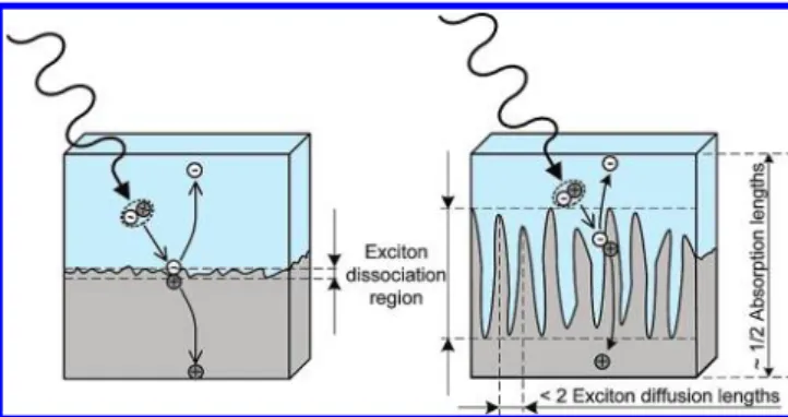
Since the first p-n junction organic solar cell was invented in 1986 by Tang et al,1 it has progressed vastly in recent years.2-5Attempts to construct bilayer solar cells have also been reported recently which were found in different device con-figurations as well as variety of material combinations.6,7 However, their performance was by far not in comparison with that of the bulk heterojunction counterparts. This was mainly due to the following reasons: (i) lower heterojunction interfacial area available for the exciton dissociation, (ii) low mobility and unbalanced charge transport in the bilayer structures, (iii) incompatibility of the interfaces of the organic/inorganic sys-tem,8 and (iv) limitations on the thickness of the individual layers. Hence, if the bilayer structures can take into consideration the aforementioned factors, they can still compete with the bulk heterojunction counterparts. In the case of bilayer solar cells, in order to overcome the issues of lower heterojunction interfacial area it is necessary to modulate the morphology of the active layers. Figure 1 demonstrates the bilayer structure with a planar (Figure 1a) and rough initial layer (Figure 1b). As seen from the figure, excitons created in Figure 1a will have to traverse a distance that is much larger than the exciton diffusion length and hence lowers the exciton dissociation efficiencies (EDE). A different scenario can be expected in Figure 1b, wherein the rough morphology of the first layer facilitates the enhancement in the exciton dissociation area due to the high unevenness of the surface, which facilitates maximum interface area. Hence, by creating such a structure, spatial components of the active layer lie in the vicinity of the interface so that more carriers can be transported to the respective electrodes. Another advantage of creating such a rough surface is the increase in effective thickness of the layer, which will partially help to increase the absorption against the planar films. Hence, to construct bilayer solar cells with high
performance, it is necessary to control the morphology of the active layers carefully. Such structures allow the maximum interface area as opposed to the planar interfaces and hence favor maximum photogeneration.9
Recently, fluorine-based block copolymers have attracted much attention in the area of organic electronics, especially in thin film transistors and solar cells.10-15Because of their intrinsic anisotropy of optical dipole moment axes, they were also found suitable for polarized electroluminescence applications.16 Inter-estingly, these copolymers belong to a class of semiconducting polymers which have the capability of forming periodic nano-structures. The necessity of these nanostructures is demonstrated in hybrid solar cells and has been explored in the area of bilayer solar cells.4-6,17 Moreover, enhanced charge mobility were achieved in poly(9,9′-dioctylfluorene-co-bithiophene) (F8T2) polymer by the alignment of polymer chains in liquid crystalline phases. F8T2 is a semiconducting polymer that belongs to the family of copolymers with low bulk conductivity and forms a nematic liquid crystalline phase at elevated temperatures. They exhibit decent hole transporting properties with features of better chain stacking through self-assembly as observed in organic field effect transistors. As a result of this inherent molecular stacking, they exhibited field effect mobilities as high as 0.02 cm2/(V * To whom correspondence should be addressed. E-mail: gchu@
gate.sinica.edu.tw.
†Research Center for Applied Sciences, Academia Sinica. ‡Department of Chemical Engineering, National Taiwan University. §Department of Photonics, National Chiao Tung University.
Figure 1. Schematic picture of a bilayer device structure with (a) planar
and (b) rough polymer surface. (Excitons (dashed circle) getting dissociated into electrons (-) and holes (+) at the D-A interface are also shown.)
10.1021/jp910023d 2010 American Chemical Society Published on Web 01/25/2010
s).10,18 It was also found that they are relatively stable to unintentional chemical doping by environmental oxygen or residual impurities like sulfonic acid in hole transporting layers such as PEDOT:PSS. This property makes their integration to PEDOT:PSS much easier when employed in solar cells. Hence, they seem to be one of the promising candidates among the copolymers for high-efficiency polymer solar cells. Though extensive work has been reported in the area of polymer/TiO2 hybrid systems, the efficiency is limited because of the incompatibility of the nanostructure dimensions of TiO2with the exciton diffusion length of the polymer layers (5-20 nm).19,20Moreover, the absorption of TiO
2in the visible region is minimal, hence, not contributing much to photocurrent. For example, the hybrid solar cells based on TiO2/F8T2 systems resulted in a PCE of about 0.21%.21Efforts have already been made by authors previously in bulk heterojunction form through blending with PCBM.13It was observed that the films undergo a transformation from uniform featureless morphology to a rod-like domain structure with a peak-to-peak width of the order of the exciton diffusion length of the polymer, as the thermal annealing increased. Fascinated by such morphological aspects which seem to be the ideal morphology for the bilayer solar cells, F8T2 was chosen as the candidate for the electron donating layer in our present study.
Experimental Methods
The fabrication process of the devices was initiated by cleaning the ITO coated glass. The substrates were cleaned subsequently in an ultrasonic bath with detergent, deionized water, acetone, and isopropyl alcohol. After drying under N2 stream, the substrates were exposed to UV ozone for 15 min. PEDOT:PSS (Baytron P standard grade) was then spun on the ITO substrates which were allowed to dry at 130°C for 1 h. The samples were then transferred to the nitrogen-filled glove-box for the deposition of the first active layer (<0.1 ppm of O2 and H2O). The active layer utilized in the present study consists of two layers. First, the copolymer layer (F8T2) (Purchased from Dow chemical company) was deposited by the spin coating process. Prior to the coating, the solution was prepared by dissolving 2 wt % of F8T2 polymer (20 mg mL-1) in 1,2,4-trichlorobenzene (TCB). The solution was then spun on the substrates at 2000 rpm for 60 s to obtain the desired film thickness. The films were then annealed at various temperatures (27 to 300°C) for 1 h to modify the morphology of the films, which is critical for obtaining variable surface roughness. The samples were then masked through a suitable mask and transferred to a vacuum chamber, where the n-type fullerene C70 was deposited, which completes the heterojunction. The deposition rate and thickness of the fullerene C70thin films were 0.5 Å/s and 40 nm, respectively. With the completion of the active layer deposition, they were masked at 0.1 cm2for the deposition of the cathode electrodes. As a part of the structural characterizations, surface morphologies were studied through atomic force microscopy. X-ray diffraction was used as a tool to measure the crystallinity in the films. The optical absorption spectra of the F8T2 films were recorded at room temperature, using a UV-visible spectrophotometer (V-650, Jasco). External quantum efficiency (EQE) was measured with a lock-in detector under a monochromatic light illuminated from a Xenon lamp. The dark and illuminated current-voltage characteristics were studied with an Agilent 4056 semiconductor parameter analyzer. Results and Discussion
It was demonstrated that F8T2 possess the self-aligning nature of liquid crystallinity if annealed at temperatures higher than
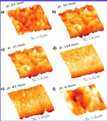
the glass transition temperature. Such transformation leads to a crystalline phase leading to a dramatic increase in hole mobility. Since the maximum photocurrent generated in a bilayer solar cell largely depends on the excitons dissociated at the active layers, monitoring the D-A interface is of utmost importance. To investigate the applicability of these polymers in bilayer solar cells, the investigation on their morphology with annealing temperature was carried out. Figure 2 shows the atomic force microscopy images of F8T2 layers annealed at various temper-atures. The annealing of the films was carried out on a digitally controlled hot plate in a nitrogen-filled glovebox. The temper-ature was varied from room tempertemper-ature to 300°C. As can be seen from the images, the as-cast F8T2 layers (Figure 2a) are fairly smooth and featureless. However, as the annealing temperature increased, it was observed that the surface roughness was also increased. (Figure 2b to 2e). It is well-known that the liquid crystal polymers align in a chain-like feature as the annealing temperature reaches 200-250 °C.13 In our case, it was observed for the films annealed at 200 and 225°C that the F8T2 layers form an ID structure with a periodic pattern and the results can be seen in Figure 2, panels d and e. It is known that the melting temperature of these copolymers is around 260 °C.22Hence, the annealing beyond this temperature will soften the films and the ID structure vanishes, resulting in a featureless smooth surface (Figure 2f). It has been found that the root-mean-square (rms) roughness value increases from 0.9 to 8.0 nm as the annealing temperature was increased from room temperature to 200°C. The roughness analysis of the F8T2 films has also been done previously by X-ray reflectivity measure-ments which have shown an increased trend in surface roughness values with an increase in annealing temperature.23 Most importantly, as explained previously, ideal bilayer structure should have ID features with a peak-to-peak distance that is comparable to or less than two times the exciton diffusion length (LD). From panels d and e of Figure 2, it was found that a clear ID structure with maximum Zmax was observed. Larger Zmax
Figure 2. Atomic force microscopy images of F8T2 thin films annealed
at different temperatures: (a) as cast, (b) 100°C, (c) 150 °C, (d) 200 °C, (e) 225 °C, (and f) 300 °C.
values result in larger roughness of the surface. A peak-to-crest height difference of the pristine and the annealed films is shown in the Supporting Information (Figure S1), which depicts a considerable increase in the roughness of the annealed films. As shown in Figure S1 (Supporting Information), the height difference between peak-to-crest in the case of the annealed films is about 25 nm, which is nearly 6 times higher than that of the pristine films. This indeed denotes the increase in the interface area for the dissociation. Overall, such regular periodic patterns of the morphology throughout the films favor the maximum interface area for the exciton dissociation.
Structural ordering observed through AFM analysis is further confirmed through X-ray diffraction experiments. The XRD data are shown in Figure 3a for the F8T2 thin films annealed at different temperatures. Upon annealing, diffraction peaks cor-responding to the (100) plane emerge, the intensity of which increase with an increase in annealing temperature. However, the diffraction intensity was visible only when the annealing temperature was higher than the glass transition temperature of the copolymer (130°C). The diffraction peak at 2θ ) 5.81° confirms the crystalline nature of the films. Crystallinity prevailed as long as the annealing temperature was well below the melting temperature of the polymer. However, when the annealing temperature exceeded the melting point of the polymer (260°C) the crystallinity vanished as shown in the figure. Hence the F8T2 undergoes a transformation from liquid crystalline state to isotropic state, leading to a disordered state.16Extraction of the crystallite size of the nanocrystals with use of the Debye-Scherrer formula resulted in a crystallite size of∼25 nm. High crystallinity with large crystal sizes is highly desirable for the high mobility of the F8T2 as discussed in the subsequent sections. Overall, the annealing temperature helps in improving the mesoscopic ordering and crystallinity which eventually maximizes the intermolecular π-π stacking.22Another striking feature that is apparent in the XRD is the shift in the (100) orientation toward higher 2θ values with an increase in annealing temperature of the films. The interplanar distance was calculated
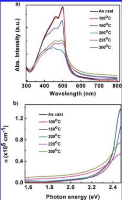
from the position of the peak and was found to be∼16 Å for the as-cast films, which is consistent with the earlier reported values.23However, with an increase in annealing temperature, it decreases to 15.4 Å. Such structural modifications reflected in the transport properties and the variation of mobility of the polymer films as a function of temperature are depicted in Figure 3b. Enhanced molecular ordering resulting in better field effect mobilities has been demonstrated previously24and similar results were also obtained in the present study. As shown in Figure 3b, the field-effect mobility showed an increasing trend with an increase in annealing temperature, with a maximum value of 1× 10⁻³cm2/(V s) at 200°C. Balanced charge transport is required for achieving high efficiencies and it has already been demonstrated previously in bulk heterojunction systems.25 In the present case, it was observed that the room temperature field effect mobility value of the active layer components F8T2 and C70measured in field-effect geometry was 1× 10⁻⁵and 1× 10⁻³ cm-2 V-1 S-1. However, when the active layers were annealed at different temperatures, the mobility values change accordingly and it was observed that at 200°C, the difference in mobility values between the two was marginal. The field effect mobilities were 1× 10⁻³and 5× 10⁻³cm-2V-1S-1 for the F8T2 and C70TFTs, respectively. Such balanced carrier transport is expected to lead to high performance of the devices. As seen from the XRD, better chain packing is apparent in F8T2 at elevated temperatures. In addition, thermal annealing of the films leads to measurable changes in the absorption spectrum. As is well-known, F8T2 is a wide band gap copolymer with an optical band gap of ∼2.4 eV at room temperature.26 Measurable shifts in the absorption edge were observed as a result of thermal annealing. Figure 4a shows the normalized absorbance of the F8T2 thin films annealed at various temper-atures. UV visible absorption maxima occurred in the wave-length range 450 to 490 nm. Appreciable reduction in the absorption occurred upon annealing, which could be attributed
Figure 3. (a) X-ray diffraction pattern of F8T2 thin films (inset:
Chemical structure of F8T2). (b) Field effect mobility of F8T2 thin
films annealed at different temperatures. Figure 4. (a) Absorption spectra of F8T2 thin films annealed at
different temperatures. (b) Variation of absorption coefficient as a function of photon energy at different temperatures.
to better chain packing. Annealing the films beyond the liquid crystal phase resulted in an increase in absorbance as the amorphous phase contributes to the absorption.27 Another striking feature of the absorption spectra is the shift in the absorption edge that occurred due to thermal treatment (Figure 4b). A shift in the absorption edge toward lower energy values with an increase in temperature was observed, which can be considered as the possible influential parameter affecting the open circuit voltage of the devices. Such a shift in absorption edges with changes in the thermal ambience of the polymer films has also been discussed in the literature in P3HT:PCBM based solar cells.28
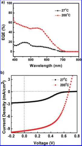
One of the mandatory conditions for achieving highest efficiencies in either bulk heterojunction or bilayer solar cells is the annealing treatment of the active layers. Figure 5a displays the EQE spectrum of the as-deposited and annealed devices. All the devices were optimized individually and it has been found that the thermally annealed devices at 200°C lead to higher EQE and higher short-circuit current density (Figure 5b) than the untreated devices. Light harvesting in the wavelength regime 400 to 600 nm is clearly visible from the EQE spectra, primarily due to the complementary nature of F8T2 and C70 fullerene active layers. And the contribution of F8T2 layers to the EQE is observed in the wavelength range 450 to 490 nm. The large value of the EQE in annealed bilayer devices originates from the efficient exciton dissociation at the F8T2/ C70interface. Moreover, thermal annealing induces enhanced self-assembly of the polymer chains, which enhances the degree of crystallinity of the polymers, thereby increasing the charge mobility as well as the overall charge transport within the system. Hence, annealing of the polymer layer, which is crucial
in achieving the desired interdigitate structure of the polymer layer, helps in achieving higher EQE signals from the devices. Electrical characteristics of the device with a geometry of ITO/PEDOT:PSS/F8T2/C70/Al are presented in Figure 5b. Under the illumination of AM 1.5 radiation (input power ) 100 mW/ cm2), the devices exhibit a short current density (J
sc) of 9.55 mA/cm2, an open circuit voltage (V
oc) of 0.67 V, a fill factor (FF) of 0.53, and a power conversion efficiency of 3.4%. At this point, it is worth mentioning that the PCE obtained in the bilayer configuration is much higher than those obtained in bulk heterojunction form. Authors have previously reported F8T2: PC70BM blend solar cells with a PCE of 2%.29 Enhanced performance of the device in bilayer configuration could be attributed to the nanostructured ID structures of the F8T2 polymer layers as well as their balanced mobility with the C70. Variation of device parameters as a function of annealing temperature is also depicted in Table 1. It was observed that the devices with annealed active layers at 200°C have a roughly 4-fold increase in current density compared to nonannealed devices. For the as-deposited devices, series resistance was found to be large and hence resulted in poor fill factor and PCE. Moreover, the interface of the bilayer films is not well-defined and there is hardly any intermixing of the layers at the interface leading to poor interface. As the annealing temperature was increased, the intermixing of the layers as well as the interface area has increased due to the morphological changes that occurred in the polymer films as shown in Figure 2c. These morphological changes create a larger interface area for the exciton dissociation, thereby increasing the photogeneration. There was a systematic increase in the current density with the increase in anneal temperature that reaches a maximum value of 9.55 mA/cm2at 200 °C, and further heating leads to the degradation of the device performance because of the deteriora-tion of the ID structure. Polymers tend to crystallize at high temperature and the high-temperature annealing leads to inter-chain aggregation, which will result in increased mobility of the polymer as explained previously. As a result increased mobility is anticipated as seen in Figure 3, which can eventually result in higher current densities. However, annealing did not help in increasing the open circuit voltage. It was shown that the open circuit voltage decreases from 0.9 to 0.67 V as the annealing temperature increased from room temperature to 200 °C. It was observed that the absorption edge of the F8T2 molecule shifts to lower energy (Figure 4). Correspondingly, the highest occupied molecular orbital (HOMO) of the F8T2 polymer becomes altered resulting in the reduction in open circuit voltage at elevated temperatures. Such a behavior was also observed previously in P3HT/PCBM28and MEH-PPV/C
60 systems.30 It is also worth mentioning that the fill factor drastically improves and reaches a maximum value of 0.53 as the annealing temperature reached 200°C. The dependence of device performance on the annealing temperature is associated with the morphological evolution of the active layers as seen
Figure 5. (a) External quantum efficiency and (b) I-V characteristics
obtained under white light radiation, AM 1.5 (100 mW cm-2), for as fabricated and annealed devices.
TABLE 1: Summary of Device Parameters for the F8T2/C70
Bilayer Devices Annealed at Different Temperatures
annealing temp (°c) rms roughness (nm) Voc(V) FF Jsc (mA/cm2) η (%) 27 0.76 0.55 0.28 2.60 0.40 100 0.81 0.76 0.43 3.07 1.20 150 1.17 0.93 0.43 3.56 1.40 200 8.55 0.67 0.53 9.55 3.40 225 2.33 0.61 0.50 9.20 3.30 300 0.25 0.40 0.24 1.20 0.11
from the AFM images. A nearly 9-fold increase in efficiency of the devices upon annealing is therefore attributed to effective exciton dissociation and balanced charge transport. Further enhancement in efficiency could be anticipated by the optimiza-tion of the individual layer thickness or through better light harvesting through various material combinations. Use of exciton blocking layers could also partially help to improve the overall efficiency of the devices. Performance of the devices can be further enhanced through proper device architectures which include tandem and cascade structures. Since F8T2 is a wide band gap copolymer, it utilizes only 30% of the visible light when compared to the P3HT polymers, which utilize about 45% of the spectrum. Since the absorption of the F8T2 polymer occurs in the narrow wavelength regime of 450 to 490 nm, it can be used for complementary spectrum coverage with materi-als of varying bandgaps, which can further improve the overall efficiencies. Overall, the bilayer configuration offers more flexibility in the choice of materials because of the fact that there is no need for formation of complex percolation paths which are a bottleneck in the bulk heterojunction.
Conclusion
In conclusion, morphology-dependent device performance of the F8T2/C70bilayer solar cells is presented. The high efficiency observed in the bilayer structure is largely associated with the rougher morphology of the F8T2 polymer and balanced charge transport. Annealing temperatures leading to a well-aligned liquid crystal phase of the polymer result in a significant increase in the current density values as well as the overall efficiency of the devices. Utilizing F8T2 copolymer with variable morphology has been successfully demonstrated in the area of bilayer solar cells through their integration with fullerene C70as acceptors for the accomplishment of devices with power conversion efficiencies of 3.4((0.2)%. Since the wider band gap of F8T2 allows the absorption below 500 nm, it would be ideal to integrate it with low band gap materials to utilize the solar spectrum effectively.
Acknowledgment. The authors acknowledge the financial support from the National Science Council, Taiwan (96-2221-E-001-017-MY2), and Academia Sinica, Taiwan.
Supporting Information Available: Figure S1 showing the roughness analysis of F8T2 thin films. This material is available free of charge via the Internet at http://pubs.acs.org.
References and Notes
(1) Tang, A. J. Appl. Phys. Lett. 1986, 48, 183.
(2) Yang, F.; Shtein, M.; Forrest, S. R. Nat. Mater. 2005, 4, 37–41. (3) Chu, C. W.; Shao, Y.; Shrotriya, V.; Yang, Y. Appl. Phys. Lett.
2005, 86, 243506.
(4) Peumans, P.; Uchida, S.; Forrest, S. R. Nature 2003, 425, 158. (5) Xue, J.; Uchida, S.; Rand, B. P.; Forrest, S. R. Appl. Phys. Lett.
2004, 84, 3013.
(6) Law, M.; Greene, L. E.; Johnson, J. C.; Saykally, R.; Yang, P.
Nat. Mater. 2005, 4, 455.
(7) Greene, L. E.; Law, M.; Yuhas, B. D.; Yang, P. J. Phys. Chem. C
2007, 111, 18451.
(8) Boucle, J.; Ravirajan, P.; Nelson, J. J. Mater. Chem. 2007, 17, 3141. (9) Yang, F.; Shtein, M.; Forrest, S. R. J. Appl. Phys. 2005, 98, 014906. (10) Fujiwara, T.; Locklin, J.; Bao, Z. Appl. Phys. Lett. 2007, 90, 232108. (11) Li, S. P.; Newsome, C. J.; Russell, D. M.; Kugler, T.; Ishida, M.; Shimoda, T. Appl. Phys. Lett. 2005, 87, 062101.
(12) Chua, L. L.; Zaumseil, J.; Chang, J. F.; Ou, E. C. W.; Ho, P. K. H.; Sirringhaus, H.; Friend, R. H. Nature 2005, 434, 194.
(13) Huang, J. H.; Yang, C. Y.; Ho, Z. Y.; Kekuda, D.; Wu, M. C.; Chien, F. C.; Chen, P.; Chu, C. W.; Ho, K. C. Org. Electron. 2009, 10, 27. (14) Peet, J.; Kim, J. Y.; Coates, N. E.; Ma, W. L.; Moses, D.; Heeger, A. J.; Bazan, G. C. Nat. Mater. 2007, 6, 497.
(15) Zhang, F.; Jespersen, K. G.; Bjo¨rstro¨m, C.; Svensson, M.; Ander-sson, M. R.; Sundstro¨m, V.; MagnuAnder-sson, K.; Moons, E.; Yartsev, A.; Ingana¨s, O. AdV. Funct. Mater. 2006, 16, 667.
(16) Grell, M.; Bradley, D. C.; Inbasekaran, M.; Woo, E. P. AdV. Mater.
1997, 9, 798.
(17) McGehee, M. D. Mater. Res. Soc. Bull. 2009, 34, 95.
(18) Sirringhaus, H.; Kawase, T.; Friend, R. H.; Shimoda, T.; Inbaseka-ran, M.; Wu, W.; Woo, E. P. Science 2000, 290, 2123.
(19) Breeze, A. J.; Schlesinger, Z.; Carter, S. A. Phys. ReV. B 2001, 64, 125205.
(20) Kim, Y. G.; Walker, J.; Samuelson, L. A.; Kumar, J. Nano Lett.
2003, 3, 523.
(21) Ravirajan, P.; Haque, S. A.; Durrant, J. R.; Bradley, D. C.; Nelson, J. AdV. Funct. Mater. 2005, 15, 609.
(22) Pattison, L. R.; Hexemer, A.; Kramer, E. J.; Krishnan, S.; Petroff, P. M.; Fischer, D. A. Macromolecules 2006, 39, 2225.
(23) Werzer, O.; Matoy, K.; Strohriegl, P.; Resel, R. Thin Solid Films
2007, 515, 5601.
(24) Laquindanum, J. G.; Katz, H. E.; Lovinger, A. J.; Dodabalapur, A.
AdV. Mater. 1997, 9, 36.
(25) Li, G.; Shrotriya, V.; Huang, J.; Yao, Y.; Moriarty, T.; Emery, K.; Yang, Y. Nat. Mater. 2005, 4, 864.
(26) Deng, Y. Y.; Sirringhaus, H. Phys. ReV. B 2005, 72, 045207. (27) Gather, M. C.; Bradley, D. C. AdV. Funct. Mater. 2007, 17, 479. (28) Chu, C. W.; Yang, H.; Hou, W. J.; Huang, J.; Li, G.; Yang, Y.
Appl. Phys. Lett. 2008, 92, 103306.
(29) Huang, J. H.; Lee, C. P.; Ho, Z. Y.; Kekuda, D.; Chu, C. W.; Ho, K. C. Sol. Energy Mater. Sol. CellsIn press.
(30) Drees, M.; Premaratne, K.; Graupner, W.; Heflin, J. R.; Davis, R. M.; Marciu, D.; Miller, M. Appl. Phys. Lett. 2002, 81, 4607. JP910023D