716 J. Elect rochem. Soc., Vol. 143, No. 2, February 1996 The Electrochemical Society, Inc. Manuscript submitted April 28, 1995; revised
manu-script received Oct. 5, 1995.
Sophia University assisted in meeting the publication costs of this article.
REFERENCES
1. R. D. Westbrook, B. F Wood, and G. E. Jellison, Jr.,
Appl. Phys. Lett., 50, 469 (1987).
2. A. Yoshida and K. Setsune, IEEE Electron Devices
Lett., EDL-9, 90 (1988).
3. A. Yoshida, M. Kitagawa, K. Setsune, and T. Hirao, J.
J. Appi. Phys., 27, L1355 (1988).
4. M. Kitagawa, N. Matsuo, G. Fuse, H. Iwasaki, A.
Yoshida, and T. Hirao, ibid., 27, L2139 (1988).
5. G. Kawachi, T Aoyama, K. Miyata, Y. Ohno, A.
Mimura, N. Konishi, and Y. Mochizuki, This Journal, 137, 3522 (1990).
6. G. Kawachi, T. Aoyama, T. Suzuki, A. Mimura, Y.
Ohno, N. Konishi, Y Mochizuki, and K. Miyata, Jpn.
J. Appl. Phys., 29, L2370 (1990).
7. K. Masumo, M. Kunigita, S. Takafuji, N. Nakamura,
A. Iwasaki, and M. Yuki, ibid., 29, L2377 (1990).
8. A. Mimura, G. Kawachi, T. Aoyama, T. Suzuki, Y.
Nagae, N. Konishi, and Y. Mochizuki, IEEE Trans.
Electron Devices, ED-40, 523 (1993).
9. G. Kawachi, T. Aoyama, A. Mimura, and N. Konishi,
Jpn. J. Appl. Phys., 33, 2092 (1994).
10. B. Mizuno, I. Nakayama, N. Aoi, M. Kubota, and T.
Komeda, Appi. Phys. Lett., 53, 2059 (1988).
11. C. Yu and N. W. Cheung, IEEE Electron Device Lett.,
EDL-15, 196 (1994).
12. J. Nishizawa, K. Aoki, and T. Akamine, Appl. Phys.
Lett., 56, 1334 (1990).
13. S. Matsumoto, S. Yoshioka, J. Wada, S. Imai, and K.
Uwasawa, J. Appi. Phys., 67, 7204 (1990).
14. X. Y. Qian, N. W. Cheung, and M. A. Lieberman, Appl. Phys. Lett., 59, 348 (1991).
15. T. Inada, A. Kuranouchi, H. Hirano, T. Nakamura, Y.
Kiyota, and Y. Onai, ibid., 58, 1748 (1991).
16. T. Hara, S. Nakagawa, K. Shinada, and S. Nakamura,
ibid., 63, 90 (1993).
17. T. Hara, K. Shinada, and S. Nakamura, Jpn J. Appl.
Phys., 33, 5608 (1994).
18. A. Hasegawa, B. I. Kang, and K. Shono, Trans. IEICE
Jpn., J75-C-II, 28 (1992).
19. A. Hasegawa, R. I. Kang, and K. Shono, in
Proceed-ings of 1992 IEEE International Conference on
Semiconductor Electronics, Malaysia, p. 213, IEEE
(1992).
20. F. N. Smits, BSTJ, 36, 711 (1958).
21. B. Mcdonald and A. Goetsberger, This Journal, 109,
141 (1962).
22. S. D. Rosenbaum, Solid-State Electron., 11, 711 (1968).
23. J. C. Irvin, BSTJ, 41, 387 (1962).
24. C. T. Sah and H. C. Pao, IEEE Trans. Electron Devices,
ED-13,393(1966).
25. W Kern and D. A. Puotinen, RCA Rev., 31, 187 (1970). 26. Y.-C. Tseng and K. Shono, Jpn. J. Appl. Phys., 28, L329
(1989).
27. Y.-C. Tseng and K. Shono, ibid., 30, L222 (1991).
28. 0. Kudoh, K. Nakamura, and M. Kamoshida, J. Appl.
Phys., 45, 4514 (1974).
29. J. R. Brews, IEEE Trans. Electron Devices, ED-26, 1696 (1979).
Modeling of the Wear Mechanism during
Chemical-Mechanical Polishing
Chi-Wen Liu,0 Bau-Tong Dai,b Wei-Tsu Tseng,b and Ching-Fa Yeh°
Departmentof Electronics Engineering and Institute of Electronics, National Chiao Tung University, Hsinchu, Taiwan bNational Nano Device Laboratory, Hsinchu, Taiwan
ABSTRACT
A model based on statistical method and elastic theory is presented to describe the wear mechanism of the silicon wafer surface during chemical-mechanical polishing. This model concerns the effects of applied pressure and relative velocity between the pad and the wafer on the removal rate during polishing and is capable of delineating the role of the mechanical properties of the slurry particles and the films to be polished. The removal rate is dependent on the elastic moduli of slurry particle and polished film. Comparisons with experimental data demonstrate the validity of the model for predicting relative removal rate for various dielectric films.
Introduction
The increasing complexity of device designs and the
emergence of deep submicrometer structures require min-imum surface topographies for future lithography
require-ments in the integrated circuit (IC) industry. Surface topographies are reduced using advanced planarization processes like thermal flow, bias-sputtered dielectrics, etchback, and spin-on glass.13 However, it is generally agreed that conventional techniques merely smooth the
topography locally and have no significant effect on
glob-al planarization. A new planarization method, cglob-alled
chemical-mechanical polishing (CMP), has become widely
accepted for planarizing interlevel dielectrics4 and for
selective removal of aluminum,6 tungsten,67 copper,7 and titanium° overburden following metal filling of studs and interconnects.
CMP involves simultaneous and intimate contact
between the wafer surface and a pad charged with a layer of colloidal silica slurry. The relative motion between the wafer and pad, combined with applied pressure and chem-ical activity of the slurry results in abrasion of the wafer
surface. Specifically, when a particle embedded in the fibers of the pad has sufficient strength and energy to overcome the fracture toughness of polished material, strikes the wafer surface, material is removed from the
surface. Unfortunately, it is difficult to design experiments to separate out the effects of a particular consumable from
other controlled variables that affect the removal rate,
such as the type of pad, film properties, slurry
characteri-zation, and pad conditioning. Hence, not many details
about CMP removal mechanisms are available. This lack
of understanding of polishing mechanics and chemistry
sets limits on the ability of experimentally based statisti-cal methods to improve the process, and is a major draw-back to adopting CMP for manufacturing. Consequently, a wear model is urgently needed to upgrade understanding of CMP removal mechanisms, and to relate process para-meters to actual material removal.
To better understand the polishing physics from various science and engineering fields, wafer-scale and feature-scale physics have been modeled by various researchers. The most common wafer-scale model for material removal is Preston's equation,1° where removal rate of material is
J. Elect rochem. Soc., VoL 143, No.2, February 1996 The Electrochemical Society, Inc. 717 related to the work per unit time done on each unit area of
the surface to be polished. Cook" reviewed the mechanics and chemical polish of glass polishing, which has signifi-cant association with CMP of silicon dioxide. In his analy-sis, a microcutting mechanism was proposed to simulate the breaking of chemical bonds which result from interac-tion of both the glass surface and polishing particle with water. From the field of tribology, Runnels and Eyman" analyzed the behavior of the fluid film between the wafer and the pad. Hydrodynamic lubrication is, however, only responsible for distributing the slurry, and rnicrocutting of polished film due to solid-solid contact has not been used to characterize the process.
Burke' introduced a semiempirical model of Si02 pol-ishing, and gave insights into the effects of "down" area dimensions, "up" area patterning, and feature step height.
Warnock'3 presented a phenomenological model that
describes the CMP process. This model, which intuitively
assumes partial wafer-pad contact, can predict erosion
profile of array of features with different sizes and pattern density. Runnels'4 proposed a feature-scale model for pol-ishing using a hydrodynamic slurry layer that bridges the
gap between wafer- and particle-scale models through layer-thickness and erosion laws. Another modeling approach1' assumed that material removal is related to
"sharp edges," which are defined as slurry particles
embedded in the fibers of the polishing pad that have suf-ficient force to increase their effective masses to the point where polishing can occur. Thus, distribution of effective sharp edges determines the removal rate and uniformity of polished surface. All the above models, however, have not
proven satisfactory enough at distinguishing among
consumables which affect removal rates. There is still a
need to develop models for fundamental understanding
of the process that can be used as a base for process
development.
In the CMP process the real contact area between slurry
particles and the wafer surface, that dominates the
removal of material from the wafer surface, is different for various combinations of dielectric films and slurry parti-cles due to their differing surface mechanical properties. Therefore, knowledge of the contact area, wafer surface mechanical properties, and slurry particle characteristics is critical in determining the removal-rate predictions. So far, little has been reported on this subject. For this reason, wear analysis was performed to enhance our
understand-ing of wafer-surface/slurry-particle contact mechanics
during the CMP process. Our previous work'6 reported a
linear relationship between removal rate and film
hard-ness. Cook's review" proposed a 1/modulus-dependence removal rate. Therefore, one may intuitively correlate the removal rate with a "mechanical factor" of hardness/mod-ulus as we pointed out previously.'6 We describe here a more complete erosion model based on statistical mecha-nism and elastic theory which fits removal rates for dielec-tric films. This allows quantitative evaluation of a given CMP process and provides a basis for process optimization to meet specific technological requirements, such as
selec-tive polishing processes.
Experimental
Preparation of dielectric films.—All test samples were
prepared on p-type (100), 150 mm silicon wafers.
Thermally grown silicon dioxide films were obtained by wet oxidation (ASM/LB45 furnace system), in which the silicon was exposed to an ambient of 112 and 0, at 980°C.
Films of plasma-enhanced chemical-vapor deposition
(PECVD) oxide were deposited with the AMT/P5000 sys-tem, tetraethylorthosilicate (TEOS) and 0, at 390°C were used as a reactant gas for TEOS-PECVD films; SiH4, N2, and NH3 at 400°C for deposition of Si3N4-PECVD films. Silicon-rich oxide (SRO-PECVD) films were obtained in
ambient SiH4, N2, and N20 at 400°C with a Novellus reactor. All! specimens were deposited to a thickness of —1 m.
Polisher setup.—A Westech Model 372M CMP processor,
consisting of an IC 1000/Suba IV (made of polyurethane
impregnated polyester) pad affixed to a circular polishing
table and a carrier to hold wafers against the pad, was used for polishing. During the polish experiment, the wafer was mounted on a template assembly for a single 6 in. diam wafer. The Teflon retaining ring is recessed from the wafer surface by 7 mil. Pressure at the
wafer-slurry-pad interface is controlled via an overhead
mecha-nism which allows pressure to be applied to the wafer
holder. Both the carrier and table were rotated indepen-dently. The thickness of the dielectric film was measured
with Nanometrics 2100XP by a 10 mm edge exclusion, and
was averaged over nine different locations on the wafer to determine the polish rate. Cross-wafer nonuniformity of
the dielectric polish rate was less than 10%. The polish slurry (SC-i slurry available from Rippey Corp.) was a
suspension of fumed silica dispersed in aqueous potassium hydroxide. To allow for removal-rate variations from run to run, the removal rate ratio (R. R. ratio) is defined as
Removal rate of dielectric film
R.R.ratzo
Removal rate of thermal oxide Pad conditioning.—Pad conditioning techniques were used to refurbish the pad surface to maintain the removal
rate without sacrificing uniformity. In our experiments, pad conditioning with Rotating Pad Conditioner II was
performed between each wafer to clean the slurry residue and to lift the pad fibers for further processing. Without
this procedure, the polish rate decreased substantially after only several wafers. Our polish experiments were
carried out under well-controlled conditions, as described
in our previous study,'6 e.g., pad conditioning was
per-formed before and between each wafer, and polishing was
terminated before pad glazing could cause significant
decrease in removal rate.
Nanoindentation measurement.—Young's modulus data
were determined using the NanoTest 500 mechanical
properties microprobe developed at Micro Materials Ltd.
(UK). Nanoindentation loads are applied through a coil
and magnet assembly. The position of the indenter is mea-sured by capacitive sensors. The indenter probe is a three-sided pyramid (Berkovich) which projects an equilateral triangle on the sample. Theoretically, the area can be
cal-culated if the displacement is known. At very shallow
depths, the tip of the indenter is not perfect, so the
depth-to-area relationship was calibrated with fused silica,"8 since it has a very smooth surface and isotropic elastic
properties. Thus precise reproducible data can be obtained
at shallow depths without having to image the indent.
Here, the loading rate was set at 1.18 mN/s to a maximum depth of 300 nm and the ambient temperature was held at 22.7°C. We assumed that the substrate did not significant-ly affect the modulus value obtained by indenting into the first 300 nm of the 1 m thick films. For each sample, ten
separate indents, spaced 15 p.m from each other, were
made on the surface under investigation. Modeling
Tobegin with, we consider the process of rolling as an analogy to the CMP removal mechanism in which wafers are being pressed down against the pad, and slurry parti-cles are moving in the gap between the wafer and the pad in a shearing (cutting) action. Kragelsky at at." proposed the kinematics of an abrasive particle moving in the gap of
a rolling-contact pair. From statistical mechanism, they
assumed (i) the velocity v of the abrasive particle is a lin-ear combination of the velocities of the two surfaces v, and
v,, respectively, i.e.
V = av,+ 3v, [1]
where and 13 are the probability of adherence of the par-ticles to surface 1 and surface 2, respectively, mean values
of which can be assumed to be approximately inversely proportional to the Brinell hardness values of surface
718 J. Electrochem. Soc., Vol. 143, No.2, February 1996 The Electrochemical Society, Inc. SB2 SB, +SB,, 13 SB, SB, +SB,,
rsa
d Ca+l31
[4](ii)A spherical model of a particle of diameter 22 under
uniform load F penetrates the two mated surfaces. The depth of penetration of the particle into the two mated
surfaces depends on the surface hardness of the particle and of the two mated surfaces. (iii) Abrasive particles do not rupture in the load-contact range until the maximum
depth of penetration into the surface materials
corre-sponds to rupture strength of the particles.
From the above simplification, the time t of contact of
abrasive particle in the gap between the mated surfaces
from the point of its introduction into the gap to the point,
where it attains a depth of penetration (h, for surface 1
and Ii,, for surface 2), can be given by'9 Fig. 1. Schematic representation for the settling of the slurry
par-ticleinto the gap betweenthe surface of the wafer and the pad.
=
(forsurface 1)R [HB2av,+13v,,j
=fJwB,+SB2)h,1
(for surface 2) [5] 2 [SB, (ctv, + l3v,,)J where [6] P,+P,p, and P2arethe radii of curvature of surface 1 and
sur-face 2, respectively.
During the interval of time t, the abrasive particle moves in the gap between the mated surfaces with ever-increas-ing penetration into the contact materials and deforms a certain volume G of the surface material. The deformed volume can be expressed as"
Fig. 2. Schematic representation of the contact between slurry pa(le (of radius RJ and wafer surface performed by moving the slurry particle on the wafer surface from the engagement point (point c) to a depth of penetration c into the wafer.
G =
jT (k)5/2[
SB, 1V (for surface 1)[(av, +13v2)522
i
=
\/
(h,,)" 1122 1V (for surface 2) [7] [(av, +(3v,,)SB, jwhereV =lv,—
v,,lis the relative velocity between surface 1 and surface 2.
CMP is a method of planarization where the wafer is
pressed facedown by a carrier and rotated against a pol-ishing pad covered with a layer of slurry. The pad is used to hold the slurry particles, transmit load forces to the
par-tide/wafer surface, and conform precisely to the film
being polished. A schematic representation of the settling of the slurry particle into the gap between the surface of the wafer and the pad is illustrated in Fig. 1. Since the role of hydrodynamic lubrication of the fluid film is
distribut-ing the slurry,12 lowerdistribut-ing friction force, and removdistribut-ing
slurry particles are in direct contact with both the pad and
the surface of the wafer during the polishing process. Since hardness is a determining factor in how deeply a
abraded chips and heat generated by the CMP process, the
particle (slurry-carried particles in the case of CMP)
pen-etrates into a surface, the harder the deformed material,
the less it is penetrated under a given load. Thus, the depth of penetration into the pad surface (made of polyurethane
which is softer) was assumed to be greater than into the
surface of the wafer as schematically shown in Fig. 1.
During CMF the slurry particles move between the
wafer and the pad. Figure 2 is a schematic representation of the slurry-particle/wafer-surface system in which
slur-ry particle moves along the wafer surface from
engage-meat point (point c) into the wafer to the depth of
pene-tration äd. Local pressure at the point of contact in the
system is at times largely determined by the nature of the polishing lap. Thus, the microvolumes Gae, on the contact
surfaces as shown in Fig. 3 undergo elastic and plastic deformation or microcutting depending on the depth of penetration. The conditions for these deformations are
determined by certain transition criteria,1' i.e., h,,, the
cri-tenon for transition from elastic to plastic deformation
and hpm, the criterion for the transition from plastic
defor-mation to microcutting. By means of these criteria, the deformed volumes can be separated into three regions (Fig. 3), e.g., regions of elastic deformation Ge, plastic
deformation G, and microcutting G".
b
a
fig.3. Regions of elastic deformation G, plastic deformations G,
and microcutting Gm from the introduction point (paint c)of slurry particle to a depth of penetration a.
J. Elect rochem. Soc., Vol. 143, No.2, February 1996 The Electrochemical Society, Inc. 719 Generally, ceramic materials such as SiO, and Si3N4
have an insufficient number of independent slip systems
by which general deformation can occur and may have
structures that are so complex dislocation motion is diffi-cult.2° Thus, on loading the surface of a dielectric by an
indenting particle, deformation is directly transformed __________ fromelastic deformation to microcutting with little or no
intermediate transitional time. Only a limited amount of plastic deformation is possible in this process. Also, since
the elastic deformation occurs at low load levels, the
deformation volume is small compared with the volume of microcutting due to overloading. We assumed therefore the deformation volume during contact time to be approx-imately equal to the volume of microcutting, i.e.
Gabcd= Gm>> G + G" ___________
Dividingthe deformed volume GbCdbythe contact time t, the removal rate (R. R.) can thus be obtained
1)
h'R°'V
HV23)
HV+HV,
h"R°'V HV,,, HV,, + HV,,. (h)"2 VI
HV
3where the Vickers' hardness numbers (HV) are used for thin films and the surfaces of the wafer and of the pad cor-respond to surface 2 and surface 1, respectively; e.g.
h,=h HV2=HV HV1=HV
The real contact area Ak as assumed by Kragelsky et at." can be expressed in terms of radius R and depth of pene-tration od = h of the slurry particle, hence
Ak 2irRh
The problem now becomes how to determine the depth of penetration h. Let us consider a case in which two elas-tic bodies, say, two balls, are pressed against each other by
external forces. The pressure is distributed over a small
circle of contact formed as a result of local deformation. The radius r of the contact circle is given by the elasticity
equation proposed by Hertz21
=088[F(E2+E,)d213 L2E,E,(d,+d3)] [8] R.R. Gab,d
t
[9]Thus, the real contact area AH from Hertz's theory can be expressed as
AH
=ir 0.881F +Ew)R13 [16]
[
2ESE,I
The real contact area, calculated either according to
Kragelsky et at." or to Hertz,2' should be equal, i.e.
Ak = A,, [17] Thus, 12
(F(E +E )R'
2rRh = r 0.88 2ESEW J [18]Depth of penetration h is thus calculated as
IE
+E F
h=C
L ESEWJ/J
[19]where C is a constant. Substituting Eq. 19 into Eq. 9
R.R.=CAI HV 1+EwYv
(HV+HV) E,E )A)
( HV
I ii PV [20]HV+HV) EE )
where A is the area of the wafer. C' also contains the
chem-ical effect which is perceived as being independent from mechanical factors and is constant assuming fixed slurry chemistry. Equation 20 indicates that surface mechanical
properties of the wafer, the pad, and the slurry particle,
such as hardness and Young's modulus, play significant roles in the polishing rate. When other controlled variables are fixed, Eq. 20 predicts that removal rate will decrease with increasing pad hardness, which is in agreement with previous reports."
Generally, the wafer surface is hard and brittle, while the pad, typically polyurethane-based materials, is much
softer, i.e., HV <<NV,,,. Hence removal rate can be
simpli-fied to
R.R. = C,1EEPV
E,E,,, ) =C'I-_-+-±PV
[21]E, E)
[10] [11]P
[12]where E2 and E, are the moduli of the two balls and d, and d, the corresponding radius; F is applied force.
Similarly, a slurry particle penetrates a flat dielectric
plane with R, radius of curvature due to force applied to the slurry-particle/wafer-surface system (Fig. 4). Hence,
the radius r of the contact circle derived from the
Hertizian theory can be approximated byEF(E + E )RR 13
r=O.881 W f
[13]
[2E,E(R+R,) j
where the surface of the wafer and the slurry particle are equal to ball 2 and ball 3, respectively, namely
E2 = E,,, E, = E, d, =R, d, = R [14] Assuming the wafer surface to be a plane surface, R, is
thus very large and R <<R,, Eq. 13 can be simplified to
r= 088[F(E+ Ew)R13
L
2E,E) J
[15]720 J. Electrochem. Soc., Vol. 143, No. 2, February 1996 The Electrochemical Society, Inc. While Eq. 21 excludes the effect of HV on the removal
rate, we do not, however, rule out the significance of pad characteristics in polishing behavior. In real cases, removal rate is very slow when smooth pads are used because the slurry particles cannot be held in the fibers of the pad.15 The influence of the surface morphology of the pad on pol-ish rate and uniformity is still an area that requires further investigation and is outside our present scope.
A wear model for the CMP process similar in form to Preston's equation has been developed and has the partic-ularity of separating out the mechanical properties of the slurry particle and the surface of the wafer from Preston's coefficient. To summarize, the kinetics of polishing are: (i) the rate of material removal is dependent on the real con-tact area between the slurry particle and the surface of the wafer. The real contact area is determined by applied pres-sure, the curvature, and Young's modulus of the slurry
par-ticle and the surface of the wafer; (ii) the removal rate increases linearly with increasing applied pressure and relative velocity between the pad and the surface of the
wafer, as in Preston's equation; and (iii) the removal rate increases as a result of a reduction in the modulus of slur-ry particle or film to be polished.
The model we developed herein relates removal rate to measurable material properties and hence provides a
sim-ple and explicit way to monitor the CMP process.
Experimental results with various dielectric films are pre-sented and discussed in the next section.
Resultsand Discussion
Effectof pressure and rotation velocity on the removal
rate of dielectric film—Our wear model, similar to
Preston's equation, suggests that material removal is
directly proportional to the applied pressure and relative rotation speed. We investigated the characteristics of the CMP process and observed that an increase in polish pres-sure and pad rotation speed promoted the removal rate,4 while carrier rotation speed, back pressure, and increased slurry flow have a less pronounced effect on the polishing
rate. We also found that adjustments in the pad and
carrier speed determine the polishing uniformity, and
that increased back pressure leads to more uniform
removal. Details about the effects of polish pressure and rotation speed on removal rate can be found in our
previous report.4
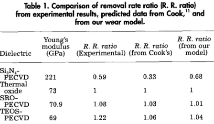
Effect of the modulus of the dielectric film on experi-mental erosion data.—To examine the role of the modulus of the dielectric film on polish rate, four kinds of dielectric film including Si3N4-PECVD film, thermal oxide,
SRO-PECVD, and TEOS-PECVD film were used. Young's
mod-uli of various dielectric films were obtained from nanoin-dentation measurements and are listed in Table I. It was clearly observed that the value of Young's modulus of the Si3N4 film, 221 GPa, was much larger than those of oxide films. This is because the basic structure of Si3N4 consists of an SiN4 tetrahedron shared by three other SiN4 tetrahe-dra to form a three-dimensional network. The Si-N bond is formed by the overlapping of the sp3 orbital of the sili-con and the sp2 orbital of the nitrogen with additional ir-bonding from the nitrogen to the empty 3d level of the sil-icon. This creates an exceptionally strong bond in Si3N4,
producing a rigid structure with a Young's modulus
greater than three times that of quartz. The oxygen atoms in the Si02 form a silicate network sharing only two tetra-hedra.22 Further, the value of modulus of the oxide film is
notably dependent on the type of precursor used and on deposition technique. This suggests that variations in
modulus of oxide films is the result of hydrogen incorpo-ration, the presence of defects, microvoids, clusters, and
dangling bonds due to various preparation processes. The
measured values of modulus of thermal oxide, SRO-PECVD, and TEOS-PECVD are 73, 70.9, and 69 GPa,
respectively, which are consistent with recent studies.22'23
As Eq. 21 predicts, removal rate is affected by the
combination of moduli of slurry particle and polished
film when other process variables are fixed. We
proceed-ed to examine two real cases involving dielectric polish processing
Oxide films polished with silica particles—Since the
PECVD oxide films and silica particles were prepared by
vapor deposition methods and have virtually the same
SiO2 network structure, it can be assumed that no differ-ence exists between the moduli of these oxides. Thus, by substituting E, =
E
into Eq. 21, the removal rate becomesRR.=C'[_]PV
[22]Equation 22 indicates that removal rate is inversely pro-portional to modulus of polished films, same as the erosion
model in Cook's review. Experimental data show good
agreement with predicted results when compared with the
removal rate and modulus for thermal oxide,
SRO-PECVD, and TEOS-PECVD films as shown in Table I.Si3N4 films polished with silica particles.—Cook's model
implies inherently equal modulus for polished films and slurry particles so that the difference in mechanical prop-erties between the "polisher" and the "polished" is ignored and its role in removal rate is underestimated. Since the modulus of Si3N4 is much larger than that of silica, the
relationship between removal rate and modulus of
pol-ished film thus should not follow Cook's model, and a large
deviation was observed as shown in Table I. Removal rate
data based on our model show a close match with the
experimental values.
As discussed above, our model presents a more general expression of removal rate (Eq. 20) which includes both hardness and modulus of the materials involved in the pol-ishing action. This model does predict the same removal
rate PV dependence as in Preston's equation and can be extended to cases where slurry and film properties are
discernible. For slurry and film with the same modulus, our model reduces to a special case of Cook's model as in
Eq. 22. For slurry and film of differing mechanical
natures, Eq. 21 weighs the contributions of the two mod-uli -and
yields a better prediction of removal rate.
Although our polish experiments were all carried out
under most stable conditions as described earlier, as much as a 15% mismatch still exists between our modeled data and the experimental data. This can be attributed to inho-mogeneity of film properties, uneven slurry distribution, temperature variations, and other transient variables.
For CMP of metal films, the desirable processes are first the formation of an insoluble and hard passivation layer on the metal surface through chemical reactions with slur-ry and then removal of the passivation layer by
mechani-cal polishing or simply "rubbing," leaving a fresh metal
surface for continuing chemical reaction, and then repeat-ing the process.6'7 In light of this proposed scenario, the removal rate may not be governed merely by mechanical actions, the chemical reaction rate may play a more sig-nificant role in the removal mechanism. In addition, the large volume of plastic deformation of metals necessitates the inclusion of the G6 term in Eq. 8, which complicates
Table 1. Comparison of removal rate ratio (R. R. ratio) from experimental results, predicted data from Cook,11 and
from ourwearmodel.
Young's modi.ilus Dielectric (GPa) R. R. ratio (Experimental) F. R. ratio (from Cook's) R. R. ratio (from our model) S13N4-PECVD 221 0.59 0.33 0.68 Thermal oxide 73 1 1 SRO-PECVD 70.9 1.08 1.03 1.01 TEOS-PECVD 69 1.22 1.06 1.04
J. E!ectrochm. Soc., Vol. 143, No. 2, February 1996 The Electrochemical Society, Inc. 721
the modeling process. In short, extension of the proposed wear model to metal CMP requires major revision and is currently under investigation by our team.
Conclusion
Anab initio wear model for CMP processing has been
developed based on kinematics and elastic theory The
model described herein has been demonstrated to possess
the ability to link process variables including applied
pressure and relative rotation speed between the polishing pad and the wafer being polished to removal rate, and has the particularity of correlating the effects of mechanical
properties of the slurry particles and polished film with
removal rate through approximation of the contact area. Increases in polishing pressure and pad speed have been
shown to promote the polish rate as predicted by our
model. However, it must be emphasized that pad glazing and inadequate pad conditioning result in degradation of removal rates due to poor slurry transport. Elastic moduli of slurry and the dielectric to be polished are shown to be
critical factors in determining the CMP removal rates.
Preliminary experimental results indicate that for slurry and dielectric with the same modulus (e.g., Si02 polished by silica), the current model reduces to a special case of Cook's model in which removal rate is inversely propor-tional to the film modulus. For dielectric and slurry with
differing mechanical properties (e.g., Si3N4 polished by
sil-ica), our model is able to sort out the effects of the two
contributing moduli and give a more faithful prediction of removal rates. Thus, the type of wear mechanism
demon-strated has the potential of not only increasing
under-standing of, but also optimizing the polishing process.
Acknowledgment
Theauthors express appreciation for helpful discussions with Dr. T. Y. Yen in the Institute of Mechanical Engineering,
National Chiao Tung University. This work is supported by UMC, TSMC, and National Science Council (N5C84-2622-E009-007), R.O.C. The Young's modulus measurements were made possible by the assistance of the Precision Instrument Development Center in providing the NANOTEST 500 used
for these experiments.
Manuscript submitted May 16, 1995; revised manuscript
received Sept. 25, 1995.
National Nano Device Laboratory assisted in meeting the publication costs of this article.
REFERENCES
1. S. Sivaram, H. Bath, R. Leggett, A. Maury, K. Monnig, and R. Tolles, Solid State Technol., 35, 87 (1992). 2. I. Ali, S. R. Roy, and G. Shinn, ibid., 37, 63 (1994). 3. P. H. Singer, Semicond. mt., 15, 44 (1992).
4. B. T. Dai, C. W. Liu, and C. F Yeh, in Proceedings of the
First International Dielectrics for VLSI! ULSI
Multilevel Interconnection Conference (DUMIC), p. 149 Santa Clara, CA (1995).
5, P. A. Burke, in Proceedings of the 1991 VLSI
Multilevel Interconnect Conference (VMIC), p. 379,
New York (1991).
6. C. Yu, A. Laulusa, M. Grief, and T. T. Doan, in
Proceedings of the 1992 VLSI Multilevel InterconnectConference (VMIC), p. 156 (1992).
7. F B. Kaufman, D. B. Thompson, R. E. Broadie, M. A. Jaso, W. L. Guthrie, D. J. Pearson, and M. B. Small,
This Journal, 138, 3460 (1991).
8. J. M. Steigerwald, R. Zirpoli, S. P. Murarka, D. Price,
and R. J. Gutmann, ibid., 141, 2842 (1994).
9. J. M. Steigerwald, S. P. Murarka, R. J. Gutmann, and
D. J. Duquette, ibid., 141, 3512 (1994). 10. F. Preston, J. Soc. Glass Technol., 11 (1927). 11. L. M. Cook, J. Non-Crystal. Solids, 120, 152 (1990).
12. S. R. Runnels and L. M. Eyman, This Journal, 141, 1698 (1994).
13. J. Warnock, ibid., 138, 2398 (1991). 14. S. R. Runnels, ibid., 141, 1900 (1994).
15. H. T. Sanford-Crane, Westech System Incorporated,
Phoenix, AZ.
16. C.-W. Liu, B.-T. Dai, and C.-F. Yeh, This Journal, 142,
3098 (1995).
17. M. F. Doerner and W. D. Nix, J. Mater. Res., 1, 601
(1986).
18. W. C. Oliver and G. M. Pharr; ibid., 7, 1564 (1992). 19. I. V. Kragelsky, M. N. Dobychin, and V. S. Kombalov,
Friction and Wear, Calculation Methods, Chap. 11,
pp. 352-366, Pergamon Press, Ltd., New York (1982).
20. W. Hayden, W. G. Moffatt, and J. Wuiff, in Structure and Properties of Materials, J. Wulif, Editor, Vol. 3, Chap. 9, pp. 189-217, John Wiley & Sons, Inc., New
York (1971).
21. 5. Timoshenko, Strength of Materials, pp. 339-345, D.
Van Nostrand Co., Inc., Princeton, NJ (1982). 22. J. A. Taylor, J. Vac. Sci. Technol., A9, 2464 (1991).
23. J. M. Grow and R. A. Levy, J. Mater. Res., 9, 2072 (1994).