. . . .
Abstract An understanding of the structural and optical properties of quantum dots
(QDs) is critical for their use in optical communication devices. In this study, single- and multi-layer self-organized InAs QDs grown on (001) GaAs substrates by molecular beam epitaxy (MBE) were investigated. High-angle
annular dark-field scanning transmission electron microscopy
(HAADF-STEM) images show that the lateral size of multi-layer InAs QDs are larger
andflatter than single-layer InAs QDs, which are oval-shaped. The change
in shape and size may be attributed to the presence of InGaAs spacer layers in multi-layer InAs QDs. Reciprocal spacer mapping and fast Fourier trans-formation images clearly show that InGaAs spacer layers present in the multi-layer InAs QDs structures help to release the strain originally existing in the QDs. In addition, the photoluminescence peak of the multi-layer InAs QDs is broader than QD in the single-layer one, which implies that the multi-layer InAs QDs size variation is more random than the single-multi-layer one and this corresponds with the HAADF-STEM images. These results prove
that spacer layers release strain influencing the morphology and optical
properties of the QDs.
. . . .
Keywords quantum dot, strain, scanning transmission electron microscopy,
photolu-minescence, reciprocal spacer mapping, fast Fourier transformation
. . . .
Received 29 September 2009, accepted 12 February 2010, online 24 June 2010
. . . .
Introduction
Many researchers have studied self-assembled quantum dots (QDs) with the purpose of developing optical fibre communication devices because of their emission wavelengths and unique properties, including discrete energy levels, low threshold cur-rents and high saturation material gain [1–3]. For practical applications, a uniform array of QDs in size and shape in the active region are required. Previous reports have shown that the vertical align-ment of QDs could modify their size and shape by stacking interactions and strain [4,5]. Solomon et al. [6] also found that the size of the QDs increases gradually with the addition of a larger number of stacked layers due to the internal lattice strain decreasing. Lately, more reports have suggested
that the existence of strain affects the morpho-logical and optical characteristics of QDs [7–10]. Although the previous studies have shown similar strain results by high-resolution TEM images or high-resolution X-ray diffraction (HR-XRD), a complete analysis by both fast Fourier transform-ation (FFT) and reciprocal spacer mapping (RSM) are rare. In the current work, we focus on deter-mining the strain in relation to the size and shape of the QDs and study the defect distribution effect on their optical properties. The strain was mea-sured by FFT and RSM and the structures were observed by STEM to reduce the strain effect inter-ference on the real shape of the QD image. The optical properties were characterized by photolu-minescence (PL).
. . . .
© The Author 2010. Published by Oxford University Press on behalf of Japanese Society of Microscopy. All rights reserved. For permissions, please e-mail: [email protected]
at National Chiao Tung University Library on April 24, 2014
Experimental procedure
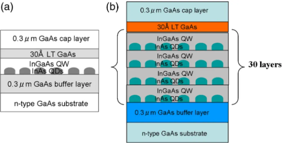
The self-organized InAs QD samples used in this work were grown on n-type (001) GaAs substrates from a solid-source molecular beam epitaxy (MBE). Thefirst set of samples consist of a single layer of InAs QDs with an InGaAs spacer layer in between a 0.3-µm GaAs buffer layer and a 0.3-µm GaAs capping layer was reported previously [3]. The other sample type consists of 30 periods of 2.6 monolayers InAs QDs with 15-nm-thick InGaAs spacer layers bounded by a 0.3-µm GaAs buffer layer and a 0.3-µm GaAs cap-ping layer as shown in Fig. 1. The growth rate for G a A s w a s h e l d b e l o w 1 . 8 6 Å / s . T h e g r o w t h temperature of the QDs and spacer layers was set be-tween 485 and 500°C. The microstructure of samples was investigated by TEM in a JEOL 2010F and STEM was performed in a EM-24015. High-resolution TEM images were obtained along the [111] and [110] di-rections and then converted into FFT images, and high-angle annular dark-field scanning transmission electron microscopy (HAADF-STEM) images were used to determine the dislocation distribution. PL measurements at 300 K were used to characterize the optical properties of the samples. The PL sig-nals were detected using a standard lock-in tech-nique with a continuous-wave 532-nm laser as an excitation source and a near infrared photomulti-plier tube detector. The laser intensity used for ex-citation was 50 mW. RSM of the HR-XRD data was used to determine the strained state of the samples. RSM for the symmetric (004) and asymmetric (224) planes were collected.
Results and discussion
Figure 2 shows PL spectra at 300 K. Two dominant PL peaks from the single-layer QDs appear at 1215 and 1294 nm, their full-width at half-maximum (FWHM) were 51 and 42 nm, respectively. In the case of the multi-layer InAs QDs, two dominant PL peaks at 1145 and 1154 nm with FWHM of 122 and 46 nm were observed. In contrast to the multi-layer InAs QDs, the PL spectra characteristics of the sin-gle-layer InAs QDs suggest that the variety of QDs sizes are responsible for the two peaks detected in Fig. 2. One of the PL peaks observed for the multi-layer InAs QD samples is attributed to the vertically aligned QDs and the other peak originates from the rest of unaligned QDs. The PL results correspond nicely with the STEM images, as shown in Fig. 3.
For the single-layer InAs QDs, a high angle (80 mrad) was used to acquire HAADF images in
Fig. 1.Schematic diagram of the QD heterostructure (a) single-layer InAs QD and (b) multi-layer InAs QDs. Two samples used in this work were grown on n-type (001) GaAs substrates from a solid-source MBE.
900 1000 1100 1200 1300 1400 1x100 2x100 300K-50mW intensity(a.u.) wavelength(nm) Multi-layer InAs QDs Single-layer InAs QDs
Fig. 2.PL spectrum at 300 K of the single-layer InAs QD and the multi-layer InAs QDs.
S150 J O U R N A L O F E L E C T R O N M I C R O S C O P Y, Vol. 59, Supplement, 2010
at National Chiao Tung University Library on April 24, 2014
http://jmicro.oxfordjournals.org/
order to avoid the strain effect interference on the real shape of the QD image. Therefore, the images shown in Fig. 3a and b represent the true size and shape of the single-layer QDs. The QD shape appears to be oval. Based on the STEM images shown in Fig. 3c and d, the multi-layer InAs QDs were aligned vertically along the growth direction and the vertical alignment was dependent on thefirst-layer QD posi-tions. Three different structure types could be ob-served in the sample. First, one column moved toward the other to form one merged column, as shown in Fig. 3c marked A. Secondly, two columns grew closer and then joined to form a wider column, as shown in Fig. 3c marked C. Lastly, one QD stacked on the other to form a perfect vertical align-ment, as shown in Fig. 3c marked B, the QD lateral size was found to increase along the growth direc-tion gradually. Nevertheless, all QDs primarily had a disc-shaped shape. This situation was found to be the same in the InGaAs/GaAs QD system [8]. FFT analysis of the aligned multi-layer InAs QDs in the [110] direction, as shown in Fig. 4d and f, revealed
Moiré fringes pattern indicative of many dislocations in the sample. A careful analysis showed that the upper layer of InAs QDs in the array became shorter in height andflatter than the lower layer of InAs QDs due to strain relaxation by the spacer layer. In com-parison, FFT analysis of the single-layer InAs QDs along the [100] direction only showed a small num-ber of dislocations in the structure, illustrated in Fig. 4b as previously reported [3]. So, we presume that the spacer layers could help to release the strain and cause the QDs to not grow as quickly. The QDs shape, as determined in the HAADF-STEM images, gave an average size of multi-layers InAs QDs of 32 nm in width and 8 nm in height, while the average size of a single-layer InAs QD was 27 nm in width and 11 nm in height. Therefore, the multi-layer InAs QDs are larger in lateral size but shorter in height and flatter than the single layer, which leads to a shorter emission wavelength. This implies that the spacer layers allow strain relaxation leading to QDs that grow in height slowly and cause the multi-layer QDs’s PL emission wavelength to become shorter.
Fig. 3.(a and c) Cross-section bright-field STEM and (b and d) HAADF-STEM images of the single-layer InAs QD and multi-layer InAs QDs on (001) GaAs.
at National Chiao Tung University Library on April 24, 2014
Fig. 4.High-resolution TEM images and FFT analysis of QDs for (a and b) the single-layer InAs QD and (c–f) the multi-layer InAs QD (dot line of the inset box represent the observation area from a vertical QDs arrays).
S152 J O U R N A L O F E L E C T R O N M I C R O S C O P Y, Vol. 59, Supplement, 2010
at National Chiao Tung University Library on April 24, 2014
http://jmicro.oxfordjournals.org/
RSM was carried out as well to provide additional evidence of the strain relaxation phenomenon. The result of the RSM image in symmetric (004) and asymmetric reflection (224) from the HR-XRD meas-urement obtained is shown in Fig. 5. Observation of (004) RSM image is shown in Fig. 5a and b. Observa-tion of (224) RSM image is shown in Fig. 5c and d. Analysis of these images can provide the strain states of the two samples types. The single-layer InAs QD in (224) revealed the full strain because the satellite peak was perpendicular to in-plan com-ponent Qx, as shown in Fig. 5c. As for the multi-layer InAs QDs, the satellite peak represented strain relax-ation, as shown in Fig. 5d. It could assume that the compressive strain in each InAs QD layer was com-pensated by introducing tensile strain by InGaAs
strain-compensating spacer layer. The phenomenon is in agreement with the TEM and the PL results. It could emphasize that dislocation modify the QDs size and optical property because of strain relaxation. It alsofinds out that spacer layers could modify the lat-tice mismatch of the InAs/GaAs system. However, too many spacer layers would lead QDs height to grow slowly to gain shorter emission wavelength. If we could control the appropriate spacer layers, the QDs emission wavelength could be adjusted for op-ticalfibre communication applications.
Summary and conclusion
The single-layer and multi-layer InAs QDs were man-ufactured by MBE. The structural and optical quality
Fig. 5.Reciprocal space maps in (004) reflection of (a) single-layer InAs QD and (b) multi-layer InAs QDs. Reciprocal space maps in (224) reflection of (c) single-layer InAs QD and (d) multi-layer InAs QDs.
at National Chiao Tung University Library on April 24, 2014
and state of strain were assessed by FFT images, HAADF-STEM images and PL and RSM experiments. The presentation of the 15-nm spacer layers in the multi-layer structure modifies the strain around the embedded QDs, which is based on the Moiré fringes pattern of FFT images. The single-layer InAs QDs as a reference take the strain with fewer dislocations. Consequently, the multi-layer InAs QDs average size was shorter in height andflatter than the single-layer InAs QD and caused a decrease in the excited wave-length. RSM images showed the single-layer InAs QD. The result of the RSM image in symmetric (004) and asymmetric reflection (224) corresponds with the FFT images result. Hence, the strains of the InAs QDs are significantly affected by spacer layers, and InAs QDs structural and optical properties depend on strain relaxation. The present observation can help to improve the size and order in multiple-layer InAs/ GaAs QDs array to achieve the promising wavelength for opticalfibre communication systems.
Acknowledgements
The authors are grateful to Mr Chen-Hao Chiang and Dr Jenn-Fang Chen from Industrial Technology Research Institute and Department of Elec-trophysics, National Chiao Tung University for their technical support. The authors are also grateful to Dr Steven Kooi at the Institute for Solider Nanotechnologies, Massachusetts Institute of Technology for his advice.
References
. . . .
1 Arakawa Y and Sakaki H (1982) Multidimensional quantum well laser and temperature dependence of its threshold current. Appl. Phys. Lett. 40: 939.
. . . .
2 Gerald J M, Genin J B, Lefebvre J, Moison J M, Lebauche N, and Barthe F (1995) Optical investigation of the self-organized growth of InAs/GaAs quantum boxes. J. Cryst. Growth 150: 351–356.
. . . .
3 Hsu C C, Hsu R Q, Wu Y H, Chi T W, Chiang C H, Chen J F, and Chang M N (2008) Analysis of InAsN quantum dots by transmission electron microscopy and photoluminescence. Ultramicroscopy 108: 1495–1499.
. . . .
4 Tersoff J, Teichert C, and Lagally M G (1996) Self-organization in growth of quantum dot superlattices. Phys. Rev. Lett. 76: 1675–1678.
. . . .
5 Teichert C, Lagally M G, Peticolas L J, Bean J C, and Tersoff J (1996) Stress-induced self-organization of nanoscale structures in SiGe/Si multilayerfilms. Phys. Rev. B 53: 16334–16337.
. . . .
6 Solomon G S, Trezza J A, Marshall A F, and Harris J S Jr (1996) Ver-tically aligned and electronically coupled growth induced InAs is-lands in GaAs. Phys. Rev. Lett. 76: 952–955.
. . . .
7 Springholz G, Holy V, Pinczolits M, and Bauer G (1998) Self-organized growth of three-dimensional quantum-dot crystals with fcc-like stacking and a tunable lattice constant. Science 282: 734–737.
. . . .
8 Zhuang Q, Li H, Pan L, Li J, Kong M, and Lin L (1999) Self-organized of the InAs/GaAs quantum dots superlattice. J. Cryst. Growth 201: 1161–1163.
. . . .
9 Adhikary S, Halder N, Chakrabarti S, Majumdar S, Ray S K, Herrera M, Bonds M, and Browning N D (2010) Investigation of strain in self-assembled multilayer InAs/GaAs quantum dot heterostructures. J. Cryst. Growth 312: 724–729.
. . . .
10 Akaogi T, Tsuda K, Terauchi M, and Tanaka M (2004) Lattice param-eter dparam-etermination of a strained area of an InAs layer on a GaAs sub-strate using CBED. J. Electron Microsc. 53: 11–19.
S154 J O U R N A L O F E L E C T R O N M I C R O S C O P Y, Vol. 59, Supplement, 2010
at National Chiao Tung University Library on April 24, 2014
http://jmicro.oxfordjournals.org/