Properties of thin Ta–N films reactively sputtered on CurSiO rSi
2substrates
Jui-Chang Chuang
), Mao-Chieh Chen
Department of Electronics Engineering and the Institute of Electronics, National Chiao-Tung UniÕersity, 1001 Ta Hsueh Road, Hsinchu, 300, Taiwan
Received 29 July 1997; accepted 23 October 1997
Abstract
˚
This work studied the thin film properties of 200 A Ta and Ta–N films reactively sputtered on the CurSiO rSi substrates. The2 nitrogen atomic concentration in the Ta–N film was found to saturate at about 30%. Excessive sputtering gas flow, especially the N gas,2 caused surface damage to the sputter deposited films. Thermal annealing in N ambient at temperatures up to 7008C did not change the2 atomic concentrations and the chemical states of Ta and N in the Ta and Ta–N films. The thermal annealing resulted in the grain growth and the healing of sputter damage, but it also induced new defects in the Ta–N films due to thermal stress. This presents a reliability problem in process application involving high temperature thermal cycle. q 1998 Elsevier Science S.A. All rights reserved.
Keywords: Thin film properties; Ta–N; CurSiO rSi2
1. Introduction
Ž . Ž .
Tantalum Ta and Tantalum nitrides Ta–N have been
Ž .
used as diffusion barriers in copper Cu metallization
against interaction between Cu and the underlying
sub-w x
strates 1–5 , and they have been recognized as excellent barriers for the prevention of Cu-diffusion. The damascene
Ž .
scheme of Cu chemical–mechanical polishing CMP
pro-w x
cess uses Ta liners to passivate the interlaced Cu layers 6 . Ta and Ta–N are attractive in many applications because of their good electrical conductivity, high melting point,
w x
and chemical inertness 7–9 . They belong to the class of
w x
dense interstitial compound 2 and are expected to be low reactive with Cu. Many methods have been reported for the deposition of Ta and Ta–N films, for example, reactive
w x Ž .
sputtering 2–5,10 , ion beam assisted deposition IBAD
w11 , and E-beam evaporation 12–15 of Ta–N on siliconx w x w2–5,10–15 , carbon 10 , stainless steel 11 , and silicidex w x w x w13,14 substrates. In this work, we investigated the thinx
˚
film properties of 200 A Ta and Ta–N films reactively sputtered on Cu substrate. This is the beginning phase of study for the passivation capability of Ta and Ta–N films
)
Corresponding author.
against Cu oxidation in the TarCurSiO rSi and Ta–2
NrCurSiO rSi structures.2
2. Experimental details
The substrates used for the deposition of Ta and Ta–N films were p-type, boron-doped Si wafers with nominal resistivity of 17–55 V cm. After initial RCA cleaning, the Si wafers were thermally oxidized at 10508C in steam
˚
˚
atmosphere to grow a 5000 A SiO . A Cu film of 2000 A2
thickness was sputter deposited on the oxide layer. This
˚
was followed by a 200 A Ta or Ta–N film deposition on the Cu layer. The Ta film was sputter deposited using a pure Ta target in Ar ambient, while the Ta–N films were deposited by reactive sputtering using the same Ta target in a gas mixture of Ar and N with various flow rates. The2
base pressure of the sputtering chamber was 5 = 10y7
Torr, and films were sputtered at a pressure of 7.8 mTorr. Table 1 summarizes the sputtering conditions for the Ta and Ta–N films. After the film deposition, wafers were diced into 1.5 = 1.5 cm2 pieces for further treatment. The
diced samples were thermally annealed in flowing N for2 30 min at a temperature ranging from 100 to 7008C. Electrical measurement and material analysis were used to study the film properties. Sheet resistance was measured
Ž .
using a 4-point probe. Scanning electron microscope SEM 0040-6090r98r$19.00 q 1998 Elsevier Science S.A. All rights reserved.
Ž . PII S 0 0 4 0 - 6 0 9 0 9 7 0 0 9 1 4 - 0
Table 1
Sputtering conditions for Ta and Ta–N films
Sample identification A B C D E
Ž . Ž . Ž . Ž . Ž . Ž .
ArrN flow rates sccm2 12r0 58.5r1.5 12r3 12r5 12r12
Ž .
Volume fraction of N in sputtering gas %2 0 2.5 20 29 50
˚
Ž .
Deposition rate Ars 0.3 0.45 0.3 0.3 0.17
was used to investigate surface morphology. Auger
elec-Ž .
tron spectroscopy AES was used for depth profile
analy-Ž .
sis. X-ray photoelectron spectroscopy XPS was used for chemical states analysis.
3. Results and discussion
Ž .
Fig. 1 shows the atomic concentrations at.% of nitro-gen in the sputter deposited films vs. N volume fraction2
in the sputtering gas, as determined from the AES analysis. No nitrogen was detected for samples A and B. The nitrogen at.% was found to be 23.5% for sample C, and increased to 30.5% for sample D. However, no further increase of nitrogen at.% was found for sample E, which
was deposited in an ArrN gas mixture with 50% volume2
fraction of N . The nitrogen at.% in Ta–N saturated at2
about 30%. The chemical states of tantalum and nitrogen in these films were determined using XPS under Mg–K a
Ž . Ž
X-ray irradiation by taking C1s 285 eV and Cu 2p 932.7
.
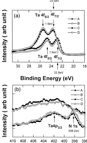
eV as energy references. Fig. 2 shows the binding energy spectra of Ta 4f7r2 and N1s photoelectrons. For sample A and sample B, the binding energy of Ta 4f7r2 photoelec-trons was determined to be 22.8 eV, while no nitrogen signal was found. For the N-doped sample C and sample D, the binding energy of Ta 4f7r2 photoelectrons shifted to 23.5 eV, and N1s signal was found at 398.2 eV. The binding energies of Ta 4f7r2 photoelectrons of
stoichio-w x
metric bcc Ta and fcc Ta–N compounds are 21.9 16 and
w x
22.6 11 eV, respectively. It was reported that the Ta film sputter deposited in Ar ambient belonged to tetragonal Ta, while the reactively sputtered Ta–N film belonged to
Ž .
Fig. 1. Atomic concentrations at.% of nitrogen in sputter deposited Ta and Ta–N films vs. N volume fraction in the sputtering gas.2
Ž . Ž .
Fig. 2. XPS spectra of a Ta 4f7r 2and b N1s photoelectrons for the Ta
Ž .
and Ta–N films samples A, B, C, and D .
Fig. 3. Resistivity of the as-deposited Ta and Ta–N films vs. N volume2
Ž .
fraction in the sputtering gas mixture ArrN . The gas flow rates2 ŽArrN , in unit of sccm are indicated for each sample.2 .
w x
either hexagonal TaN or hexagonal Ta N structure 17 .2
The discrepancy in binding energies of the Ta 4f7r2 photo-electrons is presumably due to structure difference.
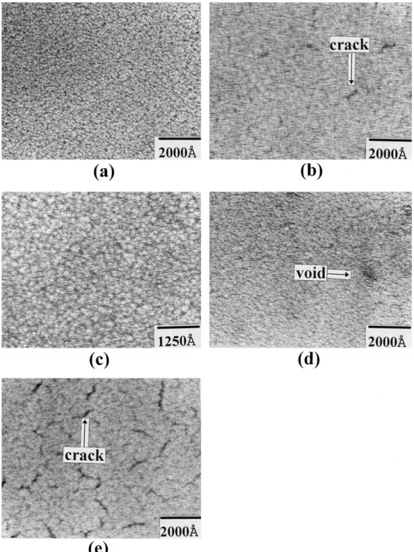
The resistivity and the surface morphology of the as-de-posited films are shown in Figs. 3 and 4, respectively. It can be seen that the film resistivity, surface morphology, and sputtering gas mixture are closely related. Comparison
between samples A and B shows that high Ar flow rate in the sputtering gas resulted in higher sputtering rate and
Ž .
cracked surface Fig. 4b ; thus sample B is slightly more resistive than sample A. Samples C and D were deposited
in ArrN gas mixture with the same flow rate of Ar but2
different flow rate of N . They had the same sputtering2
rate, but the higher N2 content in the sputtering gas
Ž . Ž . Ž . Ž .
Fig. 4. SEM micrographs showing surface morphology of the as-deposited Ta and Ta–N films: a sample A, b sample B, c sample C, d sample D,
Ž .
Fig. 5. Sheet resistance change vs. N annealing temperature for sample2 C.
Ž .
resulted in voided surface Fig. 4d and higher resistivity of sample D. As the N volume fraction increased further2
for the deposition of sample E, the sputtering rate dramati-cally reduced and the surface became seriously damaged
ŽFig. 4e ; thus, sample E has a much higher resistivity..
In the sputtering process, sputter deposition and sputter
w x
etching occur simultaneously 18 . Both energetic Ar and N plasma contributed to the sputter deposition and to the2
sputter etching. By keeping the same deposition pressure, i.e., 7.8 mTorr, for all the samples deposited, we assume that large Ar flow caused surface damage of sample B
ŽFig. 4b . Nitrogen in the sputtering gas mixture not only.
introduced nitrogen into Ta films but also caused excessive energetic nitrogen particles to impinge upon the deposited
Ta–N surface. With more than 30% volume fraction of N2
Ž .
in the sputtering gas sample E , sputter etching took
predominance, resulting in decrease of Ta–N deposition rate and saturation of nitrogen at.% in the deposited Ta–N
Ž .
films Fig. 1 . The similar trend in the saturation of
w x
nitrogen content was reported 10 . We assume that the sputter etching due to excessive energetic N plasma in the2
sputtering gas mixture was responsible for the nitrogen at.% saturation in the deposited Ta–N films. In addition,
the impinging energetic N2 plasma also caused surface
damage as shown in Fig. 4e.
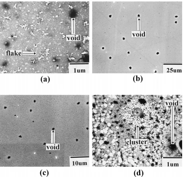
Ž .
Fig. 6. SEM micrographs showing surface morphology of Ta and Ta–N films for the samples thermally annealed at 7008C in N ambient: a sample A,2 Ž .b sample C, c sample D, and d sample E.Ž . Ž .
Fig. 5 shows the sheet resistance change vs. annealing temperature for the thermally N annealed sample C. The2
similar trend showing decreasing sheet resistance with increasing annealing temperature was obtained for the other samples. The reduction of sheet resistance was pre-sumably due to grain growth and sputter damage healing of the Ta–N film by thermal annealing. Fig. 6 shows the surface morphology of Ta–N films after the Ta– NrCurSiO rSi structure was thermally annealed at 7008C2 in N ambient. Compared to the as-deposited films shown2
in Fig. 4, new defects were found on the surface of the thermally annealed samples; these include voids for all thermally stressed samples, flaking due to agglomeration
Ž .
of Ta grains for sample A Fig. 6a , and cluster observed
Ž .
on sample E Fig. 6d . Surface morphology of sample B looks the same as that of sample A. Film stress may be created because of accommodating of thin Ta or Ta–N film’s surface tension during the thermal heating and cooling contours and the difference of grain growth rates
w x
between the films and the underlying Cu layers 18 . To relieve this thermal stress, voids were formed, as shown in Fig. 6. The cluster on sample E was presumed to be a kind of copper oxide cluster, because there was residual oxygen in the annealing ambient and the surface of the
as-de-Ž .
posited sample E was seriously damaged Fig. 4e . The thermal annealing did not result in detectable change of nitrogen at.% in the Ta–N films and chemical states of Ta and N in the Ta and Ta–N films. The binding energies of the Ta 4f7r2 and N1s photoelectrons remained the same as those shown in Fig. 2. Moreover, the elemental depth profiles for the 7008C annealed sample C and sample D, as determined by AES and XPS analysis, showed negligible change as compared to those of the as-deposited sample C and sample D, respectively. This implies that there was negligible interaction between Cu and Ta as well as Cu and Ta–N. Nevertheless, the thermal stress degraded sur-face morphology of the Ta and Ta–N layers.
4. Conclusions
Sputtered Ta and reactively sputtered Ta–N films
de-posited on CurSiO rSi substrates were studied. High2
flow rate of Ar sputtering gas led to faster sputtering rate as well as cracked Ta films. Moreover, high flow rate of
N2 in the sputtering gas mixture introduced excessive
energetic N plasma, resulting in reduced deposition rate2
as well as damaged and higher resistive Ta–N films. The nitrogen atomic concentration in the Ta–N film saturated at about 30%. We assume that the saturation of nitrogen at.% in the Ta–N film is a consequence of sputter etching due to excessive energetic N plasma. The nitrogen at.%2
and the chemical states of Ta and N for all samples did not change after thermal annealing at temperatures up to 7008C
in N2 ambient. Thermal annealing of the Ta –
NrCurSiO rSi structures resulted in reduced sheet resis-2
tance due to grain growth and sputter damage healing of the films; however, new defects were created due to the thermal stress, presenting a reliability problem in process application.
Acknowledgements
The authors wish to thank the Semiconductor Research Center of National Chiao-Tung University and the Na-tional Nano Device Laboratory for providing excellent processing environment. This work was supported by the National Science Council, ROC, under Contract No. NSC-86-2215-E-009-040.
References
w x1 S.Q. Wang, S. Suthar, C. Hoeflich, B.J. Burrow, J. Appl. Phys. 73 Ž . Ž5 1993 2301..
w x2 K. Holloway, P.M. Fryer, C. Cabral Jr., J.M.E. Harper, P.J. Bailey, Ž . Ž .
K.H. Kelleher, J. Appl. Phys. 71 11 1992 5433.
w x3 T. Nakano, H. Ono, T. Ohta, T. Oku, M. Murakami, in: Proceeding
of 1994 VMIC Conference, 1994, p. 407.
w x4 M. Stavrev, C. Wenzel, A. Moller, K. Drescher, Appl. Surf. Sci. 91¨ Ž1995 257..
w x5 B. Mehrotra, J. Stimmell, J. Vac. Sci. Technol. B5 6Ž . Ž1987 1736.. w x6 C.-K. Hu, B. Luther, F.B. Kaufman, J. Hummel, C. Uzoh, D.J.
Ž .
Pearson, Thin Solid Films 262 1995 84.
w x7 D.R. Lide Ed. , CRC Handbook of Chemistry and Physics, 73rdŽ .
edn., CRC Press, Boca Raton, 1992.
w x8 E.A. Brandes Ed. , Smithells Metals Handbook, 6th edn., Butter-Ž .
worths, Borough Green, Sevenoaks, England, 1983.
w x9 T.B. Massalski Ed. , Binary Phase Diagram, 2nd edn., ASM Inter-Ž .
national, Material Park, OH, 1990.
w10 X. Sun, E. Kolawa, J.-S. Chen, J.S. Reid, M.-A. Nicolet, Thin Solidx Ž .
Films 236 1993 347.
w11 K. Baba, R. Hatada, Surf. Coat. Technol. 84 1996 429.x Ž .
w12 L.A. Clevenger, N.A. Bojarczuk, K. Holloway, J.M.E. Harper, C.x Ž .
Cabral Jr., R.G. Schad, F. Cardone, L. Stolt, J. Appl. Phys. 73 1
Ž1993 300..
w13 C.-A. Chang, J. Appl. Phys. 67 12x Ž . Ž1990 7348.. w14 C.-A. Chang, J. Vac. Sci. Technol. A8 5x Ž . Ž1990 3796..
w15 W. Ensinger, M. Kiuchi, M. Satou, J. Appl. Phys. 77 12x Ž . Ž1995.
6630.
w16 C.D. Wagner, W.M. Riggs, L.E. Davis, J.F. Moulder, in: G.E.x Ž .
Muilenberg Ed. , Handbook of X-ray Photoelectron Spectroscopy, Perkin-Elmer, Physical Electronics Division, Eden Prairie, MN, 1979.
w17 D.D. Wu, Master Thesis, National Chiao-Tung University, Taiwan,x
1996.
w18 S.P. Murarka, in: S.M. Sze Ed. , VLSI Technology, 2nd edn.,x Ž .