QPSK Modulation for AC-Power-Signal-Biased Visible Light
Communication System
Yu-Feng Liu
a, Chien-Hung Yeh
b,c, Chi-Wai Chow
a, and Yang Liu
da
Department of Photonics and Institute of Electro-Optical Engineering, National Chiao Tung
University, Hsinchu 30010, Taiwan
b
Information and Communications Research Laboratories, Industrial Technology Research Institute
(ITRI), Hsinchu 31040, Taiwan
c
Graduate Institute of Applied Science and Engineering, Fu Jen Catholic University, New Taipei
24205, Taiwan
d
Hong Kong Productivity Council (HKPC), Hong Kong
ABSTRACT
With the integration of light emitting diode (LED), visible light communication (VLC) can provide wireless communication link using the lightning system. Due to the consideration of power efficiency, AC-LED has the design of reducing energy waste with alternating current from the power outlet. In this work, we propose an power-signal-biased system that provides communication on both DC-LED and LED. The bias circuit is designed to combine AC-power signal and the message signal with QPSK format. This driving scheme needs no AC-to-DC converters and it is suitable for driving AC LED. Synchronization is completed to avoid threshold effect of LED.
Keywords: Wireless, Visible Light Communication, Light emitting diode (LED), AC-LED, QPSK
1. INTRODUCTION
Optical wireless (OW) communications (including visible light and infrared) are attractive access technologies for the next generation (4G) wireless communication system1. For high speed indoor communication, “Visible Light
Communication” (VLC) is a good choice since it can be integrated with lighting infrastructure to provide higher power and a ubiquitous communication system.
Light Emitting Diode (LED) is energy efficient for converting electrical power to light compared with fluorescent and incandescent light. With low-cost, long lifetime, LED is an important role in the lighting applications. With a proper voltage bias and small signal modulation, LED can be modulated with electrical signal to provide visible light communication (VLC) and lightning in the meanwhile.
Compared with radio wave communication, visible light has no electromagnetic interference and thus no license is required. Compared with the infrared (IR), visible light is safer to human eye, and the lightning infrastructure provides large-intensity signal, which can be distributed ubiquitously. Many Research and standardization activities have already been done [1-6], and this topic has been drawing more and more attention. The available bandwidth and spectral efficiency
of VLC can be enhanced by the methods such as orthogonal frequency division multiplexing (OFDM) or discrete multi-tone (DMT) [2-4], pre-distortion, and post-equalization6.
To provide the lightning with large coverage area, the driving circuit designed for LED is an important issue. The electrical power from the outlet is AC power, so it is feasible to use serial connected LED in two directions, which is named AC LED7.
In the previous work on VLC using AC LED, the microcontroller was used to modulate on-off keying signal on AC-powered LED 8,9, and synchronization was made to properly fit the information into the available time slot of the power
signal. Instead of controlling the AC signal with microcontroller, an AC-power-signal biased driving system is proposed with QPSK format to avoid frequency domain overlapping.
WuW
2. EXPERIMENTS AND MEASUREMENT
Fig. 1 shows the experimental setup of AC-power-signal biased driving system. The 110 Vrms AC power is converted to 9 Vrms by transformer. 9 Vrms signal is sent to two paths: clock recovery and full-wave rectifier. The clock recovery circuit generates a square wave with duty cycle close to 50% and the frequency is locked to the AC power signal. The full-wave rectifier flipped the negative-voltage part of the power signal to positive-voltage. Arbitrary waveform generator (AWG, Agilent 33220A, as shown in Fig. 1) generates QPSK format signal with symbol rate of 200 Ksymbol/s and carrier frequency of 400 KHz. The clock recovery circuit provides the AWG the triggering signal for operating in burst mode.
Real-time Oscilloscope
Clock Recovery Circuit
Arbitrary Waveform
Generator
(Agilent 33220A)
Bias Tee Circuit
DC LEDs
Rx
Transformer output
Free space transmission: 2m
Full wave Rectifier
Fig. 1. Experiment setup of the AC-Power-Signal-Biased Driving System
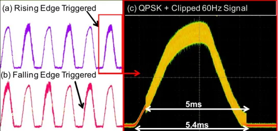
(c) QPSK + Clipped 60Hz Signal (a) Rising Edge Triggered
(b) Falling Edge Triggered
5.4ms 5ms
Fig. 2. Received time domain waveform. (a) Rising edge triggered. (b) Falling edge triggered. (c) Eye-pattern [zooming in part of (a)].
The Bias Tee circuit was designed for combining the AWG output and the rectified AC power; the output of Bias Tee drives a 5×8 LED array, and transmission 2 m distance through the free space.
The LED array in the experiment was a commercial available DC LED array which operates at maximum voltage of 12 V. The PIN receiver (PIN) is used (Thorlabs PDA36A). The gain of the Rx was set to 30 dB to amplify the electrical signal, which was then captured by the real-time oscilloscope (Tektronix DPO 7354C).
To verify the design of clock recovery circuit, the AWG was set to be triggered by rising edge and falling edge, and the result is shown in Fig. 2(a) and Fig. 2(b).The real-time oscilloscope was triggered by the AC line (built-in function), so with different trigger, only half of the 60 Hz cycle can be modulated with message using our equipment. The rising edge setting was used for analyzing the received eye-pattern. The QPSK signal and the rectified 60 Hz signal are clearly added in Fig. 2(c). The half cycle of 60 Hz AC power signal is about 8.33ms. Due to the LED threshold effect, large enough bias is provided only in a time interval of 5.4ms. The burst mode transmit 1000 symbol with a time interval of 5ms. The interval is designed to be within the high-voltage-biased time interval 5.4ms. The experimental result shows that the system successfully transmits a 5 ms QPSK signal within the time slot as can be seen in Fig 2. (c).
3. SUPERPOSITION OF BIAS AND MODULATION SIGNALS
3.1 Transfer function of the system
The bias-tee circuit has two input ports, and one output port. Typically the two inputs have very different frequency; one input is for coupling DC signal (Low-pass), the other for AC signal (high-pass). The message signal with QPSK format has a band-pass spectrum within 200 KHz to 400 KHz. Thus, we put the AC-power a(t) and message signal m(t) into the low-pass end and high-pass end of bias-tee circuit, and the output of the bias-tee circuit is represented as:
) t ( m C ) t ( a C ) t ( x = 1 + 2 (1)
C1 and C2 are constants that determined from the circuit design. This output voltage should exceed the limitation of
threshold voltage of LED to generate a non-distorted optical intensity signal assuming that the V-I curve of LED is linear:
xoptical(t)=C3
(
C1a(t)+C2m(t)−Vthreshld)
(2)In this experiment a(t) varies slow but with large amplitude, so there is only a certain time interval for the equation above to be valid. Otherwise, the signal clipping from threshold voltage will destroy the message signal.
3.2 Signal Spectrum Analysis
By substituting the expression m(t) with a finite duration QPSK format with 2N+1 symbols, the electrical driving signal is:
(
)
∑
− = ⎟ ⎟ ⎠ ⎞ ⎜ ⎜ ⎝ ⎛ − ⋅ + + = N N n symbol symbol n rect T t nT j ft cos C ) t ( a C ) t ( x 1 2 2π φ (3)The Fourier transform at positive frequency range is approximated to be:
⎟ ⎟ ⎠ ⎞ ⎜ ⎜ ⎝ ⎛ − ⋅ ⎟ ⎟ ⎟ ⎠ ⎞ ⎜ ⎜ ⎜ ⎝ ⎛ + = − − = + +
∑
symbol c fnT j N N n j symbol f f f c sin e e T C ) f ( A C ) f ( X symbol n π φ 2 2 1 2 (4)A(f)+ is the positive frequency component of Fourier transform of a(t).
) f f f ( c sin C ) f ( A C ) f ( X symbol c ) Symbols N ( − + = + + + 1 22 1 (5)
The second term contributed from m(t) can be recovered by applying band-pass filter, when this electrical signal is not distorted by threshold voltage effect. In the experiment, fc = 400 KHz, fsymbol = 200 KHz, so the energy of m(t) is highly
concentrated in 200 KHz to 600 KHz in the main lobe of sinc function.
3.3 Compatibility with DC LED and AC-LED
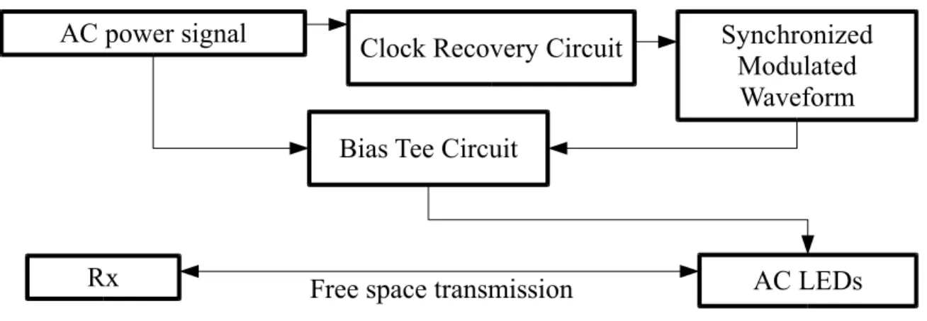
The AC-power-signal-biased driving system is compatible with AC-LED. As shown in Fig. 3, the rectifier is not needed for AC-LED since AC-LED itself supports current in two directions.
Clock Recovery Circuit
Synchronized
Modulated
Waveform
Bias Tee Circuit
AC LEDs
Rx
AC power signal
Free space transmission
Fig. 3. Compatibility of AC-power-signal-biased driving system with AC-LEDs
The clock recovery and bias-tee circuit is unchanged. The similar analysis as in 3.1 and 3.2 can show that the AC-LED system generates non-distorted QPSK in specific time interval. But since alternating polarity of bias signal, the negative cycle of a(t) changes the polarity of the message component of optical signal. It is represented as:
(
threshold)
optical(t) C C a(t) C m(t) V
x = 3 1 + 2 − , for positive linear range (6)
(
threshold)
optical(t) C Ca(t) C m(t) V
x = 3 1 − 2 − , for negative linear range (7)
At transmitter side, the alternating constant of m(t) term can be identified by the clock signal recovered from AC source and eliminated by pre-inversion of logical values in negative linear range. The optical intensity signal is always positive, using the equations of (2), (6) and (7), we can analyze the available time interval for transmitting m(t) linearly for different system design to avoid signal clipping from the threshold voltage of LEDs.
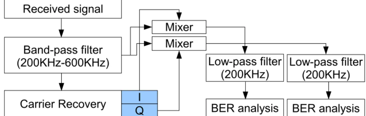
Received signal
Band-pass filter
(200KHz-600KHz)
Carrier Recovery
Mixer
Low-pass filter
(200KHz)
BER analysis
Low-pass filter
(200KHz)
BER analysis
I
Q
Mixer
Fig. 4. The post processing flow: the spectrum of main lobe of sinc function is down-converted.
3.84 3.86 3.88 3.9 3.92 3.94 x 10⁴ -8 -6 -4 -2 0 2 4 6 8 x 10⁻³ 0 2 4 6 8 10 x 104 -0.01 -0.008 -0.006 -0.004 -0.002 0 0.002 0.004 0.006 0.008 0.01 Time (ms) Time (ms) S ig n al A m p lit u d e
Fig. 5. Band-pass filtered signal in time domain: The QPSK signal inside the envelope can be seen.
4. POST PROCESSING OF RECEIVED SIGNAL
The post-processing flow is shown in Fig. 4. With the mathematical description in the above section, we apply the digital band-pass filter (with 200-600 KHz pass-band) to extract the m(t) components of the received signal which is shown in Fig. 2(c). The band-pass filtered signal is shown in Fig. 5. We can see that amplitude fluctuation in Fig. 2(c) is eliminated in Fig. 5(a). By zooming into the Fig. 5(a), we can see that the band-pass filtered waveform has a center frequency of 400 KHz, with 200 Ksymbol/s QPSK modulation as shown in Fig. 5(b). The received QPSK signal is down-converted by mixing a 400 KHz in-phase and quadrature-phase carrier and using low pass filter. The constellation diagram and eye diagram is shown in Fig. 6. The BER of I channel and Q channel is 9.4×10⁻⁵ and 2.1×10⁻⁵; Further
post-equalization can be used to enhance the performance.
-0.5 0 0.5 -5 -4 -3 -2 -1 0 1 2 3 4 5x 10 -3 Time A m pl itude Eye Diagram -0.5 0 0.5 -5 -4 -3 -2 -1 0 1 2 3 4 x 10⁻³ Time A m pl itude Eye Diagram -5 -4 -3 -2 -1 0 1 2 3 4 x 10⁻³ -4 -3 -2 -1 0 1 2 3 4x 10 -3
(a)
(b)
(c)
Fig. 6. Result of signal analysis: (a) Demodulated constellation diagram. (b) Eye-diagram of I channel. (c) Eye-diagram of Q channel.
5. CONCLUSION
The AC-power-signal-biased driving system to provide VLC is experimentally demonstrated. Bias tee circuit was used to combine both the message signal for data transmission and the AC-power signal which provided the large voltage bias for the LED to be operated in the linear region. The message signal was in QPSK format, which is a band-pass signal.
The system transfer function is analyzed with Fourier analysis. The spectral separation is large enough to recover the message without being interfered by power signal. The adaptation of this system to both DC and AC LED is analyzed. The DC LED requires rectifier to transmit on both positive and negative cycles of 60 Hz power, while AC LED itself supports current in two directions and rectifier is needed. Due to the alternating polarity of AC-power, pre-inversion of logical values in negative cycles is needed to transmit m(t) without being disturbed by AC-power. The representation of optical intensity signal is derived to prevent signal clipping.
The effect of LED threshold voltage was observed, so there was a limited portion of time that was capable of transmitting low current message signal. The synchronization was done to correctly align the message signal in time domain.
In the experiment, the message signal dynamically drove the DC 40-LED array. The 200 Kbps symbol rate QPSK signal was successfully transmitted at specific time interval synchronized with full-wave rectified AC-power signal; the bit rate in average is 120 Kbps, which could be doubled either by making the burst signal been triggered by both rising and falling edge or using AC LED without full-wave rectifier. Bit error rate (BER) below 10−4 with a transmission
distance of 2 m is demonstrated. The equalization techniques can also be further used to enhance the system performance. In conclusion, the proposed AC-power-signal-biased driving system is useful for distributing low current message signal to multiple LEDs simultaneously, and the AC-power signal is compatible with AC LED, which is power efficient since the AC-to-DC converter is not needed.
REFERENCES
[1] K.-D. Langer and J. Vučić, “Optical wireless indoor networks: recent implementation efforts,” European Conference on Optical Communication (ECOC), Paper We.6.B.1 (2010).
[2] J. Vučić, C. Kottke, S. Nerreter, K.-D. Langer, and J. W. Walewski, “513 Mbit/s visible light communications link based on DMT-modulation of a white LED,” J. Lightwave Technol., 28(24), 3512-3518 (2010).
[3] H. Elgala, R. Mesleh, and H. Haas, “Indoor broadcasting via white LEDs and OFDM,” IEEE Trans. Consum. Electron., vol. 55, 1127-1134 (2009).
[4] Y. F. Liu, C. H. Yeh, C. W. Chow, and Y. Liu, “Optimized OFDM modulation format for white-light LED optical wireless communication with pre-equalization,” International Conference on Information Photonics & Optical Communications (IPOC) (2011).
[5] C. W. Chow, C. H. Yeh, Y. F. Liu and Y. Liu, “Improved modulation speed of the LED visible light communication system integrated to the main electricity network,” Electron. Lett., vol. 47, 867-868 (2011). [6] H. L. Minh, D. O'Brien, G. Faulkner, L. Zeng, K. Lee, D. Jung, Y. Oh, and E. T. Won, “100-Mb/s NRZ visible
light communications using a postequalized white LED,” IEEE Photon. Technol. Lett., vol. 21, 1063-1065, (2009).
[7] D. Allen, “LED assemblies and light strings containing,” US Patent, 20060007679A1 (2006).
[8] F. L. Jenq, Y. C. Pu, and Z. C. Weng, “An AC LED smart lighting system with white light FSO communication,” Computer Communication Control and Automation (3CA), 488-491 (2010).
[9] F. L. Jenq, Y.-C. Pu, and W.-C. Du, “A smart lighting system with white LED FSO communication,” Proc. Computer Communication Control and Automation (3CA), 492-495 (2010).