Irr V.
esigns for video-signal
T.-S.Chang C.-W.J en
Indexing terms: Video-signal processing, On-chip memory designs
Abstract: Two embedded memory designs are
proposed for video-signal processing. Concurrent line access performs multiple-port memory accesses at the hardware cost and access time of a single port. It uses 62.24% of the area required by a conventional dual-port memory and is only 7.6% larger than a single-port 2 K x 8 memory.
The block-access mode combines address
decoders and generators, yielding block-access mode times 26% faster than conventional schemes for a 256 words x 32 bits memory size. Despite some preferred-access-order restrictions, the designs incur no loss of generality because video algorithms possess high data parallelism and low dependence.
1 Introduction
Bandwidth mismatches between memories and proces- sors have arisen in recent years and are expected to become more problematic in the future [l]. Real-time video processing such as HDTV and multimedia sys- tems requires huge amounts of video data in a limited processing time, worsening the problems. Memory bandwidth is becoming the main bottleneck for high performance processors. Various solutions [2-91 have been proposed. Among them, on-chip memory [5-91 provides a fast easy-to-use way for chip designers to integrate with their logic circuitry. On-chip memories can store data needed for immediate computation and provide data parallelism to relieve the chip IiO burden.
On-chip memory should be high speed and have a small area, to provide sufficient bandwidth for process- ing elements while holding down costs. Previous on- chip memory designs [5, 6, 81 were usually for general purpose applications that do not require any special addressing functions. However, these special addressing
functions can speed up data accesses in video applica- tions. Existing on-chip memory designs in video-signal processing chips [7, 8, 10-141 do not make full use of this capacity, leading to wasted area and bandwidth. 0 IEE, 1997
IEE Proceedings online no. 19971009
Paper first received 30th November 1995 and in revised form 10th June 1996
The authors are with the Department of Electronics Engineering and Institute of Electronics, National Chao Tung University, Hsinchu 30010, Taiwan, Republic of China
Addressing ability can be explored by considering the characteristics of video-processing algorithms.
In this paper, we propose two on-chip memory mod- ule designs [9] to solve the problems above. The designs are based on the data characteristics of video-signal- processing algorithms. We propose the preferred-access ordering for use in video-signal processing. Unlike con- ventional memory that can be accessed at any time and any location, preferred-access ordering places access constraints on read and write time and locations. These constraints are tailored to the memory architecture, and do not entail any loss of freedom in algorithm exe- cution owing to parallelism in video data. We make use of these constraints to construct embedded memory customised for use in video-signal processing. The first design places constraints on read and write time to allow concurrent line accessing. It emulates multiple- port functioning at an area cost comparable to a single- port cell. The second design places constraints on read and write locations, allowing a block-access mode to reduce access time and provide block-addressing facili- ties.
Table 1: Data sequences of some video algorithms
Algorithms Inter-block Intra-block
Motion algorithm-dependent free estimation
DCT free algorithm-dependent
Quantisation free Quantisation-table-
dependent 2 Characteristics of video-processing algorithms
In designing an efficient on-chip memory, we first con- sider the addressing requirements of video-processing algorithms. Table 1 shows the data sequences of these algorithms; where the inter-block sequence is the block- access order and the intra-block sequence is the pixel- accessing order within blocks. The free ordering implies that we can design a memory that is suitable
for
fast accessing, yet is small in area. We can summarise video algorithms’ features as follows:1 Parallelism: Independent processing ordering exists for data in different blocks and different pixels in the same block. This inter-block and intra-block independ- ence let us arrange access ordering freely.
2 Block operation: Video-data-processing algorithms often deal with 8 x 8 or 16 x 16 block units. Block accessing and storage is a good basis for video-signal- processing memory designs.
IEE Proc -Circuats Devices Syst , Vol 144, No 3, J m e 1997
3 Regular and repeatable: Most video data sequences appear in regular row-scans. Video data is used repeat- edly. This simplifies address generation and reduces storage requirements.
4 Data buffering: In many designs, memory acts simply as a buffer, for example, transposed RAM in 2D DCT/ IDCT, and the digital delay line in HDTV [15]. Digital delay lines use synchronous read and write operations. Once data has been read, the same location can then be used for a write operation.
-
-
L a, V 0 U a, -0 3 P unselected cells cellsn
f i l
r
\+
selected cells column decoderport 1 data I/O
Fig. 1 Conventional memory-access architecture
-
L W -0 U a, -0g
port 2 column decoder
4
cells
t
port 1 data I/O Fig. 2 Concurrent line-access architecture
3 Concurrent line access 3.
I
Operation principleIn conventional memory, as shown in Fig. 1, the row decoder strobes one of the word lines, and the column decoder selects one word from this strobed line of cells. Other columns of cells in the same word line are turned off during the access operation. If we add additional
IEE Proc.-Circuits Devices Syst., Vol. 144, No. 3, June 1997
peripheral circuits to turn on the column selections, we can have multiple accesses in the same access cycle. This architecture for multiple accesses in the same memory row is called concurrent line accessing, as shown in Fig. 2. The access constraint on this architec- ture is that all ports must use the same row address to access the cells, which is useful in video-signal process- ing owing to its ‘free-order’ accessing characteristics.
Fig. 2 shows a block diagram of concurrent line accessing that performs two accesses on the same row. The port column decoders are placed at the opposite sides of the memory array. When a word line is selected, column selections for two sides are turned on exclusively. Two reads, two writes, or one read and one write are all acceptable to this architecture. Concurrent line accessing works like a multiport memory except that row addresses are the same. As in a multiport memory, the same address cannot be read and written to simultaneously. Thus no interference exists between read and write data in this architecture. Each cell in the row can be accessed if enough peripheral circuits are provided. If the column selection is M: 1, we can emu- late A4 ports at most in the same access cycle.
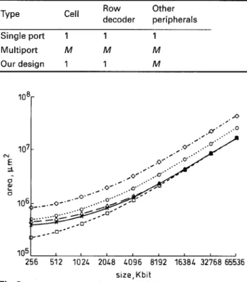
Table 2: Area comparison, assuming port number is M
ROW Other decoder peripherals Single port 1 1 1 Multiport M M M Ourdesign 1 1 M I O 8 [ 1051 1 256 512 1021 2OL8 1096 8192 16381 32768 65536 size,Kbit
Fig.3 Area comparison of one, two and three ports and the authors’
design for two and three ports
All are read-write ports. The area cost of one port and the authors’ two port
design are very close
-X- authors’ two-port design
- -0- - one port
0 two ports
-A- authors’ three-port design
- 0. - three ports
3.2 Performance comparison
The hardware cost of concurrent line accessing is very close to that of a single-port memory and much lower than that of a multiport memory. Table 2 lists an area comparison between this design, single-port and multi- port memories. The advantage of low hardware cost mainly comes from the use of single-port cells. Single- row decoder design also contributes to area reduction. The numbers of other peripheral circuits are the same as in a multiport memory. Fig. 3 shows an area com- parison between one, two and three ports, and our
design for two and three ports with various memory sizes. Our two-port design uses 62.24% of the area required by a conventional two-port memory, and is 7.6% larger than a one-port memory for the 16 Kbit (2K x 8 bit) size, as expressed using the TSMC 0 . 8 ~ SPDM CMOS process, and area reduction increases as the memory size grows.
When this scheme is integrated into a system, the interface used can be identical to a conventional multi- ple-port design. When two ports are used, the system sends two addresses to the memory. One address con- sists of the row address and the column address, and the second address consists of a column address. The second address can also include the row address, but this row address is forced to be the same as the row address of the first address. Thus no additional chip area penalty is incurred by using concurrent line access- ing.
The access time for concurrent line accessing is almost the same as that of a single-port memory. Fig. 4 shows the SPICE simulation result for one to four port designs with the 256 words x 256 bits size. The SPICE simulation was run on a typical TSMC 0.8p-i SPDM technology model, and included parasitic capacitance and resistance. The simulation results show similar delays for different port designs, because we add only an additional column decoder to the bit line loading. The loading of these column decoders has little impact on the overall delay. An additional benefit is that this architecture eliminates the cell instability of conven- tional multiple-port memories, because it uses a simple single-port cell. r I I I I3 2
1
r data input- I - D rc DCT 2 t data seq.l = transposed outRAM
-
I
0 1I
280'
0 282 28L 2 8 6 2 88 290i
time, ns Fig.4top to bottom) under typical conditions one port
-A CLK 1 ---U D1 OUT two, three and four ports
-A DI OUT
SPICE simulation result for one, two, three and four ports ( f o m
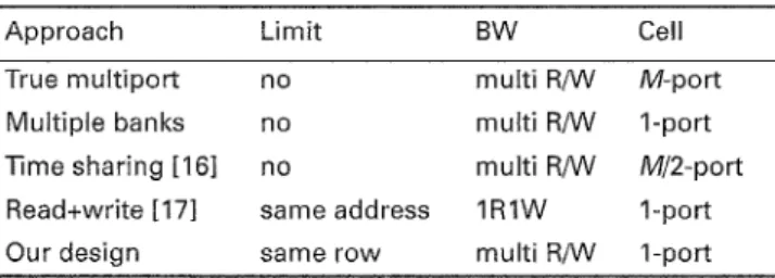
We also made a comparison between different multi- ple-port approaches and our method, as shown in Table 3. True multiple-port memories have larger areas owing to their cells and peripheral circuits. Time-shar- ing [16] and read+write techniques [17] incur longer access-time penalties. Multiple-bank designs implement concurrent access between the memory banks, while our design moves the concurrency into the memory bank to achieve a smaller, more compact construction than multiple-bank designs. Hence, our design applies
access constraints to save the chip area while maintain- ing single-port access time, and is therefore suitable for video-signal processing.
Table 3: Comparison of multiport approaches
Approach Limit BW Cell
True multiport no multi R / W M-port
Multiple banks no multi R / W I - p o r t
Time sharing [I61 no multi R/W M/2-port
Read+write [I71 same address I R I W I - p o r t Our design same row multi R/W I - p o r t
3.3 Design applications
Concurrent line accessing can be applied to the buffer function that is demanded in most video-signal proces- sors. In applications in which the memory acts as a buffer, we can place the read in half of the memory matrix and write accesses in the other half. Fig. 5
shows this data organisation for a l R l W design. Half of the memory columns are for read operations and half of the memory columns are for write operations. Thus we can perform read and write operations simul- taneously using concurrent line accessing. The read and write columns are swapped when no new data exists in the read columns. We have applied this architecture to the transposed RAM design of a two dimensional DCT [18]. The accessing sequence of the 2-D DCT is shown in Fig. 6. In the first x-dimensional DCT, data sequence 1 is written to the memory in row-scanning order. We transpose the sequence by accessing the memory in column-first order, as shown in Fig. 6. Repeating this accessing order, we can access the mem- ory smoothly at a low area cost.
I"
"
.
_..__ ~~
1 : :
ii .
. .'
:
-
._.. .-I
' , i..
. . . . ..., . . : i : ' i.I.:
.i.
...+ . .I ! Fi .5 mr%@iexing = 4 designThe grey and white regions are for different ports
One of the physicul datu organisations for a IRl W and column
seq. 2
a
initial-Y-dim +X-dim--cy-dim --tX-dim-
column row column row
write write write write
column column
read read
seq. 1
seq. 2 data .
inout input input input
data row row
out read read
b
Fig.6
a System block diagram
b Access sequence
Design example for 2 - 0 DCT
Since concurrent line accessing uses the same row addresses for all ports, this architecture features syn- chronous accessing for all ports, useful in line-delay
applications [15]. Fig. 7 shows the block diagram for fixed-delay line. The memory size is the required delay length. The final word of the row uses two-port mem- ory cells. After the memory is filled with data, the read operation begins and starts concurrent line accessing. The last word of the row is written through the second port of the memory cell to avoid data interference, since the read address has been changed to the next row. We connect the word-line selection of the second port to the word-line signal of the next row. The sec- ond port selection for the final word in the final row is connected to the word-line signal of the first row. The address-decoding circuit of the first row is duplicated to avoid an unnecessary propagation delay. This address-decoding circuit can be simply a single NAND gate to connect required addresses, since this delay is for write operations, and is not critical for the concur- rent line-accessing operation.
start address reg. write-input circuit and write-column selection
-
WLO WL1 WL2 WLn-1 WLnt
t
- serial MUX --c distance- adder L end reg. address-
TI
COLnl l ~ n ~ c o L n - ~~COLO
ITLO
read- output circuitread -column selection
address decoder Fig. 7 Design example: circuit diagram offixed delay
A variation of concurrent line accessing combines other multiport techniques with this one. For example, using N-port cells instead of single-port cells increases the bandwidth by N times. We can also pipeline the concurrent line accessing to reduce access time. Since the data flow of read and write operations is not identi- cal, we can use the similar pipeline stages in [16] to ensure the row address is consistent in the cell-array stage for proper pipeline operation.
4 Block-access mode
4.1 Operating principles
Memory accesses in general purpose applications are often random, and have no fixed rules. This can be used for video applications, but is not efficient. Video applications characteristically require block-unit opera- tions and have high parallelism. This implies that we can design an access ordering that satisfies the block- operation requirement and makes full use of parallel- ism. One approach that incurs minimum hardware cost matches the memory architecture for optimum per- formance. The memory architecture is faster when we access the same row of cells, as in page-mode DRAM. Therefore we propose using pixel-serial block-access ordering. This access ordering accesses the whole mem-
IEE Proc-Circuits Devices Syst., Vol. 144, No. 3, June 1997
ory in block units and accesses pixel data within blocks serially. This access ordering is called the block-access mode, and features regular address transitions between two continuous accesses. This mode works for most video-signal processing without loss of algorithm gener- ality because of its high degree of parallelism.
To satisfy the addressing requirements of video appli- cations, the block-access mode performs four functions: row and column scans, forward and backward shifts, programmable shifts and boundary resets. Combina- tions of these functions can generate desired addresses for video applications. The design of this circuit com- bines the address generator and address decoder. The circuitry has two operating modes: default mode and block-access mode. The default mode is normal RAM random access, and the block-access mode accesses blocks of data. In the initial stage, the block-access mode sets parameters of the initial starting address, ending address and block distance, as illustrated in Fig. 8. These parameters define the block-unit access order. start address- current
r
block end -address block distance7
--1 7 I block I I next I r - - - + - - - J next I block I L - - J Fig. 8 Parameters of block-access modetwo - Level
The pixel-access order in blocks is automatically gen- erated by the address generator. Pixel-access ordering uses serial shifts for faster accessing. These serial shifts are performed by shift register chains. However, the block-access mode is different from serial-access mem- ory [19, 201. In this scheme, the start address, end address and shift amount are programmable. The order is not restricted to serial sequence as in serial-access memory.
Fig. 9 shows the block diagram of the circuit design. We first decode the initial address and feed it into the shift-register chain. The end address is then input to determine the end of the block. At the same time, a serial adder adds the block distance to the end address as the start address of the next block. Since most blocks are 8 x 8 or larger, there is enough time to cal- culate the addresses.
4.2 Circuit design
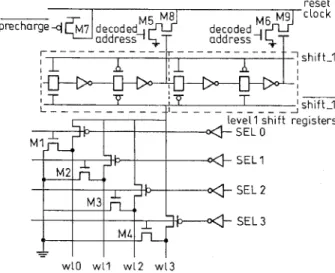
Direct cascading to form shift-register (SR) chains accumulates high capacitance on -the driving clock lines. We propose a two-level SR chain design to gener- ate a local clock for fast shift operation, as shown in Fig. 10. Fig. 11 shows the schematic diagram of the design. A word line is selected by the combination of a level-one and a level-two SR output. We partition the long SR chain into several small clusters. Each cluster has its own local shift-clock signal to avoid high global clock capacitance. In each cluster, multiple word lines share a level-one SR. We use the level-two SR to select the desired word line.
SelO Sell Se12 Se13
~~
Fig. 10 Conceptual diagram of the two-level shift-register chain from previous
address shift-2 clock to next cluster Fig. 11 Schematic diagram of the two-level shift-register chain
In this structure, addresses are shifted by the level- two SR chain until the final location of the chain is reached. The clock and address are then ANDed to generate a local shift-1 signal for the level-one SR chain. Since multiple word lines share one shift register, we have wide pitches to lay out the two-level SR into a one column compact area. The number of AND gates
required to connect the clock signal is C = Wl(R1
*
S). The SR numbers that connect shift-1 and shift-2 sig- nals are R1 and LR2 = WIRI, respectively, where W is the word-line number, R1 is the level one SR number in one cluster, and S is the level two SR number in one cluster. For example, if we set W = 256, R l = 16 and S= 4, we get C = 4, LR2 = 16. The signal loading is reduced considerably compared with the original W =
256 SR loads. A large clock buffer is unnecessary and signal delays are reduced to 0.4ns (for LR2 = 16) and 0.2111s (for C = 4) for the TSMC 0 . 8 ~ SPDM CMOS process as determined by SPICE simulation.
reset
Fig.
wio w l l w12 w13
1 2 Circuit diagram of the shift-register (SR) chains
Fig. 12 shows the circuit design. We add MI-M4 to ensure that unselected word lines are pulled down to the ground at SELO-SEL3 OFF. The serial shift func- tion is performed by continuous shifting. The block- access mode is first initiated by setting the start address, end address and block displacement. These parameters are stored in registers. The start address is first decoded and loaded into the SR chain. Then the end address is decoded and connected to the gates of transistors M8 and M9 to check the shift operation end information. When the data has been shifted to the block end, transistor M5 or M6 is turned on by the data end. The reset clock is discharged through the transistor as M8 or M9. This reset clock pulse starts the loading of a new start address.
4.3 Performance comparison
The current designs of the video-signal processor use an extra address generator to generate desired addresses. Thus the memory-access time is lengthened from address generation to data output. Our design ini- tially operates like an address generator, but we save the address generation and decoding delay. For a coun- ter-based address generator design [21], the delay is 4.6811s for the TSMC 0 . 8 ~ SPDM CMOS process. For a memory size of 256 x 32 bits, the access time is 4.3ns, and the decoding time is 1.511s as determined by SPICE simulation. The access time is 3.411s in our design as determined by SPICE simulation, roughly a 26% improvement. This simulation was conducted on a typical TSMC 0 . 8 ~ SPDM process model, and included parasitic capacitance and resistance. Delays can be further reduced by overlapping shift delay and bit line precharging.
When the block-access mode is integrated into a sys- tem, the additional hardware requirement over that of
a conventional memory design is the shift-register chain and address-calculation circuit. The address-calculation circuit is small compared to the decoder. The height of the shift-register chain is equal to the height of the memory matrix for the compact layout. The width of the shift register chain for the design in Fig. 12 is approximately equal to the width of an 8-bit address decoder. From the system viewpoint, no additional lay- out area is required for other hardware. Overall per- formance can be speeded up compared with a conventional design. The system does not need to use an additional cycle when this design is used.
I
I - D l ~ t r a n s p o s e d l ~ 1-DI
transform R A M transform U I U a initial writewrite row column row column
( s e a l ) order order order order
read column row column
(sea 2 ) order order order b
Fig. 13
tion in orthogonal transform a System block diagram
b Access ordering
Memory-access ordering example for row-column decomposi-
L -
EI
operation diagram
j
3
j
L
s
i
f
$row scan-shift columnsL - - - J L - - - J L - - - A
b Fig. 14
a Full-search block-matching algorithm
b Three-step search algorithm
I I -
Memory-access ordering exumple for motion estimation
4.4 Design applications
The block-access mode can be used by most block- based video algorithms. The simplest one is only linear addressing. This can be done by row-scan ordering. In the orthogonal transforms that use row-column decom- position to compute image data, intermediate data is transposed for different dimensional processing. Fig. 13 shows the read and write sequences. We adopt the con- current line accessing to perform read and write opera- tions simultaneously. Intermediate data can be fully stored in the processing memory and in the same order
IEE Proc.-Circuits Devices Syst., Vol. 144, No. 3, June 1997
as in the read sequence. We simply change the row and column scan ordering alternatively to access the desired transposed sequence.
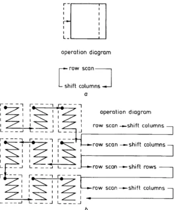
Fig. 14 shows another access example applied to motion estimation. For a full search block-matching algorithm, block operations are overlapped. The access operation performs row-scan ordering for each block and shifts one column for different blocks, as shown in Fig. 14a. For the three-step block-matching algorithm, each step goes through nine locations. The access oper- ations perform row-scan ordering of each block loca- tion. We shift columns for different blocks in the same row and shift rows for different blocks in the same col- umn, as shown in Fig. 14b. All the access operations are in row directions or in column directions. The algo- rithm generality is maintained though the processing order has been rearranged. With some limitation on access locations, we get the benefits of reduced access time and easier addressing.
5 Conclusion
Video-signal processing often requires fast embedded memory to provide a sufficient bandwidth to data path. We have shown that by taking advantage of video-signal processing features we can design applica- tion-specific embedded memory with the potential to reduce area cost and increase speed. We have com- pleted two such designs. The first design applies con- straints on read-write time and can perform multiple accesses of one row within one access cycle. For fixed delay or buffering applications, it emulates multiple- port functioning at single-port cell cost and small access-time overhead. Layout area is 62.24 ‘YO of a two port 2K x 8 implementation. The second design applies constraint on read-write location, and adds shift regis- ters for direct address decoding and generation. In applications using the block-access mode, it maximises the performance by saving address generation and decoding time. SPICE simulation results show a 26% delay improvement. These two designs can be com- bined or used separately.
References
PRINCE, B.: ‘Memory in the fast lane’, ZEEE Spectr., 1994, pp. 38-41
OHSHIMA, S., and FURUYAMA, T.: ‘High speed DRAMS with innovative architectures’. IEICE Trans. Electron., 1994. e l l - C, pp. 1303-1315
TAKAI. Y.. NAGASE. M.. KITAMURA. M., KOSHIKAWA, Y., YOSHIDA, N., KOBAYASHI, Y., OBARA, T., FUKUZO, Y., and WATANABE, H.: ‘250 Mbytekc synchronous DRAM using a 3-stage-pipelined architecture’. Symp. on VLSI Circuits Digest of Technical papers, June 1993, pp. 59-60
YOO, H., PARK, K., CHUNG, C., LEE, S., OH, H., SON, J., PARK, K., KWON, K., HAN, J., MIN, W., and OH, K.: ‘A 150 Mhz 8-Banks 256M synchronous DRAM with wave pipelining methods’. ISSCC Digest of Technical Papers, Feb. 250-251, pp. 1995
SHINOHARA, H., MATSUMOTO, N., FUJIMORI, K., and KATO, S.: ‘A flexible multiport RAM compiler for data path’. IEEE Custom Integrated Circuits Conference, 1990, pp. 16.5.14 SILBURT, A., PHILLIPS, R., GIBSON, G., WOOD, S.,
BLUSCHKE, A., FUJIMOTO, J., KORNACHUK, S.,
NADUEAU-DESTIE, B., VERMA, R., and DIEDRICH,
P.M.J.: ‘A 180-Mhz 0.8-ptn BiCMOS modular memory family of DRAM and multiport SRAM’, ZEEE J. Solid-State Circuits, 1993, 28, pp. 222-232
WILLIAMS, T., BILODEAU, L., BURROUGHS, S.,
FURST, R., POKORNY, W., and SCHROER, G.: ‘A 200-Mhx 8Kb SRAM macro for video applications’. IEEE Custom Inte- grated Circuits Conference, 1993, pp. 25.6.1-3
MIZUKAMI, M., SATOH, Y., KOZAKI, T., and MIKAMI, Y.: ‘CMOS embedded RAMS for digital communication systems’, IEICE Trans. Electron., 1994, E77-C, pp. 1361-1368
9 CHANG, T.S., and JEN, C.W.: ‘Embedded memory module design for video signal processing’. IEEE VLSI signal processing 10 MINAMI, T., KASAI, R., YAMAUCHI, H., TASHIRO, Y., TAKAHASHI, J., and DATE, S.: ‘A 300-Mops video signal processor with a parallel architecture’, IEEE J. Solid-State Cir- cuits, 1991, 26, pp. 1868-1875
11 GOTO, J., ANDO, K., INOUE, T., YAMASHINA, M., YAMADA, H., and ENOMOTO, T.: ‘250-Mhz BiCMOS super- high-speed video signal processor (S-VSP) ULSI’, IEEE J. Solid- State Circuits, 1991, 26, pp. 1876-1883
12 INOUE. T.. GOTO. J.. YAMASHINA. M.. SUZUKI. K.. VIII, Oct. 1995, pp. 801-510
NOMURA, M , KOSEKI, Y , HAMATAKE, N , KUMAA-
GAI, K , ENOMOTO, T , YAMADA, H , and TADAKA, M ‘A 300 Mhz 16bit BiCMOS video signal processor’ ISSCC Digest of Technical Papers, 1993, pp. 37-38 and 258
13 AONO, K., TOYOKURA, M., ARAKI, T., OHTANI, A., KODAMA, H., and OKAMOTO, K.: ‘A video digital signal processor with a vector-pipelined architecture’, IEEE J. Solid- State Circuits, 1992, 27, pp. 1886-1894
14 VEENDRICK, H., POPP, O., POSTUMA, G., and LECOU- TERE, M.: ‘A 1.5 GIPS video signal processor (VSP)’. IEEE Custom Integrated Circuits Conference, 1994, pp. 6.2.14
15 MATSUMURA, T., YOSHIMOTO, M., MAEDA, A., and HORIBA, Y.: ‘A high-performance reconfigurable line memory macrocell for video signal processing ASICS’, IEICE Trans.,
1991, E 7 4 , pp. 3787-3795
16 ENDO, K., MATSUMURA, T., and YAMADA, J.: ‘Pipelined, time-sharing access technique for an integrated multiport mem- ory’, IEEE J. Solid-State Circuits, 1991, 26, pp. 549-554
17 DICKINSON, A., NICOL, C., RAO, S., and HATAMIAN, M.: ‘Application specific memories for ATM packet switching’. Inter- national Symposium on Circuits and systems, 1994, pp. 3.169-172 18 CHEN, C.: ‘Design and implemtation of discrete cosine trans-
form’. Master’s thesis, National Chiao-Tung University, 1995 19 FENSTERMAKER, L.R., and O’CONNER, K.J.: ‘A lower-
power generator-based FIFO using ring pointers and current mode sensing’. ISSCC Digest of Technical Papers, 1993, pp. 242- 243
20 SCHULTZ, K.J.: ‘A modular memory and process verification vehicle for a sub-micron BiCMOS telecom technology’. IEEE Custom Integrated Circuits Conference, 1991, pp. 18.6.14 21 WANG, 3.: ‘Data sequencer design for video processing’.