Pentacene-based thin-film transistors with multiwalled carbon nanotube source and
drain electrodes
Chia-Hao Chang, Chao-Hsin Chien, and Jung-Yen Yang
Citation: Applied Physics Letters 91, 083502 (2007); doi: 10.1063/1.2771532
View online: http://dx.doi.org/10.1063/1.2771532
View Table of Contents: http://scitation.aip.org/content/aip/journal/apl/91/8?ver=pdfcov Published by the AIP Publishing
Articles you may be interested in
Performance improvement in transparent organic thin-film transistors with indium tin oxide/fullerene source/drain contact
Appl. Phys. Lett. 95, 163303 (2009); 10.1063/1.3240893
Poly( 3 , 3 -didodecylquarterthiophene) field effect transistors with single-walled carbon nanotube based source and drain electrodes
Appl. Phys. Lett. 91, 223512 (2007); 10.1063/1.2806234
Transparent flexible organic thin-film transistors that use printed single-walled carbon nanotube electrodes Appl. Phys. Lett. 88, 113511 (2006); 10.1063/1.2181190
Pentacene-carbon nanotubes: Semiconducting assemblies for thin-film transistor applications Appl. Phys. Lett. 87, 203510 (2005); 10.1063/1.2132063
Organic Thin Film Transistor with Carbon Nanotube Electrodes AIP Conf. Proc. 786, 508 (2005); 10.1063/1.2103919
This article is copyrighted as indicated in the article. Reuse of AIP content is subject to the terms at: http://scitation.aip.org/termsconditions. Downloaded to IP: 140.113.38.11 On: Wed, 30 Apr 2014 07:02:17
Pentacene-based thin-film transistors with multiwalled carbon nanotube
source and drain electrodes
Chia-Hao Chang
Department of Electronics Engineering, National Chiao Tung University, Hsinchu, Taiwan 300, Republic of China
Chao-Hsin Chiena兲
Department of Electronics Engineering and Institute of Electronics, National Chiao Tung University, Hsinchu, Taiwan 300, Republic of China
Jung-Yen Yang
National Nano Device Laboratories, Hsinchu, Taiwan, Republic of China
共Received 9 May 2007; accepted 24 July 2007; published online 20 August 2007兲
In this letter, the authors propose a practical and reliable approach—using deposited multiwalled carbon nanotubes共MWCNTs兲 as source and drain electrodes—for reducing the contact resistance 共Rc兲 in pentacene-based bottom-contact thin-film transistors. The value of Rcof the devices was
closely linked to the resultant length of the deposited MWCNTs; the lowest value was 3 ⫻108⍀m. The largest saturation mobility was 0.14 cm2/ V s; this value reached up to three times
higher when the threshold voltage was determined using the maximum transconductance共Gm,max兲
extrapolation method, rather than the constant current method. The on/off ratio was more than 106. © 2007 American Institute of Physics.关DOI:10.1063/1.2771532兴
Pentacene-based organic thin-film transistors 共OTFTs兲 have been attracting much attention because of their rela-tively low cost and the feasibility of fabricating them on flexible organic substrates at low temperature. Currently, two typical device structures are employed for the fabrication of OTFTs, i.e., bottom-contact OTFT 共BC-OTFT兲 and top-contact OTFT-共TC-OTFT兲. When pursuing denser electrical circuits, BC-OTFTs have an advantage over TC-OTFTs be-cause exposure of the active organic material to solvents and chemicals can be avoided during the lithography process.1 Nevertheless, the performance of BC-OTFTs is usually infe-rior to that of TC-OTFTs because of higher contact resistance 共Rc兲 at the source/drain 共S/D兲 electrodes; this phenomenon
has been investigated extensively.2,3 Carbon nanotubes 共CNTs兲 have been the focus of much recent research because of their unique electronic properties and extraordinary me-chanical properties.4,5 Single-walled carbon nanotubes 共SWCNTs兲 have been demonstrated as highly useful materi-als in nanoscale devices, while multiwalled carbon nano-tubes共MWCNTs兲 have great potential for the field emission applications and as interconnects.6–8
In this letter, we propose a technique—employing ther-mal chemical vapor deposition 共T-CVD兲 to deposit MWCNTs directly onto patterned S/D electrodes—for reduc-ing the value of Rcof pentacene-based BC-OTFTs; this
ap-proach appears to be more practical and reliable than that proposed in a previous study.9We found that the value of Rc
in our devices was affected strongly by the resultant length of the deposited MWCNTs. The lowest value reached ⬃3 ⫻108⍀m. Not surprisingly, our fabricated devices
exhib-ited high carrier saturation mobility共0.14 cm2/ V s兲 and an
on/off ratio spanning six orders of magnitude.
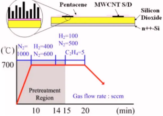
Figure 1 provides a schematic cross section of a BC pentacene TFT possessing an MWCNT S/D and the recipe
for growth of the MWCNTs. A n++-Si substrate was used as
the gate electrode. After standard cleaning, a 320-nm-thick SiO2 layer was grown thermally as the gate insulator. For S/D formation, an Fe/ Ti catalytic layer was then deposited through electron beam thermal evaporation and patterned us-ing the lift-off technique. For comparison, the Ti buffer layer was prepared at two different thicknesses 共10 and 50 nm兲, while the thickness of the Fe layer was fixed共5 nm兲. Subse-quently, the MWCNTs were grown through T-CVD; the pro-cedure was performed as follows: The samples were heated to 700 ° C under a nitrogen gas共N2兲 atmosphere. After pre-treatment of the Fe/ Ti catalytic layer in a mixed hydrogen 共H2兲 and N2 atmosphere, MWCNTs were grown on the S/D
region through pyrolysis of ethylene共C2H4兲, as the carbon
source, over two different growth times共3 and 5 min兲. The lengths of the MWCNTs deposited for 3 and 5 min were confirmed through scanning electron microscopy 共SEM兲 to be ⬃400 nm and 1m, respectively. A pentacene layer 共⬃40 nm兲 was finally deposited using thermal evaporation in a high vacuum chamber operated at a base pressure of
a兲Electronic mail: [email protected]
FIG. 1. 共Color online兲 Schematic cross-sectional depiction of a pentacene BC-OTFT possessing MWCNT S/D electrodes, and the recipe for the growth of the MWCNTs.
APPLIED PHYSICS LETTERS 91, 083502共2007兲
0003-6951/2007/91共8兲/083502/3/$23.00 91, 083502-1 © 2007 American Institute of Physics This article is copyrighted as indicated in the article. Reuse of AIP content is subject to the terms at: http://scitation.aip.org/termsconditions. Downloaded to IP:
10−6Torr at room temperature. The electrical properties of the fabricated OTFTs were characterized using a Kiethley 4200 parameter analyzer.
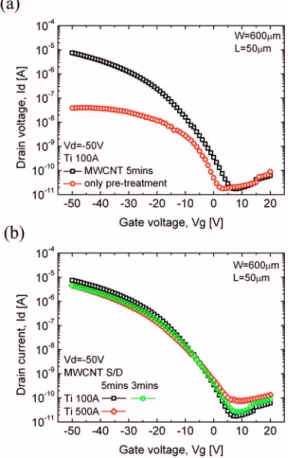
Figure 2共a兲 provides a comparison of the Id-Vg
charac-teristics of the OTFTs prepared with and without MWCNT coverage on the S/D region. It is clear that the performance of the OTFTs was improved significantly after incorporating the MWCNTs. We believe that this behavior is related to three factors:共1兲 the difference between the work functions of Fe 共⬃4.5 eV兲 and pentacene is larger than that between MWCNT 共4.7±0.4 eV兲 and pentacene;7 共2兲 the MWCNT/ pentacene system probably possesses better contact proper-ties than that of the metal/pentacene system, as might be expected from a previous finding that pentacene molecules, when deposited onto SWCNT electrodes, stack on the sur-face of the SWCNTs in a commensurate configuration as a result of favorable-interactions;9and共3兲 the contact area induced by the presence of MWCNTs was increased tremen-dously. All of these factors will contribute to the smaller contact resistance and, in turn, improve the device perfor-mance. Figure 2共b兲 depicts the Id-Vg characteristics of
OT-FTs prepared using different MWCNT growth times and Ti layer thicknesses. The device width共W兲 and length 共L兲 were 600 and 50m, respectively. Obviously, the BC-OTFT pre-pared with a longer MWCNT growth times and having a thinner Ti layer exhibited better performance; remarkably, its on/off ratio spanned six orders of magnitude. The effect of the Ti layer’s thickness presumably is due to the fact that a thicker Ti layer has a larger carrier injection barrier at the
interface with the pentacene active layer.10 In terms of the effect of the MWCNTs’ growth time, we suspect that a longer duration increased the length of the MWCNTs accord-ingly, providing a larger contact area between the pentacene layer and the MWCNT S/D electrodes. For OTFTs contain-ing a 10-nm-thick Ti layer and 5-min-grown MWCNT, we found that the best performance was a saturation mobility of 0.14 cm2/ V s at a value of Vdof −50 V when W and L were
75 and 50m, respectively; this value was extracted from the current equation,
Id=satCoxW共VGS− Vt兲2/2L,
wheresatis the saturation mobility, Coxis the capacitor per unit area 共cm2兲, Vt is the threshold voltage 关defined as the
voltage at which the drain current level is equal to I0共W/L兲兴,
and I0has the magnitude of 1.67⫻10−10A. It is noteworthy
that if the value of Vt were determined using maximum
transconductance共Gm,max兲 gear, the best value for the
satu-ration mobility would be three times larger. Figure3displays SEM images of the surface morphologies after the deposition of pentacene for the two MWCNT growth times. We observe that pentacene had coated both the MWCNTs and the cata-lytic metal surfaces, and that a longer duration of growth resulted in longer MWCNTs, as expected. Moreover, we found that the two samples possessed almost identical pen-tacene grain structures in the channel region and near the S/D region, i.e., the transition region. As a result, we suggest that the enhanced performance of our MWCNT S/D OTFTs arose mainly from the improved contact properties, rather than from carrier transport along the channel.
Figure4 displays the dependence of the total resistance
Rtotalon the channel length at different gate voltages for the
sample subjected to 5 min MWCNT growth. The drain volt-age was −5 V. For the channel gradual approximation2,3with S/D series resistance RSD, the value of Rtotalis given by
FIG. 2.共Color online兲 共a兲 Id-Vgcharacteristics of BC-OTFTs prepared with and without coverage of MWCNTs on the S/D region.共b兲 Id-Vg character-istics of BC-OTFTs plotted with respect to the MWCNT growth time and the Ti layer thickness. The channel width and length were 600 and 50m, respectively; the Ti layer was 10 nm thick.
FIG. 3. SEM images of the surface morphologies after the deposition of pentacene for samples prepared using共a兲 5 and 共b兲 3 min MWCNT growth. 083502-2 Chang, Chien, and Yang Appl. Phys. Lett. 91, 083502共2007兲
This article is copyrighted as indicated in the article. Reuse of AIP content is subject to the terms at: http://scitation.aip.org/termsconditions. Downloaded to IP: 140.113.38.11 On: Wed, 30 Apr 2014 07:02:17
Rtotal= VD/ID= Rch+ RSD= RSD+ L/关WlinCox共VG− Vt兲兴,
wherelinis the linear-region mobility. The extracted value of the total resistance from the intercept of linear fitting was ⬃3⫻108⍀m, which is one order of magnitude lower than
that of the sample subjected to 3 min MWCNT growth共data not shown兲.
In summary, we propose a simple and practical tech-nique for preparing T-CVD-grown MWCNTs as S/D elec-trodes in pentacene-based BC-OTFTs. We found that the
di-rect contact of the MWCNT electrodes with the pentacene channel provided excellent contact properties and a larger contact area, which, in turn, led to a relatively low contact resistance. As a consequence, the fabricated devices exhib-ited good electrical characteristics, i.e., high saturation mo-bilities and high on/off ratios.
The authors thank P. C. Chang for suggesting the proce-dure for growing the MWCNTs.
1D. J. Gundlach, T. N. Jackson, D. G. Schlom, and S. F. Nelson, Appl.
Phys. Lett. 74, 3302共1999兲.
2P. V. Necliudov, M. S. Shur, D. J. Gundlach, and T. N. Jackson,
Solid-State Electron. 47, 259共2003兲.
3D. J. Gundlach, L. Zhou, J. A. Nichols, T. N. Jackson, P. V. Necliudov,
and M. S. Shur, J. Appl. Phys. 100, 024509共2006兲.
4J.-P. Salvetat, J.-M. Bonard, N. H. Thomson, A. J. Kulik, L. Forró, W.
Benoit, and L. Zuppiroli, Appl. Phys. A: Mater. Sci. Process. 69, 255 共1999兲.
5L. Vaccarini, C. Goze, L. Henrard, E. Hernández, P. Bernier, and A.
Rubio, Carbon 38, 1681共2000兲.
6H.-C. Cheng, R.-L. Lai, Y.-R. Chang, K.-C. Lin, C.-P. Juan, P.-C. Chang,
C.-Y. Lee, and J.-K. Shiu, Jpn. J. Appl. Phys., Part 1 46, 863共2007兲.
7S. C. Lim, H. J. Jeong, K. S. Kim, I. B. Lee, D. J. Bae, and Y. H. Lee,
Carbon 43, 2801共2005兲.
8Y. Awano, S. Sato, D. Kondo, M. Ohfuti, A. Kawabata, M. Nihei, and N.
Yokoyama, Phys. Status Solidi A 203, 3611共2006兲.
9Q. Cao, Z.-T. Zhu, M. G. Lemaitre, M.-G. Xia, M. Shim, and J. A. Rogers,
Appl. Phys. Lett. 88, 113511共2006兲.
10N. Yoneya, M. Noda, N. Hirai, K. Nomoto, M. Wada, and J. Kasahara,
Appl. Phys. Lett. 85, 4663共2004兲. FIG. 4. Total resistance of the BC-OTFTs plotted as a function of the
chan-nel length.
083502-3 Chang, Chien, and Yang Appl. Phys. Lett. 91, 083502共2007兲
This article is copyrighted as indicated in the article. Reuse of AIP content is subject to the terms at: http://scitation.aip.org/termsconditions. Downloaded to IP: 140.113.38.11 On: Wed, 30 Apr 2014 07:02:17