Reliability Properties and Current Conduction Mechanisms of HfO2 MIS Capacitor
with Dual Plasma Treatment
Kow-Ming Changa,b, Ting-Chia Changa,*, Shou-Hsien Chena, and I-Chung Dengc
a Department of Electronics Engineering & Institute of Electronics, National Chiao Tung
University, 1001 Ta Hsueh Road, Hsinchu, Taiwan 30010, R.O.C.
b College of Electrical and Information Engineering, I-Shou University, Kaohsiung,
Taiwan 84001, R.O.C.
c Department of Electronic Engineering, Technology and Science Institute of Northern
Taiwan
The incorporation of nitrogen in HfO2 gate dielectrics has been
reported to be beneficial for electrical performance. The improvement in the electrical characteristics of HfO2 thin film with
plasma nitridation process or plasma fluorination process has also been examined. In this study, dual plasma, CF4 pre-treatment and
nitrogen post-treatment, treatments were performed on HfO2 MIS
capacitor for further improvement on reliability characteristic. We examine the reliability properties and the current conduction mechanism of HfO2 thin films. The frequency dispersion and
constant voltage stress (CVS) characteristics of the samples were analyzed to estimate the improvement. According to the present study, dual plasma treatment could be better than single plasma treatment and would be an effective approach for HfO2 dielectric
improvement.
Introduction
The rapid progress of complementary metal oxide semiconductor (CMOS) integrated circuit technology has met several serious technological challenges over the past few years. According to the prediction of the International Technology Roadmap for Semiconductor (ITRS), the conventional gate dielectric layer will reach its physical limits [1]. Gate dielectric scaling of CMOS will increase the speed and the packing density of modern circuits. However, the aggressive shrinking of the gate length and gate dielectric thickness accompanies excessive leakage current and reliability problems. To solve these problems, a major solution is to replace the traditional SiO2 or SiON by other higher
dielectric constant material. Using high dielectric constant material for gate dielectric could have larger physical thickness and maintain smaller equivalent oxide thickness (EOT). As a result, high-dielectric-constant (high-κ) thin films have been considered as suitable gate dielectric for modern CMOS technology. There are various high-κ thin film has been investigated [2-4]. Among these high-κ materials, HfO2 is considered as the
most promising candidate because of high dielectric constant (~25), wide band gap (~5.7 eV), and large band offset with Si conduction band (~1.5 eV) [2, 5]. Nevertheless, there are still some issues which need to be considered, such as the reliability and thermal stability of the dielectrics [6, 7].
It has been reported that nitrogen incorporated into HfO2 gate dielectrics has
beneficial effect on performance [8]. Nitrogen could be incorporated into dielectric layer by ICP plasma nitridation process at lower temperature [9, 10]. As reported in previous study: nitrogen incorporation can suppress crystallization during high temperature treatment, reduce dopant penetration, increase dielectric constant, and reduce leakage current by about 3-4 orders of magnitude [11, 12]. Umezawa et al [13] noted that nitrogen could deactivate the oxygen vacancy related states within HfO2 band gap. The
absence of gap states leads to the removal of electron leakage path.
In addition, the incorporation of fluorine in HfO2 gate dielectrics also has been
reported to be beneficial for electrical and reliability performance [14-16]. The quality of interfacial layer (IL) becomes more and more important due to gate dielectric scaling. Wong et al [17] noted that the applied electric field would be largely distributed in the low-κ region for high-κ/low-κ stack layer because of Gauss’s law. The first breakdown happened in the low-κ layer [17]. Recently, several studies have used fluorine incorporation to improve IL quality at HfO2/Si interface because Si-F bond (5.73 eV) is
stronger than Si-H bond (3.18eV) [18, 19]. Moreover, pre-CF4 plasma treatment has been
shown to effectively suppress the IL formation [20].
In this study, we propose to combine two kinds of plasma treatment (denoted as dual plasma treatment), CF4 pre-treatment and nitrogen post-treatment, in order to
achieve further improvement. We have examined the reliability properties and the current conduction mechanism of HfO2 MIS capacitor structure. First of all, the
capacitance-voltage (C-V) characteristics and current-capacitance-voltage (J-V) characteristics will be briefly described. Second, the frequency dispersion and constant voltage stress (CVS) characteristics of the samples will be analyzed to estimate the improvement. Finally, current conduction mechanisms, such as Schottky emission, Frenkel-Poole (F-P) emission, and Fowler-Nordheim (F-N) tunneling will be discussed. Schottky barrier height, F-P barrier height, and F-N barrier height will be extracted.
Experimental
After standard RCA cleaning, the samples were treated in CF4 plasma (denoted as
CF4 pre-treatment) for various times. The substrate temperature in a plasma enhanced
chemical vapor deposition (PECVD) system was set at 300 oC. The process pressure and the CF4 flow rate were 500 mTorr and 100 sccm, respectively. The RF power was set at
20 W and the exposure times were varied in the range of 10-40 sec. After CF4
pre-treatment, HfO2 thin film was deposited on the samples by the metal organic chemical
vapor deposition (MOCVD) system. Then post deposition annealing (PDA) was performed at 600 oC for 30 sec in a rapid temperature annealing (RTA) system. After PDA, samples were nitrided in nitrogen plasma (denoted as nitrogenpost-treatment) by PECVD. The flow rate of nitrogen gas, which is N2 or NH3,was set at 100 sccm. Post
nitridation annealing (PNA) was performed with RTA equipment at 600 oC for 30 sec in order to reduce plasma damage. Thereafter, 40 nm-Ti films and 400 nm Al films were deposited by e-beam evaporation system. The top electrodes were defined lithographically and etched to define a gate area of 5000 μm2. Finally, backside Al
electrodes were deposited by the thermal evaporation to form the Ohmic contact. The capacitance-voltage (C-V) and current-voltage (I-V) characteristics of MIS structure were measured by using a C-V measurement (Hewlett-Packard 4284) and Hewlett-Packard
4156C semiconductor parameter analyzer, respectively. The condition of frequency dispersion measurement was set as from 1 kHz to 100 kHz. The stress condition of CVS measurement was set as a constant voltage -3V for 0 to 500 sec. Furthermore, the I-V characteristics were measured at elevated temperatures from 25 to 125 oC, 25 oC per step, in order to analyze current conduction mechanisms.
Results and Discussion C-V and J-V Characteristics
Figure 1 shows the C-V characteristics of the HfO2 thin films treated in CF4
plasma for different process durations and N2 plasma for 120 sec. The frequency used in
the high frequency C-V measurement was set at 50 kHz. The sample was treated only in N2 plasma for 120 sec (RF power = 50 W) shows much higher capacitance density than
the sample with no treatment. The higher capacitance could be attributed to the PDA process [21-23] and the nitrogen incorporation in the HfO2 thin film. The nitrogen
incorporation could enhance the electronic polarization as well as the ionic polarization, which result in the increase of dielectric constant [12, 24]. On the other hand, the capacitance density and interface characteristics show further improvement with the combination of CF4 pre-treatment for 10 sec and N2 post-treatment for 120 sec. With CF4
pre-treatment, fluorine atoms would pile up at the HfO2/Si interface, improve the quality
of interface [19], and suppress the IL formation [20]. Besides, for CF4 pre-treatment
times longer than 10 sec, the plasma damage caused the degradation of HfO2/Si interface
and the degradation of capacitance density.
-2 -1 0 1 0.0 2.0x10⁻⁷ 4.0x10⁻⁷ 6.0x10⁻⁷ 8.0x10⁻⁷ 1.0x10⁻⁶ 1.2x10⁻⁶ 1.4x10⁻⁶ No treatment N2 50W 120s CF4 20W 10s+N2 50W 120s CF4 20W 20s+N2 50W 120s CF4 20W 30s+N2 50W 120s CF4 20W 40s+N2 50W 120s
Ca
pacitance
(F/cm
2)
Voltage (V)
Freq.=50 kHz
Figure 1. The C-V characteristics of the HfO2 thin films treated in CF4 plasma for
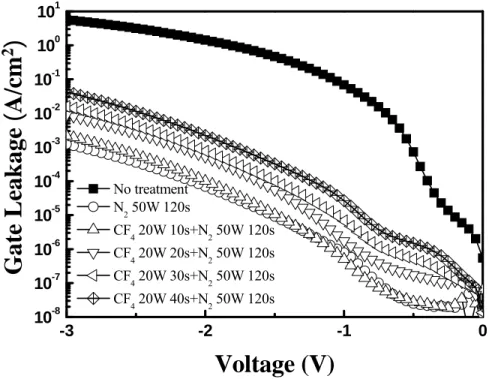
Figure 2 shows the J-V characteristics of the HfO2 thin films treated in CF4
plasma for different process durations and N2 plasma for 120 sec. Compared with the
sample with no treatment, the gate leakage current decreased by about 4 orders of magnitude for the sample with CF4 pre-treatment for 10 sec and N2 post-treatment for
120 sec. The reduction of the gate leakage could be attributed to defect passivation. Oxygen vacancy related states and interface states could be passivated by nitrogen and fluorine atoms [13, 16]. On the other hand, for CF4 pre-treatment times longer than 10 sec,
the plasma damage caused the degradation of interface and the increase of gate leakage current. The best condition of dual plasma treatment is as follows: CF4 pre-treatment
(time=10s, RF Power=20W) and N2 post-treatment (time=120s, RF Power=50W). The
gate leakage of the sample with best condition is 1.05 × 10⁻⁵ A/cm2 at Vg = -1.5 V.
-3 -2 -1 0 10-8 10-7 10-6 10-5 10-4 10-3 10-2 10-1 100 101 No treatment N2 50W 120s CF4 20W 10s+N2 50W 120s CF4 20W 20s+N2 50W 120s CF4 20W 30s+N2 50W 120s CF4 20W 40s+N2 50W 120s
Gate Leak
age
(A/
cm
2)
Voltage (V)
Figure 2. The J-V characteristics of the HfO2 thin films treated in CF4 plasma for
different process durations and N2 plasma for 120 sec.
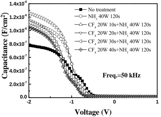
In Figure 3 and Figure 4, the C-V and the J-V characteristics of the HfO2 gate
dielectrics, treated in CF4 plasma for different process durations and NH3 plasma for 120
sec, are presented. The RF power of NH3 post-treatment was set at 40 W. As mentioned
before, the reason of the improvement in the NH3 plasma nitridation process could be the
same as the one in the N2 plasma nitridation process. From the similar analysis, the best
condition of dual plasma treatment is as follows: CF4 pre-treatment (time=10s, RF
Power=20W) and NH3 post-treatment (time=120s, RF Power=40W). The gate leakage of
the sample with best condition is 1.62 × 10⁻⁵ A/cm2 at Vg = -1.5 V. In summary, C-V and
-2 -1 0 1 0.0 2.0x10⁻⁷ 4.0x10⁻⁷ 6.0x10⁻⁷ 8.0x10⁻⁷ 1.0x10⁻⁶ 1.2x10⁻⁶ 1.4x10⁻⁶
Freq.=50 kHz
No treatment NH3 40W 120s CF4 20W 10s+NH3 40W 120s CF4 20W 20s+NH3 40W 120s CF4 20W 30s+NH3 40W 120s CF4 20W 40s+NH3 40W 120sCa
pacit
a
nce
(F/cm
2)
Voltage (V)
Figure 3. The C-V characteristics of the HfO2 thin films treated in CF4 plasma for
different process durations and NH3 plasma for 120 sec.
-3 -2 -1 0 10-8 10-7 10-6 10-5 10-4 10-3 10-2 10-1 100 101 No treatment NH3 40W 120s CF4 20W 10s+NH3 40W 120s CF4 20W 20s+NH3 40W 120s CF4 20W 30s+NH3 40W 120s CF4 20W 40s+NH3 40W 120s
Gate Leakage
(A/cm
2)
Voltage (V)
Figure 4. The J-V characteristics of the HfO2 thin films treated in CF4 plasma for
Frequency Dispersion Characteristics
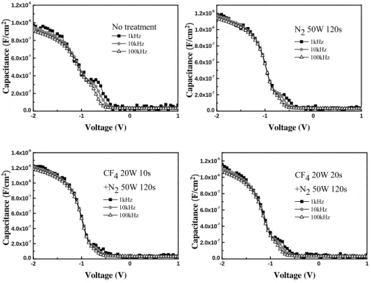
The C-V characteristics of the HfO2 thin films, treated with CF4 plasma for
different process durations and N2 plasma for 120 sec, have been measured as a function
of frequency as shown in Figure 5. The measurements were made in the frequency range of 1-100 kHz (1, 10, and 100 kHz). Frequency dispersion could be observed because of the response of trap charges to signal frequency. At low frequencies, interface traps generated the additional capacitance because some of traps could follow the change of gate voltage [25]. The frequency dispersion in the accumulation region and the hump in the depletion region are significant for the sample with no treatment. The sample treated by N2 plasma showed relatively smaller frequency dispersion and smaller hump than the
sample with no treatment. On the other hand, it was obvious that the sample treated by CF4 pre-treatment for 10 sec and N2 post-treatment for 120 sec exhibited nearly no
dispersion in the accumulation region and nearly no hump in the depletion because interface states could be improved effectively [25-28] by dual plasma treatment. However, the frequency dispersion and the hump became severe again when the CF4 pre-treatment
time is longer than 10 sec owing to plasma damage at interface.
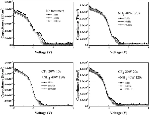
Figure 6 displays the C-V frequency dependence of the HfO2 thin films treated in
CF4 plasma for different process durations and NH3 plasma for 120 sec. The sample
treated by CF4 pre-treatment for 10 sec and NH3 post-treatment for 120 sec exhibited
nearly no dispersion and nearly no hump during C-V measurement. This indicated that dual plasma treatment could effectively eliminate interface states and greatly enhance IL quality than single plasma treatment.
Figure 5. C-V frequency dependence of the HfO2 thin films treated in CF4 plasma for
different process durations and N2 plasma for 120 sec.
-2 -1 0 1 0.0 2.0x10⁻⁷ 4.0x10⁻⁷ 6.0x10⁻⁷ 8.0x10⁻⁷ 1.0x10⁻⁶ 1.2x10⁻⁶ No treatment 1kHz 10kHz 100kHz Capacita nce (F/cm 2) Voltage (V) -2 -1 0 1 0.0 2.0x10⁻⁷ 4.0x10⁻⁷ 6.0x10⁻⁷ 8.0x10⁻⁷ 1.0x10⁻⁶ 1.2x10⁻⁶ N2 50W 120s 1kHz 10kHz 100kHz Capacitance (F/cm 2) Voltage (V) -2 -1 0 1 0.0 2.0x10⁻⁷ 4.0x10⁻⁷ 6.0x10⁻⁷ 8.0x10⁻⁷ 1.0x10⁻⁶ 1.2x10⁻⁶ 1.4x10⁻⁶ CF4 20W 10s +N2 50W 120s 1kHz 10kHz 100kHz Capacitance (F/cm 2) Voltage (V) -2 -1 0 1 0.0 2.0x10⁻⁷ 4.0x10⁻⁷ 6.0x10⁻⁷ 8.0x10⁻⁷ 1.0x10⁻⁶ 1.2x10⁻⁶ CF4 20W 20s +N2 50W 120s 1kHz 10kHz 100kHz Capacitance (F/cm 2) Voltage (V)
Figure 6. C-V frequency dependence of the HfO2 thin films treated in CF4 plasma for
different process durations and NH3 plasma for 120 sec.
Figure 7. The C-V curves before and after CVS characteristics of the HfO2 thin films
treated by (a) single plasma treatment and (b) dual plasma treatment. Constant Voltage Stress Characteristics
Figure 7 displays the C-V curves before and after CVS testing of the HfO2 thin
films treated by N2 plasma post-treatment (as shown in Figure 7(a)) and the combination
of CF4 plasma pre-treatment and N2 plasma post-treatment (as shown in Figure 7(b)),
respectively. The stress voltage was set at -3 V. The stress times were made in a range from 0 to 500 sec. All the C-V curves shift to left as stress time increase indicated that there were positive charges trapped in the high-κ dielectric layer. Trapping of positive charges could be explained by Anode hole injection model [29]. During constant negative bias stress at a fixed gate voltage, the injected electrons traveled through dielectric and
-2 -1 0 1 0.0 2.0x10⁻⁷ 4.0x10⁻⁷ 6.0x10⁻⁷ 8.0x10⁻⁷ 1.0x10⁻⁶ 1.2x10⁻⁶ (a) ΔV= 150 mV f=50kHz CVS@V= -3V Capacitance (F/cm 2) Voltage (V) N2 50W 120s 0s 50s 100s 150s 300s 500s -2 -1 0 1 0.0 2.0x10⁻⁷ 4.0x10⁻⁷ 6.0x10⁻⁷ 8.0x10⁻⁷ 1.0x10⁻⁶ 1.2x10⁻⁶ 1.4x10⁻⁶ (b) ΔV= 86 mV CF4 20W 10s +N2 50W 120s 0s 50s 100s 150s 300s 500s f=50kHz CVS@V=-3V Capacitance (F/cm 2) Voltage (V) -2 -1 0 1 0.0 2.0x10⁻⁷ 4.0x10⁻⁷ 6.0x10⁻⁷ 8.0x10⁻⁷ 1.0x10⁻⁶ 1.2x10⁻⁶ No treatment 1kHz 10kHz 100kHz Capacita nce (F/cm 2) Voltage (V) -2 -1 0 1 0.0 2.0x10⁻⁷ 4.0x10⁻⁷ 6.0x10⁻⁷ 8.0x10⁻⁷ 1.0x10⁻⁶ 1.2x10⁻⁶ NH3 40W 120s 1kHz 10kHz 100kHz Capacitance (F/cm 2) Voltage (V) -2 -1 0 1 0.0 2.0x10⁻⁷ 4.0x10⁻⁷ 6.0x10⁻⁷ 8.0x10⁻⁷ 1.0x10⁻⁶ 1.2x10⁻⁶ 1.4x10⁻⁶ 1.6x10⁻⁶ CF4 20W 10s +NH3 40W 120s 1kHz 10kHz 100kHz Capacitance (F/cm 2) Voltage (V) -2 -1 0 1 0.0 2.0x10⁻⁷ 4.0x10⁻⁷ 6.0x10⁻⁷ 8.0x10⁻⁷ 1.0x10⁻⁶ 1.2x10⁻⁶ 1.4x10⁻⁶ CF4 20W 20s +NH3 40W 120s 1kHz 10kHz 100kHz C a pacitance (F/cm 2) Voltage (V)
arrived at the interface. These electrons gained energy to liberate the hydrogen at the interface, leading to the generation of Si dangling bond. The liberated hydrogen diffused into the dielectric through the oxide field, trapped in the dielectric, leading to the creation of positively charged centers [30, 31]. The C-V curves had smaller Vfb shift and less
distortion for samples with dual plasma treatment, indicating that samples with dual plasma treatment had less interface trap charges generated at the dielectric/Si interface and had better reliability properties than samples with single plasma treatment.
Schottky Emission
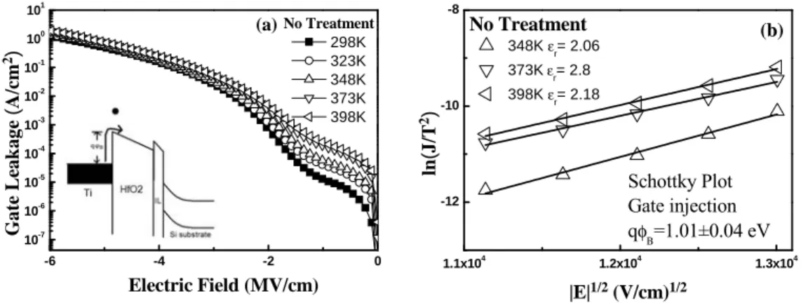
Figure 8(a) depicts the J-E plots for the sample with no treatment at different temperatures from 298 K to 398 K (25 K per step). The inset of Figure 8(a) is the band diagram demonstrating Schottky emission. The electric field E is an “effective” electric field (E = V/CET), while capacitance effective thickness (CET) is extracted from the capacitance density in the accumulation region [32]. The standard Schottky emission could be expressed as
(
)
⎥ ⎥ ⎦ ⎤ ⎢ ⎢ ⎣ ⎡− − = kT qE q T A JSE * 2exp φB 4πεrε0 , 0 * * 120 m m A = ( 2 2 K cm A ), (1)where JSE is the current density, A* is the effective Richardson constant, E is the effective
electric field, T is the absolute temperature, q is the electron charge, qφB is the Schottky
barrier height, k is Boltzmann’s constant, ε0 is the permittivity of free space, εr is the
dynamic dielectric constant, m* is the electron effective mass in HfO
2, m0 is the free
electron mass. The electron effective mass is 0.1 m0 [33, 34].
Figure 8. (a) The J-E curves at various temperatures and (b) Schottky emission plots, ln(J/T2) versus E1/2, for the HfO2 thin film with no treatment.
For the standard Schottky emission, a plot of ln(J/T2) versus E1/2 should be a straight line, as shown in Figure 8(b). It was found that Schottky emission is the dominate conduction mechanism in the region of low to medium electric fields (1.7 - 3.0 MV/cm) [35]. Eq. (2) expresses the intercept of the Schottky emission plot with the vertical axis. The barrier height can be extracted from Eq. (2).
-6 -4 -2 0 10-7 10-6 10-5 10-4 10-3 10-2 10-1 100 101 Ga te L eak ag e (A/cm 2) Electric Field (MV/cm) No Treatment 298K 323K 348K 373K 398K (a) 1.1x10⁴ 1.2x10⁴ 1.3x10⁴ -12 -10 -8 ln (J/ T 2) |E|1/2 (V/cm)1/2 No Treatment 348K εr= 2.06 373K εr= 2.8 398K εr= 2.18 Schottky Plot Gate injection qφΒ=1.01±0.04 eV (b)
( )
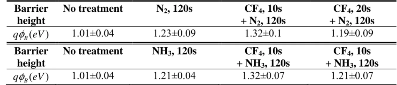
qkT A Intercept=ln * − φB , 0 * * 120 m m A = ( 2 2 K cm A ). (2) Because of effective electric field (E = V/CET), the extracted barrier heights in this study are effective barrier heights. The extracted Schottky barrier heights for the samples with no treatment, single plasma treatment, and dual plasma treatment are listed in Table I. It is clear that the samples had larger barrier height than other samples after CF4 pre-treatment for 10 sec and nitrogen post-treatment for 120 sec.TABLE I. Schottky Barrier Height Extracted for The Samples with No Treatment, Single Plasma Treatment, and Dual Plasma Treatment.
Barrier height No treatment N2, 120s CF4, 10s + N2, 120s CF4, 20s + N2, 120s ) (eV qφB 1.01±0.04 1.23±0.09 1.32±0.1 1.19±0.09 Barrier height No treatment NH3, 120s CF4, 10s + NH3, 120s CF4, 10s + NH3, 120s ) (eV qφB 1.01±0.04 1.21±0.04 1.32±0.07 1.21±0.07 Frenkel-Poole (F-P) Emission
When gate under negative bias, electrons will inject from gate into HfO2 dielectric
layer and will be trapped into shallow trap levels. Thereafter, the electrons transported through the dielectric layer by hopping between these trap levels, leading to leakage current, called Frenkel-Poole (F-P) emission. The standard F-P emission could be expressed as [35]
(
)
⎥ ⎥ ⎦ ⎤ ⎢ ⎢ ⎣ ⎡− − = kT qE q E C JFP t t r 0 exp φ πε ε , (3) where JFP is the current density, E is effective electric field, Ct is a constant proportionalto the density of bulk oxide traps, qφt is the trap energy in HfO2, and other parameters
are as defined earlier. For the standard Frenkel-Poole emission, a plot of ln(JFP/E) versus
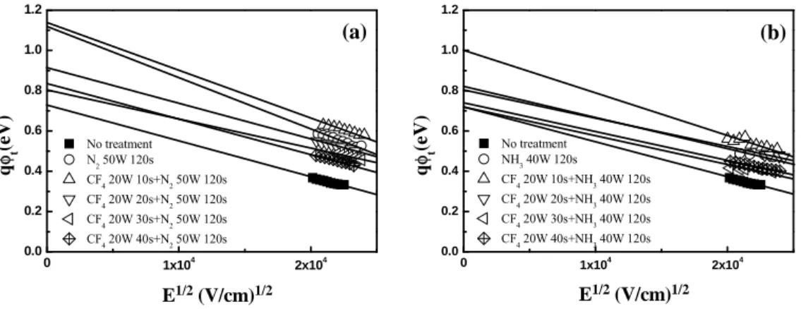
E1/2 should be linear. It was found that F-P emission is the dominate conduction mechanism in the region of medium to high electric fields (4.0 - 6.0 MV/cm). The trap energy in dielectric layer could be extracted form good F-P fitting, as shown in Figure 9.
Table II lists the trap energy levels of the samples with no treatment, single plasma treatment, and dual plasma treatment. The extracted trap levels for the sample with and without N2 post-treatment were 1.12 eV and 0.72 eV, respectively. In contrast,
the trap level for the sample treated by CF4 pre-treatment for 10 sec and N2
post-treatment for 120 sec was 1.14 eV. The deeper trap level means that most of shallow trap levels in HfO2 thin film can be eliminated [32] by using dual plasma treatment. The
elimination of shallow trap levels resulted in the reduction of F-P conduction current. Similarly, the sample treated in CF4 pre-treatment for 10 sec and NH3 post-treatment for
treatment could eliminate the shallow trap levels and greatly reduce the gate leakage current.
Figure 9. Trapping energy levels extracted from F-P fitting for the samples with dual plasma treatment (a) CF4 plasma and N2 plasma (b) CF4 plasma and NH3 plasma.
TABLE II. F-P Trapping Level Extracted for The Samples with No Treatment, Single Plasma Treatment, and Dual Plasma Treatment.
Barrier height No treatment N2, 120s CF4, 10s + N2, 120s CF4, 20s + N2, 120s
( )
eV qφt 0.72 1.12 1.14 0.91 Barrier height No treatment NH3, 120s CF4, 10s + NH3, 120s CF4, 10s + NH3, 120s( )
eV qφt 0.72 0.82 1.10 0.80 Fowler-Nordheim (F-N) TunnelingIn higher electric field, the Fowler-Nordheim (F-N) tunneling dominated the conduction mechanism [36]. The standard F-P emission could be expressed as
( )
⎥ ⎥ ⎦ ⎤ ⎢ ⎢ ⎣ ⎡− = qhE q m AE JFN f 3 2 8 exp 2 3 * 2 π φ , (4)where JFN is the current density, h is the Plunk’s constant, qφf is the potential barrier
height, m* is the electron effective mass in HfO2, and the other notations were as same as
mentioned before. The electron effective mass here is 0.1 m0 [33, 34]. If the leakage
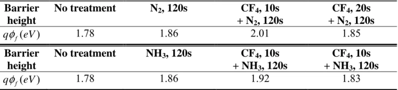
current is dominated by the F-N mechanism, a plot of ln(J/E2) versus 1/E should be linear. Linear characteristic could be observed at high electric field (> 7 MV/cm), as shown in Figure 10. The slope of each curve in Figure 10 and Eq. (5) could obtain the F-N barrier height, which were listed in Table III.
0 1x10⁴ 2x10⁴ 0.0 0.2 0.4 0.6 0.8 1.0 1.2 No treatment N2 50W 120s CF4 20W 10s+N2 50W 120s CF4 20W 20s+N2 50W 120s CF4 20W 30s+N2 50W 120s CF4 20W 40s+N2 50W 120s q φ t (e V) E1/2 (V/cm)1/2 (a) 0 1x10⁴ 2x10⁴ 0.0 0.2 0.4 0.6 0.8 1.0 1.2 (b) No treatment NH3 40W 120s CF4 20W 10s+NH3 40W 120s CF4 20W 20s+NH3 40W 120s CF4 20W 30s+NH3 40W 120s CF4 20W 40s+NH3 40W 120s q φt (e V) E1/2 (V/cm)1/2
(
)
23 * 2 2 128 9 slope q m h f ⎟⎟∗ ⎠ ⎞ ⎜⎜ ⎝ ⎛ = π φ . (5) Table III listed the F-N barrier height of the samples with no treatment, single plasma treatment, and dual plasma treatment. It could be observed that samples treated in CF4 pre-treatment for 10 sec and nitrogen post-treatment for 120sec had larger value thanother samples. The injection of electrons from the gate entered the conduction band of HfO2 by tunneling through a triangular potential barrier. The injected electrons interacted
with lattice or transferred its energy at anode [37], which resulted in the degradation of the dielectric layer. As a result, the sample with proper dual plasma treatment had bigger F-N barrier height and better reliability properties.
Figure 10. F-N tunneling characteristic, ln(J/E2) vs. 1/E, for the samples with dual plasma treatment (a) CF4 plasma and N2 plasma (b) CF4 plasma and NH3 plasma
TABLE III. F-N Barrier Height Extracted for The Samples with No Treatment, Single Plasma Treatment, and Dual Plasma Treatment.
Barrier height No treatment N2, 120s CF4, 10s + N2, 120s CF4, 20s + N2, 120s ) (eV qφf 1.78 1.86 2.01 1.85 Barrier height No treatment NH3, 120s CF4, 10s + NH3, 120s CF4, 10s + NH3, 120s ) (eV qφf 1.78 1.86 1.92 1.83 Conclusion
In conclusion, the reliability properties and current conduction mechanisms of HfO2 gate dielectric films as a function of dual plasma treatment (the combination of CF4
pre-treatment and nitrogen post-treatment) have been investigated. First, the best conditions which decided form C-V and J-V characteristics were the samples treated by CF4 plasma for 10 sec and N2 (NH3) plasma for 120 sec. According to the current
conduction analysis, the dominant current conduction mechanism was Schottky emission type in the region of low to medium electric fields (1.7 – 3.0 MV/cm); Frenkel-Poole (F-P) emission operated in the region of medium to high fields (4.0 – 6.0 MV/cm);
Fowler-0.06 0.08 0.10 0.12 0.14 -44 -40 -36 -32 No treatment N2 50W 120s CF4 20W 10s+N2 50W 120s CF4 20W 20s+N2 50W 120s CF4 20W 30s+N2 50W 120s CF4 20W 40s+N2 50W 120s Fowler-Nordheim Plot ln (J/ E 2) 1/|E| (cm/MV) (a) 0.06 0.08 0.10 0.12 0.14 -44 -40 -36 -32 Fowler-Nordheim Plot No treatment NH3 40W 120s CF4 20W 10s+NH3 40W 120s CF4 20W 20s+NH3 40W 120s CF4 20W 30s+NH3 40W 120s CF4 20W 40s+NH3 40W 120s ln (J/ E 2) 1/|E| (cm/MV) (b)
Nordheim (F-N) tunneling was dominant at high fields (> 7 MV/cm). Dual plasma treatment was effective in improving interface quality, eliminating shallow trap levels, and enhancing reliability properties. In summary, the effect of dual plasma treatment could be better than single plasma treatment and dual plasma treatment would be an effective technology to improve the reliability of HfO2 thin films.
Acknowledgments
The authors gratefully acknowledge the National Nano Device Laboratories (NDL) and the Nano Facility Center of the National Chiao Tung University.
References
1. International Technology Roadmap for Semiconductors, presented at public.itrs.net (2009).
2. G. D. Wilk, R. M. Wallace, and J. M. Anthony, J. Appl. Phys., 89, 5243 (2001). 3. Y. Shimamoto, J. Yugami, M. Inoue, M. Mizutani, T. Hayashi, K. Shiga, F. Fujita,
M. Yoneda, and H. Matsuoka, Symposium on VLSI Technology Digest of
Technical Papers, IEEE, p. 132, (2005).
4. C. Hobbs, L. Fonseca, V. Dhandapani, S. Samavedam, B. Taylor, J. Grant, L. Dip, D. Triyoso, R. Hegde, D. Gilmer, R. Garcia, D. Roan, L. Lovejoy, R. Rai, L. Hebert, H. Tseng, B. White, and P. Tobin, Symposium on VLSI Technology Digest
of Technical Papers, IEEE, p. 9, (2003).
5. J. Robertson, J. Vac. Sci. Technol. B, 18, 1785 (2000).
6. S. Yamaguchi, K. Tai, T. Hirano, T. Ando, S. Hiyama, J. Wang, Y. Hagimoto, Y. Nagahama, T. Kato, K. Nagano, M. Yamanaka, S. Terauchi, S. Kanda, R. Yamamoto, Y. Tateshita, Y. Tagawa, H. Iwamoto, M. Saito, N. Nagashima, and S. Kadomura, Symposium on VLSI Technology Digest of Technical Papers, IEEE, p. 192, (2006).
7. J.-P. Han, E. M. Vogel, E. P. Gusev, C. D’Emic, C. A. Richter, D. W. Heh, and J. S. Suehle, IEEE Electron Device Lett., 25, 126 (2004).
8. G. Shang, P.W. Peacock, and J. Robertson, Appl. Phys. Lett., 84, 106 (2004). 9. K.M. Chang, B.N. Chen, and S.M. Huang, Applied Surface Science, 254, 6116
(2008).
10. K.M. Chang, B.N. Chen, and C.K. Tang, ECS Trans., 19 (2), 773 (2009).
11. C. H. Choi, S. J. Rhee, T. S. Jeon, N. Lu, J. H. Sim, R. Clark, M. Niwa, and D. L. Kwong, Tech. Dig. - Int. Electron Devices Meet., 2002, 857 (2002).
12. M. Koyama, A. Kaneko, T. Ino, M. Koike, Y. Kamata, R. Iijima, Y. Kamimuta, A. Takashima, M. Suzuki, C. Hongo, S. Inumiya, M. Takayanagi, and A. Nishiyama,
Tech. Dig. Int. Electron. Device Meet., p. 849, (2002).
13. N. Umezawa, K. Shiraishi, T. Ohno, H. Watanabe, T. Chikyow, K. Torii, K. Yamabe, K. Yamada, H. Kitajima, and T. Arikado, Appl. Phys. Lett., 86, 143507 (2005).
14. C.S. Lai, W.C. Wu, J.C. Wang, and T.S. Chao, Appl. Phys. Lett. 86, 222905 (2005).
15. W.C. Wu, C.S. Lai, J.C. Wang, J.H. Chen, M.W. Ma, and T.S. Chao, J.
16. K. Tse and J. Robertson, Appl. Phys. Lett. 89, 142914 (2006).
17. H. Wong, B. Sen, V. Filip, and M. C. Poon, Thin Solid Films, 504, 192 (2006). 18. K.I. Seo, R. Sreenivasan, P.C. McIntyre, and K.C. Saraswat, Tech. Dig. - Int.
Electron Devices Meet, pp. 17.2.1–17.2.4., (2005).
19. C.S. Lai, W.C. Wu, K.M. Fan, J.C. Wang, and S.J. Lin, Jpn. J. Appl. Phys., 44, pp. 2307-2310, (2005)
20. C.S. Lai, W.C. Wu, T.S. Chao, J.H. Chen, J.C. Wang, L.L. Tay, and N. Rowell,
Appl. Phys. Lett. 89, 072904 (2006).
21. G. D. Wilk, M. L. Green, M.-Y. Hot, B. W. Busch, T. W. Sorsch, F. P. Klemens, B. Brijs', R. B. van Dover, A. Komblit, T. Gustafsson, E. Garfunkel, S. Hillenius, D. Monroe, P. Kalavade, and J.M. Hergenrother, Symposium on VLSI Technology
Digest of Technical Papers, IEEE, p. 88, (2002).
22. J. Molina, K. Tachi, K. Kakushima, P. Ahmet, K. Tsutsui, N. Sugii, T. Hattori, and H. Iwai, J. Electrochem. Soc., 154, 110 (2007).
23. C.C. Cheng, C.H. Chien, C.W. Chen, S.L. Hsu, C.H. Yang, and C.Y. Changa, J.
Electrochem. Soc., 153, 160 (2006).
24. M. R. Visokay, J. J. Chambers, A. L. P. Rotondaro, A. Shanware, and L. Colombo, Appl. Phys. Lett., 80, 3183 (2002).
25. H. X. Xu, J. P. Xu, C. X. Li, and P. T. Lai, Appl. Phys. Lett., 97, 022903 (2010). 26. T.M. Pan, C.S. Liao, H.H. Hsu, C.L. Chen, J.D. Lee, K.T. Wang, and J.C. Wang,
Appl. Phys. Lett., 87, 262908 (2005).
27. H. Kim, C. O. Chui, K. C. Saraswat, and P. C. McIntyre, Appl. Phys. Lett., 83, 2647 (2003).
28. H. Harris, K. Choi, N. Mehta, A. Chandolu, N. Biswas, G. Kipshidze, and S. Nikishin, Appl. Phys. Lett., 81, 1065 (2002).
29. D. J. DiMaria, E. Cartier, and D. A. Buchanan, J. Appl. Phys., 80, 304 (1996). 30. M. Houssa, J. L. Autran, A. Stesmans, and M. M. Heyns, Appl. Phys. Lett., 81,
709 (2002).
31. E. Efthymiou, S. Bernardini, J.F. Zhang, S.N. Volkos, B. Hamilton, and A.R. Peaker, Thin Solid Film, 517, 207 (2008).
32. W.C. Wu, C.S. Lai, T.M. Wang, J.C. Wang, C.W. Hsu, M.W. Ma, W.C. Lo, T.S. Chao, IEEE Trans. Electron Devices, 55, no. 7, pp. 1639–1646 (2008).
33. W.J. Zhu, T. P. Ma, T. Tamagawa, J. Kim, and Y. Di, IEEE Electron Device Lett., 23, 97 (2002).
34. F.C. Chiu, J. Appl. Phys., 100, 114102 (2006).
35. C.H. Liu, H.W. Chen, S.Y. Chen, H.S. Huang, and L.W. Cheng, Appl. Phys. Lett., 95, 012103 (2009).
36. F. El Kamel, P. Gonon, C. Vallée, and C. Jorel, J. Appl. Phys., 106, 064508 (2009).