Performance
Optimization by Wire and Buffer Sizing Under
the
Transmission
Line Model
*
Tai-Chen Chen' , Song-Ra Pan2, and Yao-Wen Changl
'Department
of
Electrical Engineering, National Taiwan University, Taipei 106, Taiwan{
d0943008, y w c h a n g}
@ cc .ee.ntu.edu.tw2 D e p a r t m e n t
of
C o m p u t e rand
Information Science, NationalChiao
Tung
University, H s i n c h u300, Taiwan
gis87528@cis.nctu.edu.t~
Abstract
As the operating frequency increases to Giga Hertz and the rise time of a signal is less than or comparable to the time-of-jiight delay of a line, it is necessay to consider the transmission line behavior for de- lay computation, We present in this paper an analytical formula for the delay Computation under the transmission line model. Extensive sim- ulations with SPICE show the high fidelity ojthe formula. Compared with previous works [S, I I ] , our model leads to smaller average errors in delay estimation. Based on this formula, we show the propern, that the minimum delay for a transmission line with rejection occurs when the number of round trips is minimized (i.e., equals one). Besides, we show that the delay of a circuit path is a posynomial function in wire and buffer sizes, implving that a local optimum is equal to the global optimum. Thus, we can apply any ejicient search algorithm such as the well-known gradient search procedure to compute the globally op- timal solution. Experimental results show that simultaneous wire and buffer sizing is venl effective for perjormance optimization under the transmission line model.
1 Introduction
As the operating frequency increases to Giga Hertz, the rise time of a signal is less than or comparable to the time-of-flight delay of a line. Also. the die size is getting larger, resulting in longer global intercon- nection lines. The trends make i t important to consider the transmis- sion line behavior for delay computation [l]. Transmission line effects become significant when t ,
<
2 t f , where t, is the rise time and t iis the time of flight determined by the wire length 1 divided by the ve- locity v [I]. There are two kinds of transmission lines. A line with negligible resistance is called a lossless transmission line. However,
on-chip interconnections have significant resistance, and they should be treated as lossy transmission lines [ I , 6, 191. Obviously, it is more accurate and desirable to consider line resistance for timing estima- tion and optimization. In this paper, therefore, we shall focus on lossy transmission lines.
When two transmission lines on a chip are connected and these two wires have different characteristic impedance, such mismatches
of
wire impedance can cause reflections at the junction point [ I , 131. Since re- flections may cause logic failure or increase delay, the discontinuties of impedance at junction points must be controlled in order to minimize the side effect of reflections. For a lossy transmission line, the ratio of the driving resistance to wire impedance determines the initial voltage generated on the wire. In addition to the ratio of the driving resistance to wire impedance, the number of round trips for the receiving end to reach its final value is determined by the voltage attenuation coeffi- cient which is a function of wire resistance and impedance. Since the voltage attenuation coefficient relates to the wire impedance, we can eliminate the reflections by matching the driving resistance and the wire impedance. The driving resistance of a gate and the impedance of a wire are approximately in inverse proportion to their sizes. Hence wire and gate sizing can affect the delay, implying that sizing circuit components (wires and buffers) is applicable to delay optimization.*This work was partially supported by the National Science Council of
Taiwan ROC under Grant No. NSC-89-2215-E-009-055.
Timing is a crucial concern in high-performance circuits. Many techniques such as wire sizing and gate sizing have been proposed to optimize timing (e.g., [3, 4, 5, 121, etc); however, most of the tech- niques are based on the Elmore delay model [8]. Modeling and analy- sis techniques for simulation and timing optimization under the lossy transmission line model have been studied extensively in the litera- ture [9, 10, 11, 14, 17, 18, 21, 24, 26, 27, 28, 29, 301. Previous work in [17, 211 proposed precise methods for simulating waveform, but they did not present any delay estimator. The work in [ 18, 281 mod- eled the transmission line effect; they, however, did not consider de- lay optimization. Several works in the literature consider the mini- mization of delay under the transmission line model. Gao and Wong in [9, 101 applied continuous wire-sizing to minimize delay under the lossy transmission line model: however, they focused o n exponentially tapered wires. Ismail and Friedman in [l 11 computed a uniform buffer size and the number of buffers to optimize the delay of a circuit path under the lossy transmission line model; however, their formula does not handle wire sizing. Lin and Pileggi in [14] proposed a wire sizing formulation with second order central moments, but their wire sizing formulation under the transmission line model is not always a posyn- omial program, and thus there is no optimality guarantee. T h e work in [26, 301 adopted the S-parameter macro delay model to minimize delay and skew, but the sensitivities were computed at each step using finite difference approximation which requires expensive computation.
The work in [24, 27, 291 adopted higher order moments to minimize delay, but their delay models were computationally expensive.
In this paper, we focus on delay modeling and timing optimization under the transmission line model. Unlike most previous works [ I 1, 14, 24, 26, 27.29, 301 that are based on relatively complicated models or incur larger errors, we present a simple, yet accurate formula for the delay computation under the lossy transmission line model. Extensive simulations with SPICE show that the formula has high fidelity, with an average error of within 6.85% for lossy transmission lines. Based o n this formula, we show the property that the minimum delay for a lossy transmission line with reflection occurs when the number of round trips is minimized (i.e., equals one). Besides, we show that the delay of a circuit path is a posynomial function in wire and buffer sizes, implying that a local optimum is equal to the global optimum. Thus we can apply any efficient search algorithm, such
as
the well-known gradient search procedure, to compute the optimal wire and buffer sizes for timing optimization for a circuit path. For a routing tree, we propose a two- stage algorithm to optimize the delay. In the first stage, we traverse the tree to determine its critical path and delay. In the second stage, w e control the reflections at all branching points to prevent from falsely triggering receivers and minimize the critical path delay. We repeat the two stages until no further improvements in the delay of the tree. Experimental results show that simultaneous wire and buffer sizing is very effective in minimizing the delays of circuit paths under the transmission line model.The remainder of this paper is organized as follows. Section 2 in- troduces some notation. Section 3 gives the gate and the transmission line models. Section 4 formulates the problem. Section 5 considers
the simultaneous wire and buffer sizing for delay optimization. Sec- tion 6 extends the cases on a general routing tree. Section 7 shows the experimental results, and finally concluding remarks are given in Section 8.
2
Notation
We use the following notation in this paper.
i b : the resistance of a gate with unit size.
rp: the resistance of gate i.
c^b: the capacitance of a gate with unit size.
cp: the capacitance of gate z.
9, : the size of gate z .
E W : the capacitance of a wire with unit size.
6,: the inductance of a wire with unit size. F W : the sheet resistance of a wire.
'tu;: the width of wire z .
2;: the length of wire z.
Z , : the characteristic impedance of wire z .
21%: the propagation velocity of wire z.
R,: the resistance of source.
CL : the capacitance of load.
VD D : the high voltage of power supply.
K :
the threshold voltage.( I ' , ~ : the transmission coefficient at point i if a signal is transmit- ted from point z to point j.
p,
.3 : the reflection coefficient at point z if a reflection travels from point z to point j.yt : the voltage attenuation coefficient on wire z if a signal is trans-
mitted from its source to sink.
Transmission Line Model
When the rise time of a signal is less than or comparable to the time-of-flight delay from one end of a wire to the other end, the wire should be modeled as a transmission line.
3.1
Gate and Wire Modeling
Figure 1 illustrates the gate and the lossy transmission line models used in this paper. For a gate z with size g , , the gate resistance rp is T ^ b / g ; and the gate capacitance cp is t b g , , where i b and E b are the unit-sized resistance and unit-sized capacitance of a gate, respectively. A uniform lossy transmission line z of width w , can be represented by a serial sections of unit-length resistance, i w /Tu;, unit-length induc- tance, ~ , , , / U J ; , and unit-length capacitance, t W , w u 1 , where i,, 60, and EW are the sheet resistance, the unit-sized inductance, and the unit- sized capacitance of a wire, respectively. The effect of inductance and capacitance can be represented by a characteristic impedance, Z , , which equals ~ ( 6 w / ~ w I ) / ( E w ~ ~ , ) = &/(zut&). The propaga- tion velocity of a wire i, U,, equals l/m [l]. If the length of a wire is I , , its total resistance, total inductance, and total capacitance are tW1, /,ut,, &,,1,
/
w t , and 2 , iu,Z,, respectively.Figure 1 : A gate is the loading of its upstream, but is the driver of its down- stream. A lossy transmission line is represented by a serial sections of its resis- tance, inductance, and capacitance, or we can merge each section of inductance and capacitance into a characteristic impedance.
Therefore, with the gate and the lossy transmission line models, we can represent a circuit path by resistors, capacitors, and characteristic impedance. Figure 2 illustrates the resulting circuit modeling for a circuit path with n buffers, where R s and CL are the resistance of source and the capacitance of load, respectively.
*
6
Figure
2:
A circuit path (with lossy transmission lines) is a combination ofresistors, capacitors, and characteristic impedances.
3.2
Reflections on a Wire
As shown in Figure 3, gate z
-
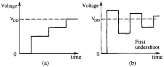
1 drives lossy transmission line z and gate z. In other words, the resistor with resistance rpb1 drives a lossy transmission line with the unit-length resistance ?,/wt, unit- length inductance iiw/w,, and unit-length capacitance 2,wt and a ca- pacitor with capacitance c!. Inductive and capacitive discontinuities may occur at the points 4 and B. Due to the inductive and capac- itive discontinuities, the resulting reflections may cause logic failure or excessively longer delay [ l ]. The initial voltage at the point B is the sum of the signal sent out from the point 4 and the reflection gen- erated at the point B. When the reflection generated at the point B travels backward to the point A , a new reflection generated at the point .4 is transmitted toward to the point B. The new voltage at the point B is the sum of the incoming reflection, the new outgoing reflection, and the initial voltage. As shown in Figure 4(a), the initial voltage at point B does not reach the threshold voltage. Thus, multiple round trips along the line may be required to correctly transmit a signal. As shown in Figure 4(b), if the reflection generated at the point A is neg- ative (rp-,<
Z;), the voltage may oscillate at the point B , causing overshoot or undershoor. This oscillating pattern is called ringing.Figure 3: The resistor with resistance rp-, drives a lossy transmission line with characteristic impedance 2, and a capacitor with capacitance cp.
Figure
4:
(a) Multiple trips are required to correctly transmit a signal. (b) Ringing may cause logic failures.3.3 Voltage Attenuation on a Wire
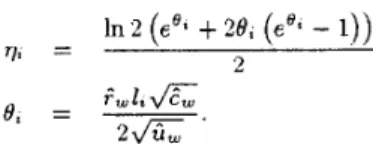
In a lossy transmission line, the resistance of a line causes voltage attenuation, and the voltage attenuation coefficient y1 along a lossy transmission line i is derived in [ l ] as follows:
Therefore, in Figure 3, the voltage at the point B before reflection is given by
V B = Y i V A . (2)
3.4
When to Use Transmission Line Analysis
cant when
According to [ 1, 15, 221, the transmission line behavior is signifi- t,.
<
2 t f , ( 3 )and
R1
5
2 Zo,where t , = 2 . 2 r ~ - l ( E Z U ~ I : , l t + c ~ ) i s t h e r i s e t i m e o f w i r e i ,
t / =
L , / u , is the time-of-flight delay, R1 = +,,,1,/?u, is the total resistance, andZO = Z, is the characteristic impedance. As illustrated in Figure 3, we can rewrite Inequalities (3) and (4) as Inequalities ( 5 ) and (6) as follows:
and
Besides, to make the voltage at the point B correctly drive the gate i, the voltage at the point B after infinite reflections should be greater than or equal to
V,.
In other words, the following inequality must be satisfied.V,
= 2 a , - l , L - / t ( l+
y f i ~ - i , ~+
~ : / ? - . l , ~+
. . . ) V D Dwhere
&i,&
7 , = 2 v G ,
Therefore, we should model a line as a lossy transmission line if
Inequalities (5)-(7) are satisfied; it should be modeled as a distributed
RC line, otherwise.
3.5 Delay Model
The time t , for charging the capacitive load (defined at SO% of the final value) of the lumped network equals In %R,CL, where R, is the pullup resistance and C L is the total capacitive load [19, 20, 251. Ac- cording to [I], the current that a lossless transmission line can supply is limited by its characteristic impedance. As a result, looking from the receiving end, the line behaves like a resistor with a value ZO. In a
lossy transmission line, not only its characteristic impedance, but also its partial resistance of the line that causes voltage attenuation supply the current. If the total resistance of a line causes voltage attenuation, the voltage at the receiving end becomes zero. In Section 3.3, we know that the voltage at the receiving end VB equals y,
VA.
This implies that there is only ( 1 -r l )
percentage of the total resistance for the line between nodes A and B , i, 1 ; / tu1, causing voltage attenuation.Consequently, the pullup resistance R, for the transmission line is equal to the sum of the characteristic impedance of the line, and partial resistance of the wire which causes voltage attenuation. We have the pullup resistance R, for the line as follows:
Hence, the time t , for charging the capacitive load of a transmission
line is given by
(9)
P w i , &
With a t - l , , = Z,/(rf-.i
+
Zc), y 2 = e 2 6 , and the effect ofreflection, the final voltage, V h D , at the receiving end after reflection
Table 1 : RC parameters of the 0.13 p m technology i n SlA'99
equals = ? y , Z , / ( r ~ - ,
+
Zt), which may not equal V D D Thus, we can use an approximate method that divides t , by the final voltage,vAD,
to obtain the charging time. t l , for which the voltage equals 0 5vD D Therefore, we havewhere
Because transmission line analysis always gives the correct answer independent of the rise time of the driver, delay is the sum of the time- of-flight t j along the wire and the time t,: for charging the capacitive
load [ I , 191. Thus, the propagation delay A(gt-.l. gl) from the gate gt-l to the next gateg, in Figure 3 is given by
where n is the number of required round trips to correctly transmit a sign a I.
3.6
Accuracy
We used SPICE to verify the accuracy of our delay model. The experiments were performed on a signal wire with no butTers. The pa- rameters we used are listed in Table l . The unit capacitance t, of a wire, the unit inductance 6, of a wire, the sheet resistance r*, of a wire, the unit capacitance
&,
and resistance ?b of a gate, the resistance of source R,, and the load capacitance C'L are 0.06 f F / p m ' , 1.667p H / D , 0.043 R I D , 1.17 f F / p m , 3.6 kR . pm? 750 R, and 23.4 f F , respectively. This set of parameters is based on the 0.13 pm technol- ogy of the S I N 9 9 roadmap [23].
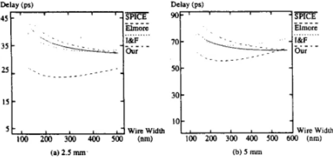
In the first and second experiments, we used fixed wire lengths (2.5
rnm & 5 m m ) with a variety of wire widths. The wire widths for all experiments satisfy Inequalities (5)-(7). Therefore, the wire widths ranged from 130 nrn to 480 nm for the first experiment, and ranged from 130 nm to 530 nm for the second experiment. In Figure 5 , the delays are plotted as functions of the wire widths for SPICE, Elmore, l&F, and our delay models, where I&F denotes the delay model pre- sented in [ l 11. Compared to SPICE and based on the lossy transmis- sion line of 2.5 'mm ( 5 mm) long, the maximum error calculated by the Elmore delay model is -36.13% (-19.58%) and the average error is 29.20% (12.05%), the maximum error calculated by the I&F delay model is -6.23% (1 1.34%) and the average error is 2.98% (4.70%), and the maximum error calculated by our delay model is 6.58% (12.38%) and the average error is 3.80% (6.22%).
In the third and fourth experiments, we used fixed wire widths (500
nm & 130 nm) with a variety of wire lengths. As mentioned earlier, the wire lengths for all experiments satisfy Inequalities (5)-(7). There- fore, the wire lengths ranged from 3.7 mm to 6.2 mm for the third experiment, and ranged from 0.82 mm to 7.75 mm for the fourth ex- periment. In Figure 6, the delays are plotted as functions of the wire lengths for SPICE, Elmore, I&F, and our delay models. Compared 194
to SPICE and based on the lossy transmission line of 500 nrn (130
n m ) wide, the maximum error calculated by the Elmore delay model is -10.01% (-51.74%)and theaverageerroris4.11% (28.11%), themax- imum error calculated by the I&F delay model is 10.99% (-14.19%) and the average error is 9.52% (5.30%), and the maximum error cal- culated by our delay model is l .99% (22.47%) and the average error is
1.49% (1 2.22%).
I
I - - . _ _ . . - - - -
I I
(a) 2.5 nun (b) 5 mm
Figure
5 : Comparison of the delays calculated by SPICE, Elmore, I&F, andour delay models for lossy transmission lines; (a) wire length = 2.5 m m ; (b) wire length = 5 mm.
(a) 500 nm (b) 130nm
Figure
6: Comparison of the delays calculated by SPICE, Elmore, 1&F, andour delay models for lossy transmission lines; (a) wire width = 500 n m ; (b) wire width = 130 nm.
According to the above four experiments, our delay model has the maximum inaccuracy at the minimum wire size and the average error is 6.85% under the lossy transmission line model. In particular, the delays computed from our model are always upper bounds of those obtained by SPICE, which makes
our
modela
reliable delay estima- tor under the lossy transmission line model. The Elmore delay model, however, has a significant negative percentage of errors. Therefore, the Elmore delay model is not a suitable delay estimator for the lossy trans- mission line model. Also, the I&F delay model incurs positive as well as negative errors for different wire widths of the same length. Hence, although the I&F delay model may be more accurate in some comer cases, it is less suitable for delay estimation under the lossy transmis- sion line model when we apply wire sizing to optimize a circuit. Often circuit designers prefer overestimating delay to underestimate, since an over-optimistic estimation of delay may lead to timing violations. Therefore, our delay model should be more suitable than the Elmore and I&F delay models for practical applications.4 Problem Formulation
This paper targets at minimizing delay by sizing circuit compo-
rn Input: A circuit path and the lower and upper bounds for wire
Objective: Determine the optimal wire and buffer sizes for each We will reformulate this problem for a routing tree in Section 6. nents. We formulate this problem as follows:
and buffer sizes.
segment in a circuit path, so that delay is minimized.
5
5.1 Reflection Considerations
In practice, designers typically desire to optimize performance without generating undesirable reflections and transmit a signal cor- rectly within a limited number of round trips. As the VLSI technology advances, the wire length is increasing and the capacitance of a gate is decreasing, making the time-of-flight delay dominate the delay. There- fore, we have the following theorem for the optimal number of round trips for delay optimization.
Theorem 1 The minimum delay for a circuit path with rejection oc- curs when the number of round trips equals one.
Optimal Wire and Buffer Sizing for a Path
Thus, we can rewrite Equation (1 1) as follows:
where
5.2 Optimal Wire Sizing
In this section, we minimize the delay of a circuit path by wire sizing. If all buffer sizes and locations are fixed, the delay function of a circuit path from the source s to sink t with n
+
1 segments ( W I , . . . ,can be calculated as follows:
/
(13) where
Notice that Equation (13) is a posynomial function in ' 1 1 ~ 1 , . . .,
Z O , + ~ , implying that the wire-sizing problem has a unique global min-
imum [2, 71. Thus, we can apply any efficient search algorithm, such as the well-known gradient search procedure, to find a locally optimal solution and thus the globally optimal solution.
Theorem 2 WithJixed buffer sizes and locations, the delay of a circuit path is a posynomial function in wire sizes.
5.3 Optimal Buffer Sizing
In this section, we minimize the delay of a circuit path by buffer sizing. If all wire sizes and buffer locations are fixed, the delay function of a circuit path from the source s to sink t with n
+
1 segments ( g ~ , . . . , g,) can be calculated as follows:n I . r ,
where
+d,&
2 6
8, = -.
Notice that Equation (14) is also a posynomial function in 91. . . ., gn. implying that the buffer-sizing problem has a unique global mini- mum [2, 71. Thus, we can apply any efficient search algorithm, such as the well-known gradient search procedure, to find a locally optimal solution and thus the globally optimal solution.
Theorem 3 With fixed wire sizes and buffer locations, the delay of a circuit path is a posynornialficnction in buffer sizes.
5.4
Optimal Simultaneous Wire and Buffer Sizing
In this section, we minimize the delay of a circuit path by simul- taneous wire and buffer sizing. If all buffer locations are fixed, the delay function of a circuit path from the source s to sink t with 2n
+
1 segments (w1. . . ., iun+1, 91, . . . , gn) is the same as Equation (14).Notice that Equation (14) is also a posynomial function in
w ,
. . .,w n + l , g l , . . ., gn. implying that the simultaneous wire- and buffer-
sizing problem has a unique global minimum [ 2 , 71. Thus, we can apply any efficient search algorithm, such as the well-known gradient search procedure, to find a locally optimal solution and thus the glob- ally optimal solution.
Theorem 4 With fixed buffer locations, the delav o f a circuitpath is a posynomialfunction in wire and buffer sizes.
6
Extensions to Wire and Buffer Sizing for
a
Routing Tree
Given a routing tree, our objective is to minimize the critical path delay under the constraints that the first undershoot at each branching point is within the same signal level, and the number of round trips required for correctly transmitting a signal from the root to each load is at most one. We formulate this problem as follows:
Input: A routing tree and the lower and upper bounds for wire and buffer sizes.
Output: Determine the optimal wire and buffer sizes of the tree, so that the critical path delay is minimized under the constraints that the first undershoot is within the same signal level, and the number of round trips is at most one.
We shall first discuss the problem on binary routing trees, and then apply the technique to general routing trees.
6.1 Reflection Constraints
As shown in Figure 7, when a signal is sent out from the source
R s and passes through the point 1 to the point 2, a reflection may be
generated at the point 2 and travels backward to the point 1. When the reflection reaches the point 1, the voltage at the point 1 will be inter- fered. What is worst, if a reflection propagated down to one load is large enough, it could cause logic failure at the load. To prevent from
Figure 7:
A signal is sent out from the point 0 and then passes through the point 1 to the point 2.falsely triggering the load, the reflection coefficient at each node must be large enough. For the example shown in Figure 7, if the reflec- tion coefficient p1.0 at the point 1 is larger, the reflections generated at
the points 2 and 3 have smaller impact on the point 1. The reflection coefficient p1.0 is given by
(15) By Equation (13, p1.0 becomes larger when Z1
ZZ
and 21 Z3 are smaller. If p1.0 becomes larger, the transmission coefficient a z . 1 =z1 z , ~ , f ~ ~ ~ + z,z3 is smaller. When a reflection generated at the point 2 travels backward to the point 1, the impact of the reflection may be negligible if a z . 1 is small enough. Similarly, the impact of the reflec-
tions generated at the point 3 on other points can also be negligible. For each point i of a routing tree, if the reflections generated at the point i have little interference at other points, a signal can be correctly transmitted from the source to the loads. In order to correctly trans-
F i g u r e 8: A signal is sent from the point i
-
1 to the point i, and then t+
1 and z+
2. The impact of the reflections generated at the points d+
1 and i+
2on the point i may be negligibleif 01,+1., and cy,+z., are small enough.
mit a signal from the source of a routing tree to each load, the voltage at each branching point must be larger than or equal to the threshold voltage Vt within one round trip. As shown in Figure 8, the following
constraint must be satisfied for the point z:
mi-l.:ye,-1,,(1 + 0 i , i - 1 )
2
V,. (16)Based on Inequality (1 6), the initial voltage at the point z will be greater than or equal to the threshold voltage when a signal from the point i - 1
arrives at the point z. Let e,.J denote the edge between the points i and j, and T ~represent the length of . ~ Since T , - I , , , ~ , . i + l , and ri.,+z
in Figure 8 could be different, the reflections generated at those points will arrive at the point i at different times. Without loss of generality, assume that T,,,+I
5
~ , . i + z5
~ i - 1 , ~ . The first reflection arrives at thepoint i is sent out from the point i
+
1, next is from the point i+
2, and the last is generated from the pointi
-
1.In
order to prevent the reflections from changing the signal level at the point z, w e have the following constraints:* . - 1 , , 7 c , - I , , ( 1 + & , , - 1 + ~ ~ , , + l - f ~ , , , + l ~ , + 1 , , ~ * , , - l ~ 2 vc (17) (18) (19) Iclt-hmdslkof(l7)
+
" , - I , ,-fez- ,, a,, , + ~ 7 2 , , , + , B,+z,, a.,.- I 2 Vclell.hmdrideof ( 1 8 )
+
- , - 1 , , 7 ~ , - ~ , , B ,,,- i P , - i , , ( 1+
b i , , - i ) t vc. If all constraints are satisfied, the reflection coefficient at each point will be large enough, implying that the reflections generated at the point i have little interference at other points. As a result, a signal can be correctly transmitted from the source to the loads in a tree.6.2 Delay Calculation
Given a routing tree, we number its nodes level by level, and from left to right on each level (see Figure 7). Let m , L , and
P
denote the number of edges in the tree, the set of loads, and the critical path, re- spectively. Similar to Equtaion (1 l), the critical path delay of a routing tree from the source s to a load t is given byAlgorithm F~nd-Cnizcal-Parh(T) Input: T-a routing tree
Output: the critical path begin
1 for each edge e , In T 2
3 Label e , with the weight n , r,
,
45 return the longest path end
Determine the number of round trips n , on e r
,
Call a depth-first traversal to find the longest path
Figure 9: The Algorithm for determining the cntical path of a tree.
where
c L denotes the capacitance of node i, U!,, and Z,,, denote the propaga- tion velocity and the impedance of edge e,,, , respectively.
We propose Algorithm Find-Critical-Path (summarized in Fig-
ure 9) to find the critical path of a routing tree T . First, we determine the number of round trips n,,] along edge e,,, required to correctly transmit a signal (Line 2 ) . The number of round trips is the minimum
r i t , 3 that satisfies the following constraint:
After determining the number of round trips on each edge, we label each edge with the weight n t , 3 T,,, (Line 3). The critical path delay is the sum of edge weights along the longest path. We then apply the depth first traversal to compute the longest path in O ( p ) time, where p
is the number of nodes (Line 4).
6.3
General Routing Tree
r-'
i+l i+2 i+k
Figure 10: The point z has k children. and the signal is sent from the point
1 - 1 to other points
We extend the technique discussed in previous subsections to gen- eral routing trees. As shown in Figure IO, assume that the point i has k children, and a signal is sent out from the point z - 1 and then prop- agates down to the children of the point i. Without loss of generality, assume that r t , t + i
5
T , . , + P5
. .
.5
rt.++5
~ ~ - 1 . ~ . To prevent the reflections generated at the children from changing the signal level atAlgorithm: Minimize-Tree-Delay(T) Input: T-a routing tree.
Output: wire sizes 4 = ( w I , i u z ,
.
. , ,wn) begin1 repeat
2 criiical-paih t Find-Critical-Path(T) .
3 'tu t Gradient-Search-P rocedure(criiica1-path)
4 end
until no improvement on the delay of
T
Figure 1 1 : The Alogrithm for minimizing the delay of a tree.
the point 2 , we have the following constraints:
a % - l , , 7 e , - l , i l t $ , , t - l t a,,,+1-Y:* , L , t % + l , t % % - l ? "t
If all constraints are satisfied, the reflection coefficient at each point will be large enough; thus, a signal can be correctly transmitted from the source to the loads in a general routing tree.
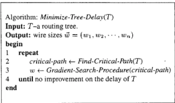
6.4 Our Algorithm
Our objective is to minimize the critical path delay of a routing tree under the constraints that a signal can be correctly transmitted within one round trip and the reflection is sufficiently small to pre- vent from falsely triggering loads. Since the delay of a tree is domi- nated by the critical path delay, our problem is to find the wire sizes
II? = ( ~ 1 , ~ 2 ' ' ,, ,(Un) that minimize the critical path delay A ( s , t ) of a tree subject to the constraints listed in Inequalities (16)-( 19). We can apply any search algorithm such as the well-known gradient search procedure to find a solution. Algorithm Minimize-Tree-Delay com-
putes the minimum delay of a routing tree (see Figure 11). It consists of two stages. The first stage applies the procedure Find-Critical-Path
to compute the critical path of a routing tree. The second stage applies the gradient search procedure to determine the wire sizes that minimize the critical path delay. We repeat the two stages until no improvements on the delay of the tree.
6.5 Simultaneous Wire and Buffer Sizing for a Rout-
ing Tree
Based on the gate and wire models presented in Section 3, we can divide a buffered routing tree into subtrees. In Figure 12, the rout- ing tree is divided into three subtrees. We can treat each subtree as a routing tree with no buffers, and then obtain the reflection constraints for each subtree. Thus, we can minimize the delay of a buffered rout- ing tree under the constraints that a signal can be correctly transmitted within one round trip, and the first undershoot is controlled to prevent from changing the signal level if the reflection constraints for each sub- tree are satisfied.
7
Experimental Results
of simultaneous wire and buffer sizing in performance optimization under the transmission line model.References
[ I ] H. B. Bakoglu, Circuir. Interconnections and Puckuging fur VLSI, Addison-Wesley
Publishing Company, Inc., 1990.
[2] M. S. Bazaraa. H. D. Sherali. and C. M. Shelty. Nonlinear Programming: T h e o n
andAlgurirhms. John Wiley and Sons, Inc., NY, 1993.
[3] C. P. Chen, Y. P. Chen. and D. F. Wong, "Optimal Wire-Sizing Formula Under the Elmore Delay Model,'' Proc. DAC. pp 487-490, June 1996
[4] C. P. Chen. C C. N. Chu, and D. F Wong, "Fast and Exact Simultaneous Gate and Wire Sizing by Lagrangian Relaxation," Proc. ICCAD, pp. 617-624.Nov 1998 [5] C. C. N. Chu and D. F. Wong, "A Polynomial Time Optimal Algorithm for Simul-
taneous Buffer and Wire Sizing." Proc. DATE. pp. 4791185. 1998.
[6] A. Deutsch, Gerard V. Kopcsay. Phillip I . Restle, Howard H. Smith. G. Katopis. Wiren D. Becker, Paul W Coteus, Christopher W. Surovic. Barry 1. Rubin, Richard P Dunne. Jr., T. Gallo. Keith A. Jenhns. Lewis M Terman. Robert H. Den- nard, George A. Sai-Halasz, Byron L Krauter. and Daniel R. Knebel, "When are Transmission-Line Effects Important for On-Chip Interconnections?". IEEE Trans. on Micmwave T h e o n und Techniques, vol. 45, pp. 1836-1 846, Oct. 1997.
[7] R. 1. Duffin. E. L. Peterson, and C. Zener, Geometric Programming: T h e o n and
Applicarion. John Wiley & Sons, Inc.. NY, 1967.
[8] W. C. Elmore. "The Transient Response of Damped Linear Networks with Panicu- lar Regard to Wide Band Amplifiers,'' J. Applied Physics, Vol. 19, No. I , 1948. [9] Y. Gao and D. F. Wong, "Shaping a VLSI Wire to Minimize Delay Using Transrms-
sion Line Model."Proc. ICCAD, pp. 61 1-616, Nov. 1998.
[IO] Y. Gao and D F Wong "Wire-sizing for Delay Minimization and Ringing Control Using Transmission Line Model,'' Proc. DATE, pp 512-5 16,2000.
[I I ] Y. 1. lsmail and E. G. Friedman. "Effects of Inductance on the Propagation Delay and Repeater Insertion in VLSI Circuits," IEEE TVLSI. vol. 8, no. 2. April 2000. [I21 H. R. Jiang. J. Y. Jou, and Y. W. Chang. "Noise-Constrained Performance Opti-
mization by Simultaneous Gate and Wire Sizing Based on Lagrangian Relaxation,"
Pruc. DAC. pp. 90-95. June 1999.
[I31 J. Lee and E. Shragowitz, "Overshoot and Undershoot Control for Transrmssion Line Interconnects." Pruc. ECTC, pp 879-884. 1999
[I41 T. Lin and L. T. Pileggi, "RC(L) Interconnect Sizing with Second Order Consider- ations via Posynomial Progrlunming."Pruc. ISPD. pp. 16-21. Apnl 2001
[ 151 F. Moll. M. Roca, A. Rubio. "Inductance in VLSI interconnection modeling;' Proc.
uf IEE Cirruirs, DevicesandSysrems, vol. 145. issue 3 . pp. 175-179. June 1998.
[ 161 S G. Nash and A Sofer. Linear and Nonlinear Prugramming. McGraw-Hill. Inc..
1996.
[I71 L. T Pillage and R. A. Rohrer. "Asymptotic Waveform Evaluation for Timing Anal- ysis," IEEE TCAD, Vol. 9. No 4, pp. 352-366, April 1990.
[IS] R. Gupta. L. Pileggi, "Modeling Lossy Transrmssion Lines Using the Method of
Characteristics." IEEE TCAS-I, Vol. 43. No. 7 , pp. 580-582. July 1996.
[ 191 Jan M. Rabaey. Digiral lnreyrared Circuirs: A Design Perspecrive. Prentice Hall. Inc.. 1996.
[20] I . Rebinstein. P. Penfield, Jr.. and M. A. Horowitz, "Signal Delay in RC Tree Net- works,"/€€€ TCAD. Vol. CAD-2. pp. 202-21 I . July 1983.
[21] J. S . Roychowdhury, A. R. Newton. and D. 0. Pederson. "Algorithms for the tran- sient simulation of lossy interconnect."/€€€ TCAD, vol 13. pp. 96-104, Jan. 1994. [22] K. L. Shepard, D Sitaram. and Yu Zheng. "Full-chip. three-dimensional. shapes-
based RLC extraction." Pruc. ICCAD, pp. 142-149. 2ooO.
[ 231 Senuconductor Industry Association. lnrernariunal Technulog? Roudmap for Srmi-
coriducrors 1999 Edition, Nov. 1999.
[24] Y Sugiuchi. B. Katz. and R. A. Rohrer. "Interconnect Optirmzation using Asymp- totic Waveform Evaluation(AWE)." Pruc. MCMC. pp 120-125. 1994. [25] Wayne Wolf, Modern VLSl Design: Sysrems on Silicon, 2nd Editon Prentice Hall.
Inc.. 1996.
[26] J. S. H. Wang and W W. M. Dai. "Optimal Design of Self-Damped Lossy Trans- mission Lines for Multichip Modules," Pruc. ICCAD, pp. 594-598, 1994. [27] T. Xu, E. S. Kuh, and Q. Yu, "A Sensitivity-Based Wiresizing Approach to Inter-
connect Optimization of Lossy Transmission Line Topologies." Proc. M C M C , pp. 117-122,1996.
[28] Q Yu and E. S. Kuh. "Exact Moment Matching Model of Transrmssion Lines and Application to Interconnect Delay Estimation." IEEE TVLSI, Vol. 3. No. 2. pp. 3 1 1- 322. June 1995
[29] Q. Yu. E. S. Kuh, and T. Xu. "Moment Models of General Transmission Lines with Application to Interconnect Analysis and Optirmzation." IEEE TVLSI. Vol. 4. No. 4. pp. 4771194, Dec. 1996.
[30] ' Q. Zhu. W. W. M. Dai. and J G. Xi, "Optimal Sizing of High-speed Clock Net-
works Based on Distributed R C and Lossy Transmission Line Models." Proc. IC-
CAD, pp. 6 2 8 6 3 3 . 1993.
[31] Q. Z h u and W. M. Dai, "High-speed clock network sizing optirmzation based on distributed R C and Lossy RLC interconnect models." IEEE TCAD. vol. 15, no 9. pp. 1106-1118,Sep. 1996.
(a) 2.5 nun
(C) 10 nun (d) IS m m
Figure
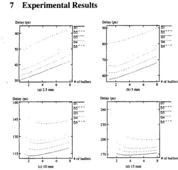
13: Comparison of different optimization techniques; D1: simultane-ous wire and buffer sizing; D2 & D3: wire sizing alone, and the gate resistances are 90 R and 60 R, respectively; D4 & D5: buffer sizing alone, and the wire widths are 0.3 p m and 0.13 p m , respectively.
We used the nonlinear programming solver, the LINGO 6.0 system, on an Intel Pentium I1 400 MHz PC to compute the optimal wire and buffer sizes in a circuit path. All computations are less than 1 sec. The parameters used are listed in Table 1.
Given four lines of the lengths 2.5 mm, 5 mm, I O m m , and
15 m m , we inserted a specified number of buffers at equidistance.
Then, we applied wire a n d o r buffer sizing to minimize delay. In Fig- ures 13(a), (b). (c), and (d), the path delays are plotted as functions of the number of buffers for the five optimization techniques D I , D2, D3, D4, and D5. D1 gives the delays by sizing wires and buffers simultane- ously (denoted by SWBS). D2 (D3) gives the delays that is optimized by sizing wires alone (denoted by WS) with the resistance of each gate equal to 90 R (60 0 ) . D4 (D5) gives the delays by sizing buffers alone (denoted by BS) with the fixed wire width 0.3 p m (0.13 p m ) .
As shown in Figure 13, the ranking of those techniques for optimiz- ing circuit performance, from the most effective to the least, is given by SWBS
+
WS+
BS. These phenomena show the effectiveness of simultaneous wire and buffer sizing under the transmission line model. Further, the number of buffers required for performance optimization is quite small for simultaneous wire and buffer sizing. Because the delay is inversely proportional to the voltage at the receiving end, and volt- age attenuation increases as wire length increases. Therefore, inserting buffers can partition a wire into sections of smaller length, which de- creases the voltage attenuation and also the path delay.8
Conclusions
In this paper, we have presented an analytical model for comput- ing the delay of a wire under the transmission line model. Extensive simulations have shown the high fidelity of our model. Compared with previous works [8, 1 I], our model leads to smaller average errors in delay estimation. Based on our model, we have shown the property that the minimum delay for a transmission line with reflection occurs when the number of round trips is minimized (i.e., equals one). Be- sides, we have shown that the delay of a circuit path is a posynomial function in wire and buffer sizes under the transmission line model, implying that a local optimum is equal to the global optimum. Thus, we can determine the optimal wire and buffer sizes for performance optimization by applying an efficient algorithm, such as the gradient search procedure. Experimental results have shown the effectiveness