Astigmatic diffractive optical element for
swing-arm-type optical pickup head
Chi-Hung Lee
National Chiao Tung University
Department of Photonics and Institute of Electro-optical Engineering
No. 1001 Ta Hsueh Road Hsin-Chu 300
Taiwan
E-mail: [email protected]
Yi Chiu
National Chiao Tung University
Department of Electrical and Control Engineering No. 1001 Ta Hsueh Road
Hsin-Chu 300 Taiwan
Han-Ping D. Shieh
National Chiao Tung University
Department of Photonics and Display Institute No. 1001 Ta Hsueh Road
Hsin-Chu 30010 Taiwan
Abstract. Based on a finite-conjugate objective lens with numerical ap-erture of 0.62 for a 650-nm wavelength, an optical pickup head com-posed of a multifunction beamsplitter and a diffractive optical element is designed be used in a swing-arm-type optical pickup head. The diffrac-tive optical element is a lens with an elliptical four-level phase profile to provide both focusing and astigmatism. It is also designed with the goal to simplify the overall optical configuration and provide linear character-istics for the focus error signal. © 2009 Society of Photo-Optical Instrumentation Engineers. 关DOI: 10.1117/1.3158944兴
Subject terms: diffractive optical element; actuator; optical pickup head; swing arm.
Paper 080576RR received Jul. 23, 2008; revised manuscript received May 7, 2009; accepted for publication May 12, 2009; published online Jul. 1, 2009.
1 Introduction
In recent years, the market of mobile devices such as digital cameras and personal digital assistants 共PDAs兲 has ex-panded rapidly. The trend also enhances the development of the optical drive with small form factors,1–5 such as the DataPlay 共Longmont, Colorado兲 optical drive. To achieve the right size for such applications, one of the methods is to develop a much thinner optical pickup head using more smart mechanical components and diffractive optical ele-ments, which require more laborious assembly. Thus, it is indispensable to consider the feasibility of assembly in the design stage.
An optical module for this small-form pickup head that is mechanically actuated by a rotary swing arm6 possesses more favorable features in the assembly.1Its main feature is that the function of dynamic motion in an optical drive is achieved by the rotary swing arm, while the optical func-tion is provided by the optical module. The process to make the optical module is usually complicated. To reduce pro-cess complexity, the swing arm and the optical module are often fabricated separately and assembled together in the final stage.
In this work, we propose a smart optical module to be applied in a swing-arm-type pickup head. The prototype is a finite-conjugate micro-optical system, which is designed to include a laser diode共LD兲, a photodiode 共PD兲, a 45-deg beamsplitter, and a holographic optical element. The use of the diffractive optical element 共DOE兲 not only minimizes
the number of optical components for a compact structure, but also simplifies the fabrication and light path.
2 System Description and Analysis
To apply DOEs in a micro-optical system, the challenge is from its optical efficiency being limited to the available quantized levels and minimum linewidth. The total effi-ciency of the pickup is therefore reduced in general as the number of DOEs and micro-optical elements increases. To enhance efficiency, a finite conjugate system7 with fewer optical elements can be adopted.
The material used to make the DOE also plays a key role. In the case of polysilicon-based microfabrication technology,8the optical performance suffers from high cur-vature due to the residual stress between the polysilicon frame and the optical film itself. The issue can be solved by using a thicker and stressless single crystal silicon frame to replace the polysilicon one. This concept would be applied in our micropickup, of which the optical configuration based on the parameters listed in Table 1 was used. The material of the DOE is silicon nitride, which possesses high transmission in 650 nm and lower residual stress. The ob-jective lens is obtained from a commercial company. The reason is that fabricating a SiN diffractive element with numerical aperture 共NA兲⬎0.5 requires a minimum line-width of 0.3m, which is beyond the capability of current etching tools. The optical performance of aspherical sur-faces in both sides of a conventional objective lens cannot be fully realized using a single diffractive element, which also induces optical aberration.
The schematic diagram of the optics is shown in Fig.
1共a兲. It combines the advantages of the design flexibilities of the surface micromachined-type pickup8and the simple fabrication of the stacked-type pickup.9The whole structure consists of one glass, two general wafers, and one silicon-on-insulator wafer共SOI兲. The optical devices include a la-ser diode, a photodiode, a 45-deg upward beamsplitter, a hologram, and a refractive objective lens.
In the forward optical path, the beamsplitter can be used to direct the incident light to the objective lens and the disk. In the backward optical path, the beamsplitter is half-transmissive. The DOE is used to produce an asymmetrical spot on the photo diode, which monitors the focusing status on the disk. Compared with a conventional optical pickup, the required optical elements are significantly reduced. The DOE can be realized on a flat wafer with its back side being etched using bulk etching, so no HF release procedure is required. The beamsplitter is composed of a silicon nitride film mounted on a single-crystal silicon frame to reduce the curvature and enhance transmission. The specification ob-tained from ZEMAX 共Bellevue, Washington兲 is shown in Fig.1共b兲. The simulation result also shows that the dimen-sion of the pickup is feasible using the current fabrication
tools. The tolerance tilt of the 45-deg upward beamsplitter is 0.08 deg, which is achievable using stacked bonding technology.
There are several favorable features in our design. First, the 45-deg upward beamsplitter is used to replace the func-tion of the beamsplitter and the 45-deg upward mirror of the conventional design. In this way, the optical elements can be reduced. Second, a 5-m silicon frame is provided by a SOI wafer. Since most optical elements are attached within the thick silicon frame, the curvature can be re-duced. Finite element method共FEM兲 simulation shows that the deformation of the beamsplitter with a 500-m diam-eter is below 5.6e−3 m, as shown in Fig. 2. Under such conditions, the optical performances of the beamsplitter and DOE remain good. Third, no laborious assembly is re-quired. Since only the 45-deg upward beamsplitter needs to be assembled, the yield of the new design can be enhanced, compared with the previous design in Ref.8. Fourth, there are no etch holes and dimples in the optical pattern, which induces no optical noise. To help release, a back side bulk etching is designed. All etch holes are defined in the side latches, as shown in Fig.3.
3 Diffractive Optical Element Design and S-Curve
An optical disk usually has a plastic substrate that is not perfectly flat but slightly warped. When mounted in a drive, Table 1 Design parameters.
Item Correspondence
Image-object relation finite-conjugate system
Laser wavelength 650 mm
Object NA共LD side兲 0.15
Image NA共Disk side兲 0.62
Total track 10.4 mm Clear aperature 1 mm Size ⬃120 mm3 Optical components 5 Number of reflections 2 Number of transmissions 4
Fig. 1 A surface-micromachined optical pickup based on 共a兲 the
finite conjugate design and共b兲 its specification according to ZEMAX.
Fig. 2 FEM shows that the deformation of the beamsplitter is below
5.6e−3m.
Fig. 3 Photograph of the smart mask design. The etch holes
small tilts of the axis could cause vertical motions of the disk surface as much as 100m during operation.
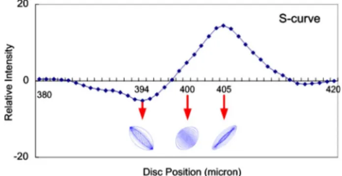
In our system, the optical pickup is designed for a swing-arm actuator共bandwidth of several kilohertz兲, which can be used to maintain the disk continually on focus of the focused beam from the pickup under a feedback mecha-nism. The relative distance between the objective lens and the surface of the disk can be monitored by an astigmatic focus-error detector, which provides such feedback focus error signals共FESs兲. To generate a FES, the DOE is used to focus on a four-quarter photodiode共PD兲, which is 1.5 mm below the DOE, as shown in Fig.1共b兲. Due to the vibration and wobbling of the disk, the objective lens cannot always exactly project its focus spot on the data surface of the disk. In the backward optical path, the focal spot on the PD is therefore moved because of the optical properties of the DOE, as can be seen in Fig.4. In perfect focus, the focal spot is equally distributed on the four segments of the PD with the signal combination共A+C兲−共B+D兲=0. If the disk position is in front of the focal point of the objective lens, the signal combination is 共A+C兲−共B+D兲⬍0. If the disk position is behind the focal point of the objective lens, the signal combination is 共A+C兲−共B+D兲⬎0. The unequal distribution of the spot on the PD generates a curve of FES=共A+C兲−共B+D兲, which is often called the S-curve because of its shape. The curve reflects the position of the disk.
Since our system is finite conjugate, the light reflected from the disk and collected by the objective lens is conver-gent, whether the disk is farther away from best focus or closer to the lens than the plane of best focus. Therefore, our DOE is an elliptically shaped DOE. A similar DOE has been demonstrated by Leger, Scott, and Veldkamp.10They describe the use of a lenslet array made of diffractive ele-ments that couples together the output of many laser diodes in a linear array. Elliptical DOEs were used to compensate for the astigmatism in the output of the individual diodes. In our design, the DOE possesses convergent and astig-matic function instead of pure astigastig-matic function. The pat-tern is designed by binary optics technology and has the wavefront represented by = ⌺ i=1 n ⌺ j=1 n Aijxiyj, 共1兲
where the coefficients Aijare in units of radians. The linear range of the S-curve is 10 to 14m, according to commer-cial specification. The following steps are used to design the DOE and obtain each coefficient Aij. First, the relative distance between the disk and the objective lens is set to be 400m. Under this condition and the specification shown in Fig. 1共b兲, the position of the astigmatic focus-error de-tector can be determined and the current Aijis 0. Second, because half of the maximum linear range of the S-curve is 7m, the relative distance between the disk and the objec-tive lens is then set to be 393m. The coefficient Aij is optimized to have the returned beam from the disk passing through the DOE and focusing in one direction on the as-tigmatic focus-error detector. In this step, the Aij in the direction, such as A共y兲 in the y direction, can be deter-mined. Third, the relative distance between the disk and the objective lens is then enlarged to be 407m. Using the same method, Aijin a direction such as A共x兲 in the x direc-tion, can be determined. Therefore, the phase polynomial is
= A20共x/rx兲2+ A02共y/ry兲2, 共2兲 where rx and ry are the radius of the DOE in x and y directions, respectively, and A20x2 and A
02y2 serve as the combination of a focusing lens and a cylindrical lens that converges the beam and generates the astigmatism. Many sets of parameters can provide the solutions to Eq. 共2兲. Considering the feasibility of micromachining, the mini-mum linewidth of the DOE pattern has to be larger than 2m. The ZEMAX simulated S-curve matching these re-quirements is shown in Fig.5.
The linear range of the focus error signal 共S-curve兲 is 11m, which is comparable with that of current commer-cial optical pickups. The linear range is from 394 to 405m. But the best focus distance is shifted from the middle value of 399.5m to 398m. This is the in-herent limit of micro-optical pickups, since the distance between the disk and the photodetector is small. With the advantage of using DOEs, a passive assembly can also be utilized for adjusting the relative distance of the photode-tector and DOE, as described in Ref.7.
Fig. 4 Variation of a focal spot and its corresponding S-curve.共a兲
Disk surface is far from the objective lens, FES⬎0. 共b兲 Disk surface is in focus of the objective lens, FES= 0.共c兲 Disk surface is near to the objective lens, FES⬍0.
4 Experimental Results
To demonstrate the function of the DOE, its pattern was etched on a SiN layer of a silicon wafer by standard lithog-raphy processes. It was designed to be a four-phase leveled DOE considering the limit of our etching tool. Two steps of etching was utilized to realize it. Each DOE etching depth were therefore optimized to be around 148 nm for the SiN refractive index= 2.1. The alignment error between the two etching steps was controlled to be within⫾0.25m. After etching the SiN pattern on the front side of the silicon wa-fer, a teflon-made tool was used to protect the front side with a SiN pattern. The back side of the wafer was then bulk-etched until etching stopped at the front SiN film. Fig-ure6shows the captured image of a suspended SiN-based DOE under a microscope. To measure its optical perfor-mance, a setup illustrated as Fig. 7 was used. The wave-length of laser is 650 nm. Lens 1, pinhole, and lens 2 are used to provide the convergent beam, of which the conver-gence is equivalent to the case in the designed micropickup. Since the resolution of the image is over the limit of the charge-coupled device 共CCD兲, a 10⫻ image expander is added. The measurement images are shown in Figs. 8共a兲–8共e兲. Each image is equivalent to the case of the dis-tance between the objective lens and the disk being 394m 关Fig. 8共a兲兴, 396m 关Fig. 8共b兲兴, 398.5m 关Fig. 8共c兲兴, 402m关Fig.8共d兲兴, and 405m关Fig.8共e兲兴. We also measured the diffraction efficiency, which was about 68% and lower than the theoretical value of 81%. The difference can be attributed to the misalignment between the two etch-ing steps, the error of etchetch-ing depth, and the absorption and roughness of the SiN layer. Although the measured value is not high, the image of the spot is normally distributed and no severe aberration appears.
5 Conclusion
A micropickup design for small form factor optical drives is presented. Among the optical elements, the function, de-sign procedure, and fabrication of the key element DOE is proposed. By using a DOE assisted by a 45-deg upward beamsplitter, the optical configuration is efficiently simpli-fied without sacrificing much efficiency. The number of components is also reduced. The experimental result of the DOE is satisfactory with a spot image approaching the simulation. An embodied system based on this feasible de-sign concept will be implemented hereafter. Furthermore, we hope that this design has the potential to be applied to a portable storage system of small form factor in the future. Acknowledgments
This work is supported by the Ministry of Economic Af-fairs under grant number 93-EC-17-A-07-S1-0011. References
1. S. Kim et al., “PCMCIA like ultra small form factor optical drive,”
Tech. Dig. Opt. Data Storage 2003, 5–7共2003兲.
2. J. Lee et al., “Design and analysis of small swing arm type optical pickup for small form factor optical drive,” Tech. Dig. Opt. Data
Storage 2004, 147–149共2004兲.
3. I. H. Choi et al., “Miniature optical drives for mobile application,”
Tech. Dig. Opt. Data Storage 2004, 201–203共2004兲.
4. S. C. Kim, Y. S. Kim, S. H. Leea, M. H. Leeb, and J. Y. Kimb, “Ultra small optical pickup module,”Proc. SPIE5069, 335–340共2003兲
5. Y. Chiu, C. H. Chen, J. C. Chiou, W. Fang, and H. P. D. Shieh, “MEMS-based miniature optical pickup,”IEEE Trans. Magn.41共2兲,
967–970共2005兲.
6. S. M. Kang, J. E. Lee, W. C. Kim, N. C. Park, Y. P. Park, E. H. Cho, J. S. Sohn, and S. D. Suh, “Development of integrated mall-form-factor optical pickup with blue-ray disc specification,”Jpn. J. Appl. Phys., Part 145共8兲, 6723–6729 共2006兲.
7. H. F. Shih, C. L. Chang, K. J. Lee, and C. S. Chang, “Design of optical head with holographic optical element for small form factor drive systems,”IEEE Trans. Magn.41共2兲, 1058–1060 共2005兲.
8. L. Y. Lin, J. L. Shen, S. S. Lee, and M. C. Wu, “Realization of novel monolithic free-space optical disk pickup heads by surface microma-chining,”Opt. Lett.21共2兲, 155–157 共1996兲.
9. J. Y. Chang, C. M. Wang, C. C. Lee, H. F. Shih, and M. L. Wu, “Free space optical pickup head with stacked si-based phase element,”
IEEE Photonics Technol. Lett.17, 214–216共2005兲.
10. J. R. Leger, M. L. Scott, and W. B. Veldkamp, “Coherent addition of AlGaAs laser arrays using microlenses and diffractive coupling,”
Proc. SPIE 884, 82–89共1988兲.
Chi-Hung Lee graduated from the
Depart-ment of Materials Science and Engineering, National Cheng Kung University, in 1995, and received his master’s degree there in 1997. Since 2002, he has been with the Flat Panel Display System Laboratory, Depart-ment of Photonics and Institute of Elec-trooptical Engineering, National Chiao Tung University. His research interests include optical storage, diffractive optical elements, and microfabrication.
(a) (b) (c) (d) (e)
Fig. 8 Measured images from the suspended four-phase leveled
DOE.
Fig. 6 Photograph of the four-phase leveled DOE.
Fig. 7 Schematic illustration of the optical measurement system for
Yi Chiu is a professor in the Department of Electrical and Control
Engineering, National Chiao Tung University. He received his BS in electrical engineering from National Taiwan University in 1988, his MS in electrical and computer engineering from Carnegie Mellon University in 1991, and his PhD in electrical and computer engineer-ing from Carnegie Mellon University in 1996. He was a manager at Acer Media Technology Incorporated. His research interests include optical storage, integrated near-field optical heads for hybrid record-ing, MEMS-based electrostatic vibration-to-electric energy convert-ers, and photonic systems on chips.
Han-Ping D. Shieh received his BS degree from National Taiwan
University in 1975, and his PhD in electrical and computer engineer-ing from Carnegie Mellon University, Pittsburgh, Pennsylvania, in 1987. He joined National Chiao Tung University共NCTU兲 in Hsinchu, Taiwan, as a professor at the Institute of Opto-Electronic Engineer-ing and the Microelectronics and Information Research Center 共MIRC兲 in 1992, after having been a research staff member at IBM T.J. Watson Research Center, Yorktown Heights, New York since 1988. He now is the AU Optronics Chair professor and associate director at MIRC, NCTU. He founded the Display Institute at NCTU in 2003, the first such graduate academic institute in the world dedi-cated to display education and research. He also has held a joint appointment as a research fellow at the Center for Applied Sciences and Engineering, Academia Sinica, since 1999. His current research interests are in display, optical MEMS, nano-optical components, and optical data storage technologies.