Received March 11, 1997; accepted December 16, 1997. Communicated by Jang-Ping Sheu.
* This research was supported in part by the National Science Council, R.O.C. under Grant NSC 85-2213-E-009-120. The valuable comments of the reviewers have significantly improved the quality of the paper.
521
Design and Implementation of a Fault
Tolerant ATM Switch
*KUOCHEN WANGAND FENG-MING LIN Department of Computer and Information Science
National Chiao Tung University Hsinchu, Taiwan 300, R.O.C. E-mail: [email protected]
In this paper, we propose a new method to build a fault tolerant ATM switch. Using this method, we can build an ATM switch which has two disjoint paths between each input/ output pair. The key component in the proposed switch is a 2 ¥ 2 FTSE (Fault Tolerant Switching Element), which can be used as the basic building block for high speed ATM switches. The design of the FTSE-based fault tolerant ATM switch is based on a multi-path, self-routing principle. In terms of modularity, the proposed FTSE is suitable for building any multistage interconnection network (MINs). Thus, we can construct an MIN which has two levels of fault tolerance ability, and in which the redundant paths are in proportion to the network size. From the results of mathematical analysis, we conclude that our ATM switch uses fewer switching elements and has more redundant paths than other comparable ATM switches. The ATM switch is described using VHDL. By means of VHDL simulation, we verify the functionality of the switch. We have also synthesized the ATM switch to evaluate its delay and area. The experimental results demonstrate that the reliability/cost ratio of the fault tolerant FTSE-based ATM switch is better than those of other comparable switches.
Keywords: ATM switch, broadband ISDN, fault tolerance, fault tolerant switching element, multistage interconnection network, redundant path
1. INTRODUCTION
Asynchronous Transfer Mode (ATM) was developed for use in Broadband Integrated Service Digital Networks (B-ISDN). B-ISDN is designed to meet the needs of future appli-cations (data, voice, image and video, etc.). There are economies of scale in having a single network to provide all telecommunications and data services [1]. It goes without saying that B-ISDN will play a significant role in future networks. Since ATM is the core data transmission technique for B-ISDN, we need high speed switches for fast switching. Un-der ATM transmission, no matter what kind of data is transmitted, the transmitted data is chopped into basic data transmission units of 53 bytes. The basic data unit is called a cell. The 5 bytes at the beginning of the cell is the cell header. The functions of the cell header include routing, cell priority, and HEC (Header Error Control). The remaining 48 bytes are
reserved for user data. For switching cell streams, several ATM switch architectures have been proposed. An MIN architecture is considered a better way to transmit ATM cells in terms of the balance between hardware cost and switching speed.
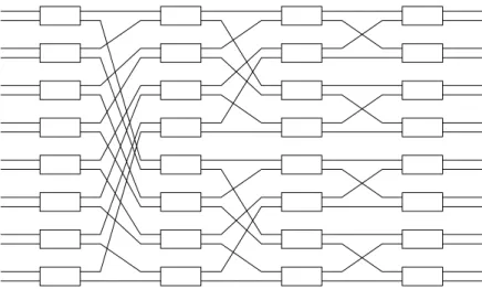
There are several MIN architectures suitable for ATM switches, such as Banyan, Baseline, Omega, and Benes [2]. Most of them are a variation of the Banyan switch. The configuration of a 16 ¥ 16 Baseline switch is shown in Fig. 1. The advantage of MINs for ATM switches is their parallel processing capability. For example, an N ¥ N MIN can process N independent cells simultaneously. Under parallel processing, it is possible that two independent cells will contend for a link or a switching element (SE) output port within an MIN. This situation is called blocking or contention. Such MIN switches, called block-ing switches, include, Banyan, Baseline, and Omega. The method for resolvblock-ing contention is to add queues to buffer the low priority cells in contention or to provide multiple paths between each input/output pair such as in the Benes switch [2]. In this switch, the number of multiple paths and the number of stages are in proportion to the size of the switch. However, its switch size and stage number are nearly double those of the Banyan switch. Furthermore, it also needs a complex routing algorithm between each input/output pair. Contention can also be solved by rearranging the paths that have been set up already. There are some switches that are non-blocking. Batcher-Banyan [3, 4] is one of them. It used a switch called Batcher [4] to sort incoming cells in a certain order in front of the Banyan switch in order to avoid internal blocking. Hence, the Batcher-Banyan switch can avoid internal blocking without using any buffers. Normally, the Batcher switch is more compli-cated and larger than the Banyan switch. This means that we need to pay a high hardware cost to resolve the internal blocking problem.
Several ATM switch architectures were presented in [5-14] to satisfy the high speed switching requirement. We can classify them into two categories: with fault tolerance or without. A switch architecture without fault tolerance concentrates on making the switch-ing rate as fast as possible. Owswitch-ing to no fault tolerance, if a fault occurs in a switch, the switch will be partially or totally disrupted. A few papers have dealt with fault tolerant ATM switch designs [7-10, 13]. These approaches are based on a 2 ¥ 2 modified SE but add extra SEs [7] or links [9], or use multiple-pass [10] to provide fault tolerance. In [9], a modified Delta network which provides fault tolerance was presented. One extra stage and double links were added to the original Delta network. Thus, a 2 ¥ 2 SE was replaced by a 4 ¥ 4 SE in the middle stage of the resulting network and a 4 ¥ 2 SE in the last stage, respectively. In [7], some subswitches were used to enhance the fault tolerance of the conventional multistage interconnection network by providing alternative paths between each input/output pair. The larger the switch size is, the greater the number of redundant paths it has. However, the basic building block, i.e., the SE, is more complicated than the conventional one. The number of SEs is almost twice that of the Benes network. Also, the SEs in the switch are of different sizes. The added SEs also make a decision in selecting a path more complicated. A modified SE called PHOENIX [8] is a 2 ¥ 2 SE. PHOENIX is based on a 2 ¥ 2 crosspoint buffered SE. The characteristics of PHOENIX allow it to be constructed as a multiplexer or demultiplexer. We can build a larger ATM switch using PHOENIX only. PHOENIX employs several queues to buffer contention cells. The com-plex scheme in PHOENIX initiates an adaptive routing or triggers an alternative switch fabric when a fault occurs. As to the multiple-pass method, the cell is rerouted by the faulty switch several times, if necessary, in order to reach the proper destination [10]. However, allowing a cell to traverse the switch several times will cause some input port to be occu-pied and will increase the switching time needed for a cell to reach its destination.
The SE we will present here is a 2 ¥ 2 FTSE (Fault Tolerant Switching Element) which can be the basic building block of an MIN switch for high speed broadband networks. Since the fault tolerance capability is quite important in a high speed network, the proposed FTSE can satisfy this need. The fault tolerance scheme in the FTSE employs one spare IC and two spare OCs to provide multiple paths between each IC/OC pair. This enables the FTSE to tolerate faults. We also propose a method to build an MIN switch using the FTSE as the basic building block. The proposed method provides the switch with two disjoint paths between each input/output pair. Since the resulting MIN as well as the FTSE both have the capability of fault tolerance, our switch has two levels of fault tolerance. In other words, the resulting switch can tolerate more faults within the switch. We use the IEEE Standard, VHDL (VHSIC Hardware Description Language), to describe the ATM switch. VHDL simulation has been used to verify the correctness of the functionality of the switch. VHDL synthesis has also been used to analyze the delay time and area of the switch to make sure that it meets the speed requirement of the ATM switch with low overhead.
The organization of this paper is as follows. In the next section, we describe the FTSE and a method to build an FTSE-based MIN. In section 3, we give an example to demonstrate how to route a cell in the resulting MIN. In section 4, we analyze the hardware complexity and the redundant paths of the proposed switch and give a comparison with other switches. In section 5, we evaluate and compare the reliability and cost effectiveness of our switch compared with other switches. In section 6, we describe the proposed ATM
switch using VHDL [15-17]. The VHDL simulation and synthesis results help us validate the switch design and analyze the delay time encountered as well as the area of the pro-posed switch. Finally, we give some concluding remarks in section 7.
2. DESIGN APPROACH
There are two ways to ensure that an entire network works properly. One way fo-cuses on the switching network itself while the other fofo-cuses on the SE. The method in [18] focuses on the fault tolerant design of the network itself. It groups several physical links into multilinks. If a physical link within the multilinks fails, a cell will be rerouted by the remaining physical links. This will cause the remaining physical links to have a higher load. In order to enable the traffic to be evenly dispatched at every switch in the network, we focus on the fault tolerant designs of the SE as well as the switching network.
2.1 The Architecture of the FTSE and Its Functions
The configuration of the proposed 2 ¥ 2 FTSE is shown in Fig. 2. The FTSE is composed of the following basic parts : two ICs (Input Controllers), a spare IC, a selector, two OCs (Output Controllers), two spare OCs, two MUXs (multiplexers), and a BFS_CTRL (backward fault signal controller). Next, we will describe each part of the FTSE.
l Logic Routing demux IC 1 IC2 demux BFS_CTRL OC OC 1 2 2 MUX Selector MUX 1 2 1 spare IC spare OC spare OC BFS u BFS
∑ ICs (Input Controllers) and spare IC
The two ICs are the inlets of the FTSE. The spare IC is used for fault tolerance. When either the normal IC1or IC2 is faulty, then the spare IC begins to work by controlling the
corresponding demultiplexer (demux). A demultiplexer is a simple device and can be designed so as to be very reliable. There is a buffer of size one in the spare IC. If both
IC1and IC2 are broken, the low priority cell will be buffered in the buffer of the spare IC, Fig. 2. The configuration of the proposed 2 ¥ 2 FTSE.
and the high priority cell will be passed to the selector via the spare IC. The ICs and spare IC will report their status to BFS_CTRL to help BFS_CTRL determine the current state of the FTSE.
∑ Selector
The next stop for incoming cells is a 3 ¥ 2 selector. The task of the selector is to select two incoming cells from three incoming cells. Control signals coming from the ICs and the spare IC activate the selector in order to make a proper selection among the three incom-ing cells.
∑ Routing Logic
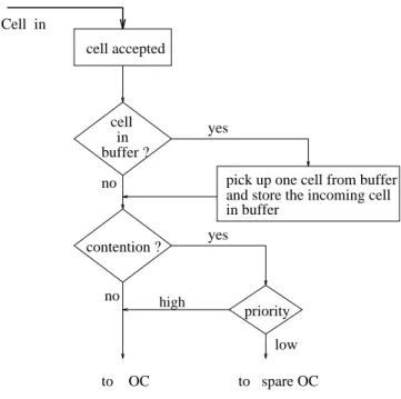
The routing logic first checks whether or not there are cells in the two shared buffers. If there are cells in the shared buffers, then the first incoming cell will be picked up and sent to the desired OC or spare OC. However, if the two shared buffers are empty, the incom-ing cell will be sent to its desired OC accordincom-ing to the i-th bit of the routincom-ing tag. Depend-ing on the number of stages in the network, the routDepend-ing tag will be inserted by the interface before each cell enters the switch. Again, a spare OC is used when faults occur in the corresponding OC. Under normal conditions, if there is no fault and the two shared buff-ers are empty, the two OCs and two spare OCs will still be filled with cells when output contention occurs. Otherwise, one of the contention cells (low priority) will be buffered in the shared buffers. The operation algorithm of the routing logic with consideration of faults is given in Fig. 3. Since two shared buffers will give better performance in terms of buffer use than two dedicated buffers, we use two shared buffers in our buffer technique. These two shared buffers are FIFO queues. Since we have two shared buffers, contention cells are buffered in the upper buffer first. If the upper buffer is full, then the lower buffer will begin to buffer the remaining contention cells. In order to maintain the proper cell sequence, if the lower buffer begins to buffer contention cells, it will keep buffering until it is full. The routing logic will take cells from the upper buffer first and then from the lower buffer. However, no matter which buffer is currently being fetched, it will continue fetching until the buffer is empty. One possibility is that many cells may contend for the same output port, causing the two shared buffers to fill up. When this scenario happens, cell loss will occur.
∑ OCs (Output Controllers) and spare OC
If a cell passes through the routing logic successfully, the next stop in the FTSE is OC1, OC2, the spare OC1 or the spare OC2. If faults occur in OC1 or OC2 (the spare OC1 or the
spare OC2), the cell can only be sent to the spare OC1 or the spare OC2 (OC1 or OC2). Like
the ICs and the spare IC, the OCs and the spare OCs will report their status to BFS_CTRL.
∑ MUX (Multiplexer)
When a cell reaches OC1, OC2, the spare OC1, or the spare OC2, the corresponding MUX
(multiplexer MUX1 or MUX2) selects one of the cells from them. Since the high priority
cell is in OC1 or OC2, the MUX will select a cell from OC1 or OC2 first. In other words, the
MUX is designed to select from OC1 or OC2 first and then the spare OC1 or spare OC2.
Fig. 3. The operating algorithm of the Routing Logic. high low priority cell accepted yes yes Cell in in cell buffer ? contention ? no to spare OC no to OC
pick up one cell from buffer in buffer
and store the incoming cell
yes yes cell accepted in Cell in cell buffer ? contention ?
no pick up one cell from buffer
in buffer
and store the incoming cell
no high
low priority
to OC (spare OC) store in buffer
(a) The operation of routing logic without faults.
∑ BFS_CTRL (Backward Fault Signal Controller)
The function of the BFS_CTRL is to determine the state of the FTSE [19]. It will receive the BFS signals (BFSu and BFSl) of the FTSE in the next stage. If any BFS signal is set true, then the corresponding current BFS signal will also be set to true. Otherwise, it will check the state of the current FTSE and set the BFS signals to a proper value. The state of the current FTSE is based on the status of the ICs, spare IC, OCs and spare OCs. If IC1
and the spare IC or OC1 and the spare OC1 are both faulty, then BFSu is set to true. Similarly, if IC2 and the spare IC or OC2 and the spare OC2 are both faulty, then BFSl will be set to true. BFSu and BFSl signals will help the interface, which is at the front of the switch, generate a proper routing tag.
According to the design described above, there are two paths from an IC to the selec-tor and two paths from the routing logic to an MUX. Therefore, there are 4 paths between each IC/OC pair. In an IC fault, a cell can enter via a spare IC. In an OC fault, a cell can still go through a spare OC. The spare OCs can also help eliminate contention at the same output port. When contention occurs, high priority cells pass through the normal OC and low priority cells are buffered in the spare OC.
2.2 An ATM Switch Built by FTSEs
Since the size of the proposed FTSE is 2 ¥ 2, we need a method to enlarge it, such as to 4 ¥ 4, 8 ¥ 8, 16 ¥ 16, etc. Here, we propose a method to build an MIN using the FTSE as a basic building block. An MIN built using FTSEs is called an FTSE-based network. An MIN is a better way to satisfy the needs of ATM switching in terms of hardware cost and switching speed. Some MINs like Baseline, Banyan, Omega, etc., have only one unique path between each input/output pair. Therefore, these switches lack fault tolerance. The fault tolerant MIN we introduce here is based on the Baseline network (see Fig. 1). We add one extra stage to the Baseline network. There are N/2 FTSEs in each stage of an N ¥ N FTSE-based switch. The extra stage can be appended to the first or to the last stage of the Baseline network. As depicted in [20], a general method is used to insert e stages (to the back) and p planes into the logN network. In this paper, we will only discuss the situation where an extra stage is appended to the first stage of the Baseline network. The discussion would be similar if we appended an extra stage to the last stage of the Baseline network. To build a 4 ¥ 4 MIN, we append 2 FTSEs to the first stage of the 4 ¥ 4 Baseline network. Before we discuss how to build an ATM switch using FTSEs, we will define two terms first. Since an ATM switch built using FTSEs has two disjoint paths, as shown in Fig. 4(a), we call the path that passes through plain FTSEs a normal path. Otherwise, if a path passes through at least one hatched FTSE, we call the path a hatched path. Thus, each incoming cell can reach its desired output by passing through either paths of the MIN. For an 8 ¥ 8 MIN, we add 4 FTSEs to the first stage of the 8 ¥ 8 Baseline network. As shown in Fig. 4 (b), there also are two disjoint paths: one is a normal path and the other is a hatched path. In a similar fashion, we can construct an MIN of any size.
The resulting FTSE-based ATM switch inherits the self-routing property of the Baseline switch. The major difference, in comparison with the Baseline switch, is that it has two disjoint paths between each input/output pair. Under normal conditions, the normal path 3 between each input/output pair is selected. The hatched path is used when the switch de-tects faults in the normal path. Using the proposed method, we can build a fault tolerant ATM switch of any size using the FTSE only.
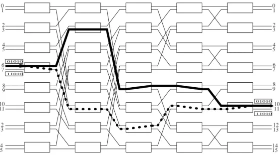
Fig. 5. A routing example for the proposed 16 ¥ 16 MIN.
Fig. 4. The construction of two MINs using FTSEs.
01010 11010 01010 11010 0 1 2 3 4 5 6 7 8 9 10 11 12 13 14 15 0 1 2 3 4 5 6 7 8 9 10 11 12 13 14 15 0 1 2 3 0 1 2 3 0 1 2 3 5 4 6 7 0 1 2 3 5 4 6 7
(a) A4 x 4 MIN built by 2 x 2 FTSE.
3. ROUTING IN THE ATM SWITCH
3.1 Singlecast Routing
Since our fault tolerant ATM switch has two-level redundant paths, a routing path is selected based on the two levels: one is in the FTSE and the other is in the resulting MIN. There are 4 paths between each IC/OC pair in the FTSE. Under normal operations, (i.e., there is no fault and the shared buffer is empty), a cell will be sent to a selected OC. The routing scheme for the proposed FTSE-based ATM switch is similar to that of the Baseline switch, except that our switch needs extra control for the first stage. Under no fault conditions, the routing bit for the first stage is “0”. Otherwise, the routing bit for the first stage is “1” if a fault occurs in the normal path. Assume that d1, d2, d3, ..., dn is the binary representation of the destination address for the proposed N ¥ N ATM switch, where n = log2N +1. Each
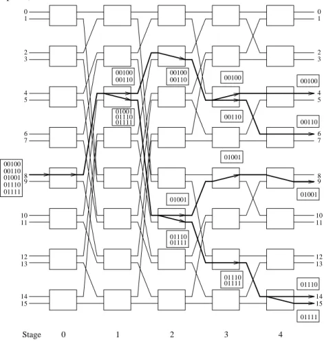
FTSE simply checks the corresponding bit of the destination address. For instance, the FTSE at the i-th stage checks the i-th bit and directs the cell to the upper half of the FTSE or the lower half of the FTSE according to the value of the i-th bit, which is either “0” or “1”, respectively. For example, given a 16 ¥ 16 ATM switch, assume that input port 6 has one cell destined for output port 10. The binary address of output port 10 is “1010”. In the fault-free (fault) situation, a “0” (“1”) bit will be inserted at the left end of the binary address. Thus, the extented routing address is “01010” (“11010”). However, if contention occurs, the contention cell with low priority will be buffered in the shared buffers. In this way, no internal blocking will occur. The final routing paths for the 16 ¥ 16 ATM switch are depicted in Fig. 5. There are two disjoint routing paths shown in Fig. 5. One is the routing path with no faults (solid line) and the other is the routing path with faults (dashed line).
3.2 Broadcast and Multicast Routing
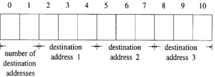
The routing method in an N ¥ N FTSE-based network can be further modified to meet broadcast and multicast needs. The cell format for broadcast and multicast routing is differ-ent from that of normal point-to-point routing. The cell format for broadcast and multicast is shown in Fig. 6. The broadcast bit indicates whether the cell should be broadcast or not. The multicast bit is set if the cell is to be multicast. If the multicast bit is set, the following field is used to specify the number of destination addresses and the destination addresses of the multicast cell. In order to maintain the self-routing property of the Baseline network, we adopt the explicit addressing scheme [21]. Fig. 7 illustrates the format of the destination addresses of a 4 ¥ 4 FTSE-based network, where the first two bits indicate the number of destination addresses. In this example, the number of destination addresses is 3.
Broadcast Routing If a cell has to be broadcast, the broadcast bit is set to “1”. In each
stage, except for the first stage, the routing logic will replicate and send this cell to the upper and lower OCs within each FTSE if the broadcast bit is set. Fig. 8 shows the broad-cast routing arrangement in a 16 ¥ 16 FTSE-based ATM network.
Multicast Routing If a cell has to be multicast, the multicast bit is set to “1”. In each stage,
a cell is selectively replicated and sent by the routing logic to the upper, lower, or both OCs in an FTSE according to the destination addresses. Let the stage number of an N ¥ N
Fig. 8. The broadcast routing arrangement in a 16 ¥ 16 FTSE-based ATM network. 9 10 11 8 12 13 14 15 7 6 5 4 3 2 1 0 7 6 5 4 3 2 1 0 9 8 10 11 12 13 14 15 cell broadcast
Fig. 7. The destination address format for multicast. Fig. 6. The cell format for broadcast and multicast.
cell ATM bit multicast broadcast bit destination addresses
Fig. 9. The multicast routing arrangement in a 16 ¥ 16 FTSE-based ATM network. 01110 9 10 11 8 12 13 14 15 7 6 5 4 3 2 1 0 7 6 5 4 3 2 1 0 9 8 01001 00110 00100 00110 00100 00110 00100 00100 00110 01111 01001 01111 01110 01111 01110 01001 10 11 12 13 14 15 Stage 0 1 2 3 4 00100 00110 01001 01110 01111 01001 01110 01111
FTSE-based network be from 0 to log2N. Under normal operations, assume that a cell from
inlet 8 has to be multicast to outlets 4, 6, 9, 14 and 15 in a 16 ¥ 16 FTSE-based ATM network, where N = 16, as shown in Fig. 9. The binary representations of destiation ad-dresses 4, 6, 9, 14 and 15 are “00100”, “00110”, “01001”, “01110” and “01111”, respectively. “0” is appended to the left end of each destination address for normal operations. In each stage, the FTSE first checks the multicast bit and then the destination addresses. In stage 0, since the first bits of all the destination addresses are all “0”, the cell is sent to the upper OC without replication. In stage 1, the second bits of the destination addresses contain “0” and “1”, so the cell is copied and sent to the upper OC and lower OC, respectively. In the subsequent stages, each FTSE repeats the same procedure described above until the cells reach the last stage.
4. COMPARISON WITH OTHER FAULT TOLERANT ATM SWITCHES The comparison criteria are based on hardware complexity (expressed in terms of the number of SEs) and fault tolerance capability (expressed in terms of the number of redun-dant paths).
4.1 Hardware Complexity
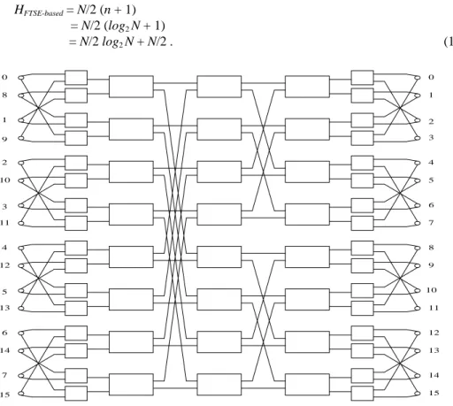
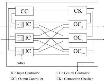
In [13], a basic SE was used to build a fault tolerant MIN. Since they did not show the structure of the basic SE, we can not compare our proposed FTSE with their SE. Hence, we can only compare the FTSE-based switch with the MD-Omega network [8], as shown in Fig. 10, and Itoh’s network [7], as shown in Fig. 11. For the purpose of comparison, we also show the SEs of these two networks. Fig. 12 shows the basic PHOENIX SE of the MD-Omega network [22], and Fig. 13 shows the basic SE of Itoh’s network [7]. The self-checking checker in PHOENIX corresponds to our routing logic and BFS_CTRL, while CC and CK in the SE of Itoh’s network corresponds to our routing logic and BFS_CTRL. Therefore, we can see that the SEs of both networks are comparable to our proposed FTSE. We know that there are n +1 stages in our FTSE-based ATM switch. Therefore, we can calculate the number of FTSEs needed in an N ¥ N MIN. Since there are N/2 FTSEs in each stage, the total number of FTSEs required is
HFTSE-based = N/2 (n + 1) = N/2 (log2 N + 1)
= N/2 log2 N + N/2 . (1)
Fig. 10. The 16 ¥ 16 MD-Omega network. 4 12 5 13 6 14 7 15 0 8 1 9 2 10 3 11 15 14 13 12 11 10 9 8 7 1 0 6 5 4 3 2
Fig. 12. The PHOENIX switching element in the MD-Omega network.
Fault Input
Self-checking Checker
FIFO seq. A00 FIFO seq. A01 FIFO seq. A02 FIFO seq. A03 FIFO seq. A10 FIFO seq. A11 FIFO seq. A12 FIFO seq. A13
1 Output Output 0 1 Input B Sequencer Output Sequencer DcadEnd DcadEnd Fault Input Sequencer A B A Input Sequencer Output 0 FIFO seq. B00 FIFO seq. B01 FIFO seq. B02 FIFO seq. B03 FIFO seq. B10 FIFO seq. B11 FIFO seq. B12 FIFO seq. B13
Fig. 11. Itoh’s 16 ¥ 16 network.
R3 R2 R2 R1 R1 R1 R1 R2 R1 R1 R2 R1 R1 R1 R1 R1 R1 0 1 2 3 4 5 6 7 8 9 10 11 12 13 14 15 0 1 2 3 4 5 6 7 8 9 10 11 12 13 14 15
The number of SEs used by the MD-Omega network and Itoh’s network is N/2 (n - 1) + 2 ¥ N and N (n - 1) + 1, respectively. Table 1 shows the number of SEs used in each network in variance of network size. From Table 1, we conclude that to build the same size
Fig. 13. The switching element of the Itoh’s network.
Fig. 14. Number of SEs used in each 2n¥ 2n MIN.
IC
IC
IC
OC
0OC
1OC
sub IC : Input Controller OC : Output Controller CC : Central Controller CK : Connection CheckerCC
CK
bufferTable 1. The number of SEs used in each network in variance of n (or log2 N).
Network Size (n) 2 3 4 5 6 7 8 9 10
MD-Omaga Network 10 24 56 128 288 576 1408 3072 6656 Itoh’s Network 5 17 49 129 321 769 1793 4097 9217 FTSE-based Network 6 16 40 96 224 512 1152 2560 5632
N ¥ N fault tolerant MIN, our FTSE-based switch requires the fewest SEs. A graphical representation of Table 1 is shown in Fig. 14. This further distinguishes these three networks. Using fewer SEs will make VLSI implementation of a large fault tolerant MIN more feasible.
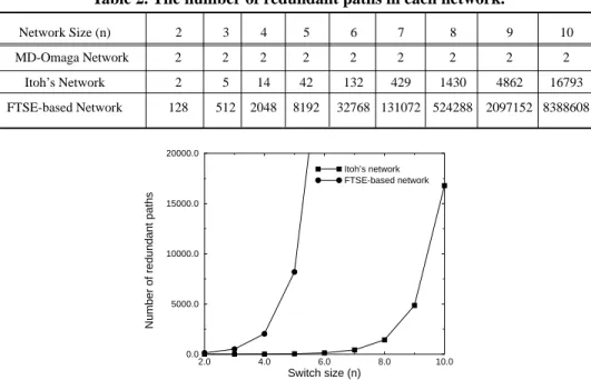
4.2 Redundant Paths
If a switch network can provide more redundant paths, it will be able to survive more faults. We will compare redundant paths among the MD-Omega network, Itoh’s network, and the FTSE-based network. The number of redundant paths in the MD-Omega network built using PHOENIX is 2 regardless of the network size. For each node in Itoh’s network, there are M(i, j) paths to the last node, where (i, j) is the node position. The number of redundant paths of the Itoh’s network (RItoh’s) [7] is expressed as:
M (n, 0) = M (n - 1, 0) + M (n, 1)
M (n, k) = M (n - 1, k - 1) + M (n, k + 1)
M (n, n - 1) = 1. (2)
As mentioned before, there are 4 redundant paths between each IC/OC pair in the FTSE. Therefore, for an N ¥ N FTSE-based switch, the number of redundant number of paths for each input/output pair is
RFTSE_based = (22)(log2 N + 1) ¥ 2
= 22 (log2 N + 1) + 1. (3)
Note that the multiplication of 2 in equation 3 is due to the presence of two disjoint paths for each input/output pair. Table 2 shows that the number of redundant paths in the FTSE-based network is far larger than that of the other two networks of the same size. In Fig.15,
Fig. 15. Number of redundant paths in a 2n ¥ 2n MIN.
2.0 4.0 6.0 8.0 10.0 Switch size (n) 0.0 5000.0 10000.0 15000.0 20000.0 Itoh’s network FTSE-based network
Number of redundant paths
Table 2. The number of redundant paths in each network.
Network Size (n) 2 3 4 5 6 7 8 9 10
MD-Omaga Network 2 2 2 2 2 2 2 2 2
Itoh’s Network 2 5 14 42 132 429 1430 4862 16793
we can see the great increase in the number of redundant paths in the FTSE-based network with respect to the network size. Since the number of redundant paths in the MD-Omega network is a constant 2, we do not include it in Fig. 15.
5. RELIABILITY ANALYSIS
5.1 Fault Model
The fault model discussed in this section is similar to that proposed in [7]. Faults can occur in ICs, spare ICs, OCs, spare OCs and links that connect two adjacent SEs. In our proposed method, the functionality of a spare IC is similar to that of an IC except that it can accept two cells concurrently. Hence, we treat a spare IC as two independent ICs. Similar to [23], the two ICs that connect to the same OC and spare OC in the previous stage com-prise the input module. The OC and the corresponding spare OC comcom-prise the output
module. An element is formed by an input module in the current stage, an output module in
the previous stage, and the links between them. If there are faults in the input module, output module, or links, the element is considered to be faulty. When an element is marked as faulty, then it remains permanently faulty. Since a path is broken when an element is faulty, we take an element as our basic analytical unit. Our analysis is based on the follow-ing assumptions [7]:
∑ Events in which an element becomes faulty are independent and occur randomly. ∑ When there are faults that prevent the connection of an arbitrary input/output pair,
the network is considered to have failed.
Similar to [23], our analysis only concentrates on the elements between the first stage and the last stage of a network.
5.2 The Reliability of the FTSE-based ATM Switch
In an FTSE-based ATM switch, there are two disjoint paths between each input/ output pair. The FTSE-based switch is considered to be faulty if the two disjoint paths are both broken. Thus, for each output port at stage i, two elements can be selected which will connect to stage i + 1 (due to the two disjoint paths). The m FTSEs within a stage can be divided into m/2 subsets of 2 elements. A switching network is faulty if both elements in the same subset are faulty. Thus, in an N ¥ N FTSE-based switching network, there are N/ 2 ¥ log2N subsets. Here, we can calculate the average number of faults, K, that causes
network failure. K is expressed as follows [24] :
K i P i i L = ∑ =2 ( ), (4) where
P(i) = Prob {the network fails due to the i-th fault},
L = N/2 ¥ log2N, the number of subsets in an N ¥ N FTSE-based network. P(i) can be further expressed as:
P(i) = Q(i - 1) ¥ R(i), (5)
where
Q(i - 1) = Prob {there are i - 1 faults in the network and the network does not fail},
R(i) = Prob {a fault that makes the network failΩi-1 faults already exists in the network},
and we have [24],
Q i( − =1) 2i−1× −iL1/i2−L1 (6)
R i( )= −(i 1) / (2L− +i 1). (7)
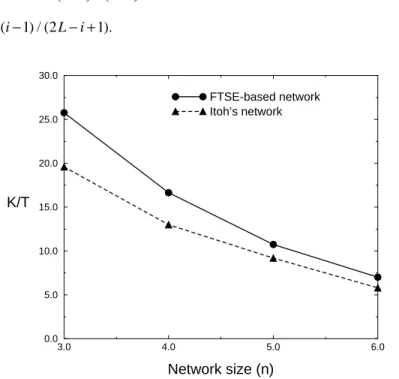
We evaluate the cost effectiveness of an ATM switching network in terms of K/T, where T is the total number of elements in the middle stages of the network. The cost effectiveness of the FTSE-based network and Itoh’s network, respectively, is shown in Fig. 16. From Fig. 16, we can conclude that the cost effectiveness of our FTSE-based network is better than that of Itoh’s network.
Fig. 16. A cost effectiveness comparison between the FTSE-based network and Itoh’s network.
3.0 4.0 5.0 6.0 Network size (n) 0.0 5.0 10.0 15.0 20.0 25.0 30.0 K/T FTSE-based network Itoh’s network
6. SIMULATION AND SYNTHESIS
6.1 VHDL Simulation
According to the design described in section 2, a 4 ¥ 4 FTSE-based ATM switch has been described using VHDL. The design hierarchy of the FTSE-based ATM switch is shown in Fig. 17. Each component of the FTSE was first described. We then wrote a
testbench to verify the functionality of each component. Then, we grouped all the
compo-nents of the FTSE to form a complete 2 ¥ 2 FTSE. Finally, we used the FTSE as a building block to construct an example 4 ¥ 4 FTSE-based ATM switch. The functionality of the 4 ¥ 4 FTSE-based ATM switch has been verified via VHDL simulation.
Fig. 17. The design hierarchy of the FTSE-based ATM switch.
Selector Routing Logic FTSE OC BFS_CTRLSpare OC MUX Spare IC IC Switch ATM 6.2 VHDL Synthesis
The ATM switch described using VHDL can be further synthesized into a gate level representation in a chosen technology. The target technology library we used are lsi_10k, provided by Synopsys. As an example, Fig. 18 shows a schematic view of the FTSE. Based on the synthesis results obtained for the FTSE, we can find that the spare IC has the largest delay. The overall delay for a fault-free FTSE is 5.12 ns. However, the overall delay becomes 5.47 ns when there is a fault in an IC and the spare IC is used. The total area of the FTSE is 58617 (unit area). We can expand the FTSE into a 4 ¥ 4 FTSE-based ATM switch. The overall delay for the 4 ¥ 4 FTSE-based ATM switch is 15.36 ns when it is fault-free and 16.41 ns when a fault occurs in an IC and the spare IC is used. The total area of the 4 ¥ 4 FTSE-based ATM switch is 351702 (unit area). We need two clock cycles to transfer a cell from IC to Routing Logic and a delay time to transfer it from OC to MUX. Thus, the m a x i m u m t h r o u g h p u t o f a 2n ¥ 2n F T S E - b a s e d AT M s w i t c h i s
8 53
2× +× + × +1
( clock cycle time_ _ delay OC( MUX)) (n ).
7. CONCLUSIONS
An ATM switch built using an MIN is inherently a parallel switch since it accepts and processes incoming cells concurrently. This is also the reason why this kind of ATM switch can serve the core switching component for B-ISDN. Our proposed ATM switch is also an
Fig. 18. A schematic view of the FTSE.
MIN. The basic component of our FTSE-based ATM switch is a 2 ¥ 2 FTSE. The FTSE is very flexible and can serve as the basic building block of any kind of MIN. The FTSE not only can process incoming cells quickly, but also has the capability of fault tolerance. We consider faults that may appear in any place within each FTSE and take the necessary actions to overcome such faults. The key feature of the FTSE is the use of a spare IC and two spare OCs. Therefore, it offers multiple paths between each IC/OC pair and makes the ICs and OCs fault tolerant. The problem of cells contending for the same output is resolved by means of shared buffers which store low priority contention cells. Thus, we offer a guarantee service to high priority cells. The method of constructing an MIN using FTSEs provides each input/output pair with two disjoint paths. This two-level of fault tolerance makes our fault tolerant ATM switch more robust. Mathematical analysis shows that our switch is better than other fault tolerant ATM switches in terms of the number of SE used, the number of redundant paths, and the reliability/cost ratio. The VHDL simulation results have verified the functionality of the switch, and the VHDL synthesis results also show that the switch throughput can meet the ATM network requirement.
BFS-DOWN-IN-STATE CLK1 IN-CLK IN-1 IN-2 CLK2 CLK3 CLK4 BFS-UP-IN-STATE LOGIC-0 MM SP-STC2-SEL ROUT PAR-TO-SER PAR-TO-SER PAR-TO-SER PAR-TO-SER MUX F-BIT1 F-GO1 RB-1 BFS-CTRL BFS-DOWN-OUT-STATE BFS-UP-OUT-STATE MUX F-BIT2 F-GO2 RB-2
REFERENCES
1. R. Handel and M. N. Huber, Integrated Broadband Networks, Addision Wesley, 1991. 2. V. E. Benes, Mathematical Theory of Connecting Networks and Telephone Traffic,
Academic Press, New York, 1965.
3. J. Y. Hui and E. Arthurs, “A broadband packet switch for integrated transport,” IEEE
Journal on Selected Areas in Communications, Vol. 5, No. 8, 1987, pp. 1264-1273.
4. K. E. Batcher, “Sorting networks and their applications,” AFIPS Proceedings of Spring
Joint Computer Conference, 1968, pp. 307-314.
5. J. N. Giacopelli, J. J. Hickey, W. S. Marcus, W. D. Sincoskie and M. Littlewood, “Sunshine: a high performance self-routing broadband packet switch architecture,”
IEEE Journal on Selected Areas in Communications, Vol. 9, No. 8, 1991, pp.
1289-1298.
6. Y. S. Yeh, M. G. Hluchyj and A. S. Acampora, “The knockout switch: a simple, modu-lar architecture for high performance packet switching,” IEEE Journal on Selected
Areas in Communications, Vol. 5, No. 8, 1987, pp. 1274-1283.
7. A. Itoh, “A fault tolerant switching network for B-ISDN,” IEEE Journal on Selected
Areas in Communications, Vol. 9, No. 8, 1991, pp. 1218-1226.
8. V. P. Kumar, J. G. Kneuer, D. Pal and B. Brunner, “PHEONIX: a building block for fault tolerant broadband packet switches,” IEEE GLOBECOM’91, 1991, pp. 228-233. 9. W.-S. E. Chen, Y. M. Kim, Y. W .Yao and M. T. Liu, “FDB: a high-performance fault-tolerant switching fabric for ATM switching systems,” IEEE International Pheonix
Conference on Computers and Communications, 1991, pp. 703-709.
10. T. H. Lee and J. J. Chou, “Fault tolerance of banyan using multiple-pass,” IEEE
INFOCOM’92, 1992, pp. 867-875.
11. H. Ahmadi, W. E. Denzel, C. A. Murphy and E. Prot, “A high-performance switch fabric for integrated circuit and packet switching,” IEEE INFOCOM’88, 1988, pp. 9-18.
12. H. S. Kim, “Design and performance of multinet switch: a multistage ATM switch architecture with partially shared buffers,” IEEE/ACM Transactions on Networking, Vol. 2, No. 6, 1994, pp. 571-580.
13. S. W. Seo and T. Y. Feng, “The composite banyan network,” IEEE Transactions on
Parallel and Distributed Systems, Vol. 6, No. 10, 1995, pp. 1043-1054.
14. K. Genda and N. Yamanaka, “TORUS: terabit-per-second ATM switching system ar-chitecture based on distributed internal speed-up ATM switch,” IEEE Journal on
Se-lected Areas in Communications, Vol. 15, No. 5, 1997, pp. 817-829.
15. Z. Navabi, VHDL Analysis and Modeling of Digital Systems, McGRAW-HILL Inc., 1993.
16. S. Mazor and P. Langstraat, A Guide to VHDL, Kluwer Academic Publishers, Norwell, MA, 1993.
17. R. Airiau, J. M. Berge and V. Olive, Circuit Synthesis with VHDL, Kluwer Academic Publishers, 1994.
18. T. V. Landegem, P. Vankwikelberge and H. Vanderstraeten, “A self-healing ATM net-work based on multilink principles,” IEEE Journal on Selected Areas in Communications, Vol. 12, No. 1, 1994, pp. 139-148.
self-routing switch,” IEEE Communications Magazine, Vol. 31, No. 4, 1993, pp. 46-52. 20. D. J. Shyy and C. T. Lea, “Log2(N, m, p) strictly nonblocking networks,” IEEE
Trans-actions on Communications, Vol. 39, No. 10, 1991, pp. 1502-1510.
21. K. E. Law and A. Leon-Garcia, “Multicast and self-routing in ATM radix trees and banyan networks,” IEEE INFOCOM’95, 1995, pp. 951-959.
22. V. P. Kumar and S. J. Wang, “Reliability enhancement by time and space redundancy in multistage interconnection networks,” IEEE Transactions on Reliability, Vol. 40, No. 4, 1991, pp. 461-473.
23. N. Tzeng, P. Yew and C. Zhu, “A fault-tolerant scheme for multistage interconnection networks,” International Symposium on Computer Architecture, 1985, pp. 368-375. 24. L. Ciminiera and A. Serra, “A fault tolerant connecting network for multiprocessor
systems,” International Conference on Parallel Processing, 1982, pp. 113-122.
Kuochen Wang (¤ý°êºÕ ) received the B.S. degree in con-trol engineering from National Chiao Tung University, Taiwan, in 1978, and the M.S. and Ph.D. degrees in electrical engineering from the University of Arizona in 1986 and 1991, respectively. He is currently an associate professor in the Department of Computer and Information Science, National Chiao Tung University. From 1980 to 1984, he worked on network management and on design and implementation of the Toll Trunk Information System at the Directorate General of Telecommunications in Taiwan. He served in the army as a second lieutenant communication platoon leader from 1978 to 1980. His research interests include computer networks, mobile computing and wireless networks, fault-tolerant computing, and computer-aided VLSI design.
Feng-Ming Lin (ªL»ñ»Ê ) received the B.S. degree in infor-mation engineering from Feng Chia University, Taiwan, in 1993 and the M.S. degree in computer and information science from National Chiao Tung University in 1995. Since 1997, he has worked at the Computer Center of National Chengchi University. His re-search interests include fault-tolerant computing, VLSI system design, and interconnection networks.