IEEE TRANSACTIONS ON ELECTRON DEVICES. VOL. 40. NO. 12. DECEMBER 1993 2301
The Effects of H2-02-Plasma Treatment
on the Characteristics of Polysilicon
Thin-Film Transistors
Horng Nan Chern, Chung Len Lee, and Tan Fu Lei
Abstract-The effects of H2-plasma followed by 02-plasma treatment on n-channel polysilicon TFT’s were investigated. It was found that the Hz-02-plasma treatment is more effective in passivating the trap states of polysilicon films than do the Hz- plasma treatment only or the 02-plasma treatment only. Hence, it is more effective in improving the device performance on the subthreshold swing, carrier mobility and the current O N ~ O F F ratio. It is also found that thermal annealing on plasma-treated devices increases the deep states but has no effect on the tail states of the devices.
I . INTRODUCTION
OLYSILICON thin film transistors have been widely
P
used in large-area electronic devices [I]. Recently, they have been studied for applying to higher density SRAM [2]. However, due to the high density of defect states at grain boundaries, polysilicon TFT’s exhibit a poor performance such as a low mobility, a large subthreshold swing, a large threshold voltage and a large leakage current. Many techniques have been investigated to improve the performance of polysilicon TFT’s. One of methods is to reduce the defect states of polysilicon by using the H,-plasma treatment [ 3 ] , [4] to passivate the grain boundaries. It had been found that the characteris- tics of polysilicon TFTs improves after the H2-plasma treatment but the improvement reaches saturation (41, which limits the practical application of the H,-plasma treatment because the performance of hydrogenated poly- silicon TFT’s is still much poorer than that of single-crys- tal Si MOSFET’s. It had also been used to apply the 0,- plasma treatment to polysilicon resistors, but this treat- ment increased grain boundary trap-states and decreased the conductance of polysilicon [SI. However, it was re- ported that the treatment of 02-plasma improved the per- formance of the P-channel polysilicon T F T when the de- vice was succeedingly annealed in an H2/”,
ambient [6]. It had also been reported that a thermal annealing in the O2 or H2+
0, ambient after a passivation layer capping on polysilicon TFT improved the devices performance [6], Manuscript received May 3 , 1993; revised July 2 1, 1993. This work was supported by the National Science Council of R.O.C. under Contract NSC- 81-0404-E009-138. The review of this paper was arranged by Associate Editor J . R. Pfiester.The authors are with the Department of Electronics Engineering and In- stitute of Electronics, National Chiao Tung University, Hsinchu, Taiwan, R.O.C.
IEEE Log Number 9212781.
[7]. Hence, the real role of oxygen in the improvement of polysilicon TFT’s is not understood. It is suspected that the formation of the intergranular oxide within grain boundaries is the main reason to improve the performance since the device with a thermal gate-oxide exhibited a bet- ter performance than those with a deposited gate-oxide In this paper, the effects of H,-plasma followed by 0,- plasma treatment (H2-02-plasma) on polysilicon TFT’s have been studied. It is found that by jointly applying the Hz-plasma and 02-plasma treatments to polysilicon TFT’s, the device performance is better than that with the H,-plasma or the 0,-plasma treatment only. Experimental results also show that the treatment of the O,-plasma did not exhibit the saturation phenomenon as observed in HZ-
plasma-treated devices. Using the method of field effect conductance [SI, it is found that the trap-state density can be effectively reduced by the H2-O2-plasma treatment, es- pecially for the midgap deep-state. The thermal stability of plasma-treated devices was also studied. It is found that the degradation of the device performance after ther- mal annealing is due to the generation of the deep states. 191.
11. EXPERIMENTS
The polysilicon TFT’s studied in this work were pre- pared as follows: Amprphous silicon films of a thickness approximately 1100 A were deposited at 550°C by a low- pressure chemical vapor deposition (LPCVD) system on thermally oxidized silicon wafers. The wafers were then annealed at 550°C for
48
h to transform the deposited amorphous films to polysilicon. The grain size of the re- crystallized polysilicon was about 0.25 pm as observed by using a transmission electron mkroscope (TEM). After defining the active islands, a 690A gat: oxide was grown in dry 0, at 1000°C. Another 3500 A polysilicon film was then deposited at 625°C by the LPCVD system to be the gate electrode. After defining the gate geometry, a self-aligned phosphorus implantation of a dose of 5 X lOI5cm-2 was performed to form the source, drain and gate electrodes. The dopants were activated at 900°C for 30 min in an N, atmosphere. Some samples were subjected to the H 2 / N 2 or/and the O2 plasma treatment. This was done in a commercial 13.5 M Hz parallel-plate plasma reactor at 300°C with a power density of 0.7 W/cm2. 0018-9383/93$03.00 G 1993 IEEE
IEEE TRANSACTIONS ON ELECTRON DEVICES, VOL. 40, NO. 12, DECEMBER 1993 2302
50 Then, all devices were covered with a 5000
A
plasma-enhanced chemical vapor deposition (PECVD) S O 2 for passivation. Contact holes were opened, and A1 was de- posited and then patterned. In order to study the thermal stability of plasma-treated devices, some of the devices were annealed at 400°C for 30 min in an N2 ambient.
The I-I/ characteristics of fabricated devices were mea- sured by an HP4 145B semiconductor parameter analyzer, and the device parameters: the threshold voltage ( Vth), the subthreshold swing (S) and the field effect mobility ( p ) ,
were measured at V, = 0.1 V . The threshold voltage is defined from the intercept on the voltage axis of the straight line in the drain current Id versus the gate voltage
Vg plot. The leakage current IoR is the minimum value of the drain current at V, = 5 V. Using the linearly fitting of the In ( I d ) versus the 1 / k
-
Tplot, where k is the Boltz- mann constant and T is the temperature, the activation energy E,, of the drain current at different gate bias was deduced.-
111. RESULTS AND DISCUSSIONS
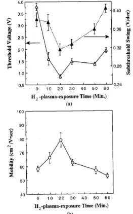
The I- V characteristics of n-channel polysilicon TFTs with a 60 min H2-plasma, a 50 min H,-plasma followed by a 10 min 02-plasma, a 20 min H2-plasma followed by a 40 min 02-plasma and 60 min 02-plasma treatments are shown in Fig. 1. The I-V curve of the device without the plasma treatment is also shown for comparison. It is seen that the Ho2-02-plasma treatment had a better improve- ment effect on the devices than did the H2-plasma treat- ment only or the 02-plasma treatment only. It was per- formed on experiment by applying TFT devices the H2- 02-plasma for a total 60 min but varying the H2- plasma exposure time from 0 to 60 min and measuring the change of the threshold voltage, the subthreshold, and the electron mobility of the devices. The results are shown in Fig. 2 in terms of the H2-plasma exposure time. The ex- perimental result revealed that all the devices with the H2- plasma treatment followed by 02-plasma treatment exhib- ited a better performance than those with the H2-plasma treatment only or the 02-plasma treatment only, and the device treated with a 20 min H2-plasma followed by a 40 min 02-plasma exhibited the best performance.
In order to obtain a clearer picture on the passivation effect of the H2-02-plasma treatment, devices with the H2-plasma treatment only and the 0,-plasma treatment only were also studied systematically. Fig. 3(a) and (b) show the change of the subthreshold swing and the elec- tron mobility respectively of the devices with H2-plasma treatment only and 0,-plasma treatment only as a function of the plasma-exposure time. It is found that the improve- ment of the H2-plasma treatment on the devices saturates after a 50 min plasma treatment and further increasing the H2-plasma-exposure time does not significantly improve the device. For 02-plasma-treated devices, the perfor- mance improves with the plasma-exposure time up to 120 min. The mechanism for the saturated passivation phe- nomenon of H2-plasma treatment might be due to that the
-
60 mi" H,-plasma- 5 0 5 1 0 15
Gate Voltage (V)
Fig. 1 . l d - V x characteristics at Vd = 5 V of polysilicon TFT's with a 60
min H,-plasma, a 50 min H,-plasma followed by a 10 min 0,-plasma, a
20 min H,-plasma followed by a 40 min 0,-plasma and a 60 min 0,-plasma treatment respectively. The I - V curve of the device without plasma treat- ment is also shown for comparison. All devices had a W / L = 40 fim/lO
pm.
4.0 I I
0.24
0.5' I ' " " "
0 10 2 0 30 40 5 0 6 0
H , -plasma-exposure Time (Min.) (a)
loo 90
1
H,-plasma-exposure Time (Min.)
(b)
Fig. 2. (a) The threshold voltage and the subthreshold swing; and (b) the electron mobility for the H,-0,-plasma-treated devices as a function of the H,-plasma-exposure time. The total plasma-exposure time was 60 min. grain boundaries act as hydrogen traps rather than diffu-
sion paths [lo]. After hydrogen atoms are trapped at the
grain boundary, further H diffusions are impeded. Hence, the hydrogen passivation of grain boundaries in polysili-
CHERN et al. : EFFECTS OF HI-02-PLASMA TREATMENT ON THIN-FILM TRANSISTORS ~ 60 min H2 plasma+ 60 min 0 2 plasma -0- H2plasma -.t- 02piasma o,290 0.2' " " " " " " 0 2 0 4 0 6 0 8 0 100 1 2 0
Plasma-exposure Time
win)
(a)7
-U- H2 plasma+
0 2 piasma 1 0 T ' ' " " " " " 0 20 4 0 6 0 8 0 1 0 0 1 2 0Plasma-exposure Time win)
(b)
Fig. 3. (a) The subthreshold voltage; and (b) the electron mobility for the H,-plasma-treated and the 0,-plasma-treated devices as a function of the plasma-exposure time.
con TFT's is saturated after a period of H2-plasma treat- ment. From Fig. 3 , the initial passivation rate is higher for the H2-plasma treatment, while for the long plasma- exposure time (
>
60 min), the 02-plasma-treated devices exhibit higher electron mobility than do the H2-plasma- treated devices. In a previous work [6], it was report that 02-plasma treatment can enhance the hydrogen effect to reduce the dangling bonds in the succeeding H,/N2 an- nealing step. However, our 02-plasma-treated devices which were not annealed in an H2/N2 ambient also show the passivation effect. Hence, the passivation effect of the 02-plasma treatment is caused by oxygen atoms them- selves. It is believed that oxygen in polysilicon tends to segregate to grain boundaries and forms silicon-oxygen bondings [l 11. If the concentration of oxygen in polysil- icon is not high, the formation of silicon-oxygen bonding reduces the density of Si dangling bond, thereby reduces the density of trap states and the barrier potential [9]. The slower passivation rate of the 02-plasma may be due to that the diffusivity of oxygen atoms in polysilicon is smaller than that of hydrogen atoms at 300°C.From the above study, two possible mechanisms can be used to explain the further passivation effect of the 02-
plasma treatment following the H,-plasma treatment. The first mechanism is the passivation effect of oxygen atoms themselves. The oxygen can form the bond Si-0-Si. This causes a different passivation effect from Si-H bonding
~
2303
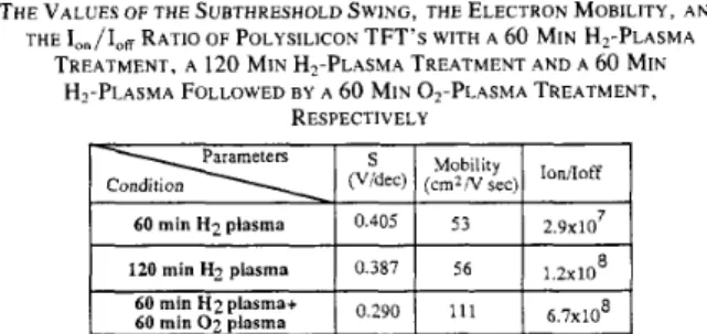
TABLE I
THE VALUES OF THE SUBTHRESHOLD SWING, THE ELECTRON MOBILITY, A N D
THE IOn,/I,,~ RATIO OF POLYSILICON TFT'S WITH A 60 MIN H?-PLASMA TREATMENT, A 120 MIN H?-PLASMA TREATMENT A N D A 60 MIN
H Z - PFOLLOWED ~ ~ ~BY A ~ 60 ~ MIN 0 2 - PTREATMENT, ~ ~ ~ ~ ~ RESPECTIVELY
on defects. The second mechanism is that it is suspected that the 02-plasma further drive in the residual hydrogen, which was originally at the gate oxide, the source end, the drain end and the bottom oxide after the H2-plasma, into the active channel region, and the 02-plasma process could crack the residually inactive hydrogen (e.g., mo- lecular hydrogen) to become active. The passivation ef- fect is thus enhanced [ 131. The improvement of H2-02- plasma treatment over the H2-plasma treatment is more apparent as the plasma-exposure time is increased. Table I complies the values of the device parameters after the devices had been subjected to a 60 min H2-plasma, a 60
min H2-plasma followed by another 60 min H,-plasma, and a 60 min H2-plasma followed by a 60 min 02-plasma. The characteristics of the 60 min H2-plasma-treated de- vice with a further 60 min H2-plasma treatment improved only slightly. The 60 min H2-plasma followed by 60 min 02-plasma-treated was the most effective in improving the device performance than a succeeding 60 min H2-plasma treatment. A further 60 min 0,-plasma caused significant improvements, especially, on the electron mobility
,
and the drain current O N / O F F ratio.It is generally recognized that the density of defect states in polysilicon is continuous across the forbidden band gap [12]. Many investigations have shown that the midgap deep-states and the exponentially distributed band tail-states affect the characteristics of polysilicon TFTs in different ways [4], [ 141, [ 151. In this work, the method of field effect conductance [8] was used to determine the density of trap states in polysilicon. The results are shown in Fig. 4 for the 60 min H2-plasma, the 60 min O,-plasma, the 20 min H2-plasma followed by 40 min 02-plasma and without plasma-treated devices. It is clearly seen that all the plasma treatment reduce the tail-state and the deep- state density significantly. The H2-plasma is more effec- tive in reducing the tail-state density and the 02-plasma is more effective in reducing the deep-state density, and the H2-02-plasma treatment is the most effective in re- ducing the tail-state density. It is also found that the ex- ponential slopes of the tail-state distribution curves be- come steeper after the plasma treatment. The extracted values of the exponential slope are 44 meV for the unpas- sivated devices, 30 meV for the H2- or the 02-plasma- treated devices and 2 3 meV for the H2-02-plasma-treated devices. These values are close to values reported in the literature [8], [ 121. The temperature dependence of the
2304 IEEE TRANSACTIONS ON ELECTRON DEVICES, VOL. 40, NO. 12, DECEMBER 1993
+Without plasma treatment
t 60 min Hiplasma
b-60 min 02-plasma
0 0.1 0.2 0.3 0.4 0.5 0.6
E
-
Ei (eV)Fig. 4 . The distributions of the trap-state densities measured by the field- effect-conductance method for the 6 0 min H,-plasma- , the 6 0 min 02- plasma- and the 20 min H,-plasma followed by 40 min 02-plasma-treated devices.
drain currents of the H,-plasma, the 0,-plasma- and the H2-02-plasma-treat devices were also measured in the temperature range from 2 0 ° C to 150°C. The activation energies of the drain currents were derived and plotted in Fig. 5 in terms of V,-Vth. The value of the activation en- ergy reflects the carrier transport barrier of the grain boundary in the polysilicon channel. A smaller trap-state density gives smaller grain-boundary potential barrier and hence, a smaller activation energy of the drain current. It is seen that the H2-plasma-treated device also has a smaller activation energy than that of the 0,-plasma-treated de- vice while the H2-02-plasma-treated device has the low- est activation energy.
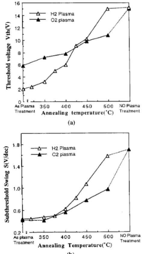
The thermal stability of the devices after they were sub- jected to different plasma-treatments was also studied. Fig. 6(a) and (b) show the threshold voltage and the subthreshold swing of the H,-plasma-treated and 02- plasma-treated devices respectively, after they were sub- jected to annealings of temperature of 320° C to 500°C in an N2 ambient. The H,-plasma-treated devices exhibited a higher degradation rate than that of the 02-plasma- treated devices. This may be due to that hydrogen has a weaker Si-H bond than the Si-0 bond and a smaller ef- fective mass than oxygen [ 161. Table I1 lists the changes of the threshold voltage, the subthreshold swing, and the Zoff of the H,-plasma (60 min)-treated device, 0,-plasma (60 min)-treated device, and the H,-plasma (20 min) fol- lowed by the 02-plasma (40 min)-treated device, after they were annealed at 4 0 0 ° C for 30 min in N2. In this table, the 02-plasma-treated device has the best thermal stabil- ity, and the H2-02-plasma-treated device and the H2- plasma-treated device have the comparable stability. The
+AV',, shift means that the V,, has increased by, for ex- ample, 1 . 3 8 V for the 60 min H2-plasma-treated device after annealing. This increase in V,, is due to the dehy-
-
No plasma treatment ... *... .... 60 min H2-plasma--
0 - - 20 min Hz-plasma + 40 min 02-plasma 0.00 " ' I " ' 0 2 4 6 8 1 0 1 2 1 4 1 6 Vg-
Vth (V)Fig. 5 . The activation energies of the drain currents for the devices of Fig. 4 plotted in terms of V,-V,,. Data were measured at Vd = 0.1 V in the temperature range from 20°C to 150°C.
16 I I
Asplasma 350 4 0 0 4 5 0 5 0 0 NOPlasma Annealing temperature('C) Treatment
(a) 0.2
1-
8 Asplasma 3 5 0 400 4 5 0 5 0 0 Noplasma Treatment Treatment Annealing Temperature("C) (b)Fig. 6. Variations of (a) the threshold voltage and (b) the subthreshold swing of the 30 min H,-plasma and the 30 min 0,-plasma-treated devices as a function of the annealing temperature. The annealing time was 30 min.
drogenation effect that the hydrogen released from the de- fect sites and caused the generation of trap states. The slight V,, decrease for 0,-plasma-treated devices after an- nealing may be due to the annealing-out of the plasma- induced damages [13]. For all the devices, thermal an- nealing decreased the Zoff. This also may be due to that the thermal treatment had annealed the plasma-induced sur- face damage [ 131. The degradation of the device perfor-
CHERN et al. : EFFECTS OF H:-O2-PLASMA TREATMENT O N THIN-FILM 1
I
.. 0.0 0.1 0.2 0 . 3 0 . 4 0.5 0 . 6 E - E i (eV) (a) I 60 min 02-plasma 0.0 0.1 0.2 0 . 3 0 . 4 0 . 5 0 . 6 E - E i (eV) (b)-
Before annealing 0 . 0 0.1 0 . 2 0 . 3 0 . 4 0 . 5 0 . 6 E-
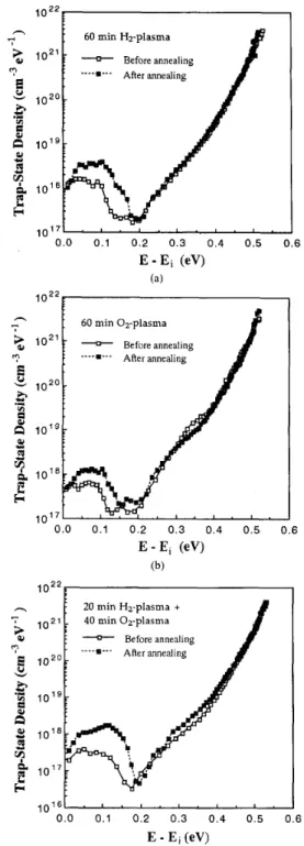
E; (eV) (C)Fig. 7 . The distributions o f the trap-state densities before and after an- nealing at 400°C for 30 min for the devices with (a) a 60 min H2-plasma treatment; (b) a 60 min 0,-plasma treatment; and (c) a 2 0 min H,-plasma followed by a 40 min 0,-plasma treatment.
mance after annealing was found to be due to the gener- ation of the deep state. Fig. 7(a)-(c) show the trap-state density distribution before and after annealing for the 60
min H2-plasma-treated, the 60 min 0,-plasma-treated and
rRANSISTORS 2305
TABLE I1
THE INCREMENT OF T H E THRESHOLD VOLTAGE, T H E SUBTHRESHOLD VOLTAGE, A N D THE LEAKAGE CURRENT AFTER ANNEALING AT 400°C
FOR 30 MIN I N A N N, AMBIENT FOR THE DEVICES W I T H A 60 MIN H*-PLASMA TREATMENT, A 60 MIN (&-PLASMA TREATMENT A N D A 20
MIN H?-PLASMA FOLLOWED BY A 4 0 MIN o,-PLASMA TREATMENT, RESPECTIVELY. THE A IS DEFINED AS THE VALUE AFTER ANNEALING-
THE VALUE BEFORE ANNEALING
0.103 0.221
the 20 min H2-plasma followed by 40 min 02-plasma- treated devices respectively. It is seen that after anneal- ing, the deep states in the energy gap between the range
of
Ei
+
0.05 eV andEi
+
0.15 eV increased for allplasma-treated devices, where
Ei
is the intrinsic Fermi- level of the polysilicon film. The tail-state density changed only slightly. Also in this figure, the 0,-plasma-treated device exhibited the least increment in the deep states. This is consistent with the result of Table 11, where the O,-plasma-treated device has the best thermal stability. It is also noted that, the deep states of the H2-02-plasma- treated device were still lower than that of the H2-plasma- treated device after the annealing.IV. CONCLUSION
In this paper, the effects of the H2-0,-plasma as well as the H2- and 0,-plasma on the electrical characteristics of polysilicon TFT’s have been studied. The H2-plasma treatment followed by 0,-plasma treatment is much more effective to passivate grain-boundary trap-states in poly- silicon films. The polysilicon TFT’s with the H2-02- plasma treatment exhibit consistently a superior perfor- mance than those with the H2-plasma treatment only or the 02-plasma treatment only. Two mechanisms are used to explain the passivation effect of the H2-02-plasma treatment. One is the passivation effect by oxygen atoms themselves and the other is the enhanced passivation ef- fect of existing hydrogen atoms to the polysilicon by the 0,-plasma. On the thermal stability, it is found that 0,-
plasma-treated devices has the best thermal stability but the H2-02-plasma-treated device exhibits a comparable thermal stability as the H,-plasma-treated device. The thermal annealing on the plasma-treated devices increase the deep states, but has no effect on the tail states of the devices.
REFERENCES
[ I ] J . Ohwada, M . Takabatake, Y . A . Ono, A . Mimura, K. Ono, and N . Konish, “Peripheral circuit integrated poly-Si TFT LCD with gray scale representation,” IEEE Trans. Eleclron Devices, vol. 36, pp.
1923-1928, Sept. 1989.
2306 IEEE TRANSACTIONS ON ELECTRON DEVICES. VOL. 40, NO. 12, DECEMBER 1993
K. Kubota, F. Matsuoka, H. Oyamatus, K. Ochii, and K. Maeguchi, “TFT (thin film transistor) cell technology for 4Mbit and more high density SRAM’s,” presented at I990 Symp. VLSI Technol., pp. 23- 24.
[3] T. Kamins and P. J. Marcoux, “Hydrogenation of transistors fabri- cated in polycrystalline silicone films,” IEEE Electron Devices Lett., vol. 1, pp. 159-161, Aug. 1980.
[4] I-W. Wu, T-Y. Huang, W. B. Jackson, A. G . Lewis, and A. C. Chiang, “Passivation kinetics of two types of defects in polysilicon TFT by plasma hydrogenation,” IEEE Electron Devices Lett., vol. 12, pp. 181-183, Apr. 1991.
[5] D . S . Ginley, “Modification of grain boundaries in polycrystalline silicon with fluorine and oxygen,” Appl. Phys. Lett., vol. 39, pp. [6] S . Ikeda, S. Hashiba, I. Kuramoto, H. Katoh, S . Ariga, T . Yaman- aka, T. Hasbimoto, N. Hashimoto and S . Meguro, “A polysilicon transistor technology for larger capacitance SRAMs,” in IEDM Tech. D i g . , 1990, pp. 459-463.
[7] H. Kitajima, Y. Suzki, and S . Saito, “Leakage current reduction in sub-micro channel poly-Si TFT’s,” in Extended Abstracts SSDM.,
[8] G . Fortunato and P. Migliorato, “Determination of gap state density in polycrystalline silicon by field-effect conductance,” Appl. Phys. Lett., vol. 49, pp. 1025-1027, 1986.
[9] U. Mitra, J. Chen, B. Khan, and E. Stupp, “Low-temperature poly- silicon TFT with gate oxide grown by high-pressure oxidation,” IEEE Electron Devices Lett., vol. 12, no. 7, pp. 390-392, 1991. [lo] W . B . Jackson, N. M . Johnson, C . C. Tasi, I.-W. Wu, A . Chiang,
and D. Smith, “Hydrogen diffusion in polycrystalline silicon thin films,” Appl. Phys. Lett., vol. 61, pp. 1670-1672, 1992. [ I l l R. Saito, Y. Sawahata and N. Momma, “A novel scaled-down oxy-
gen-implanted polysilicon resistor for future static RAM’S,” IEEE Trans. Electron Devices. vol. 35, pp. 298-301, Mar. 1988. [12] H. J . Queisser and J. H. Wemer, “Electrical and electronical prop-
erties of grain boundaries in silicon,” Mat. Res. Soc. Symp. Proc., 1131 H. N. Cbem, C. L. Lee, and T. F. Lei, “HJO, plasma on polysili- con thin film transistor,” IEEE Electron Devices Lett., vol. 14, pp. 115-1 17, Mar. 1993.
[I41 B. A. Khan and R. Pndya, “Activation energy of source-drain current in hydrogenated and unhydrogenated polysilicon thin-film transis- tor,” IEEE Trans. Electron Devices, vol. 37, pp. 1727-1734, July 1990.
[15] P. Migliorato and D. B. Meakin, “Material properties and character- istics of polysilicon transistors for large area electronics,” App. Sur- face Sci., vol. 30, p. 353, 1987.
[I61 H. N. Chem, C. L. Lee, and T . F . Lei, “Effects of H, and O2 plasma on polysilicon thin film transistor,” in Third Internat. Conf: Solid State Integrated Circuit Technol., 1992, p. 573-575.
624-627, 1981.
1991, pp. 174-176.
vol. 106, pp. 53-63, 1988.
Horng Nan Chern was bom in Tainan, Taiwan, Republic of China, on February 9 , 1967. He re- ceived the B.S. degree in electrical Engineering from National Cheng Kung University, Tainan, in 1989.
He is currently working towards the Ph.D. de- gree in the Department of Electronics engineering at National Chiao Tung University. His Ph.D. re-
search focuses on the fabrication and modeling of polysilicon thin-film transistors.
Chung Len Lee received the B . S . degree from National Taiwan University, Taiwan, R.O.C., and the M.S. and Ph.D. degrees from Camegie-Mel- lon University, Philadelphia, PA, all in electrical engineering, in 1968, 1971, and 1975, respec- tively.
He joined the Department of Electronic Engi- neering, National Chiao Tung University as a fac- ulty member in 1975 and presently he is a Profes- sor. His teaching and research have been in the areas of optoelectronics, integrated circuits and
He was the director of Semiconductor Research comuu ter-aided-design . __. _.
Cenier of the university in 1980-1983 and has been being the director of Submicron Professionals Training Center since 1989. He has supervised more than 90 M.S. and Ph.D. students in completion of their thesis. He has published more than 120 papers in joumals and conferences in the above areas.
Tan Fu Lei was bom in Keelung, Taiwan, Re- public of China, on September 17, 1944. He re- ceived the B.S. degree in the electrical engineer- ing from National Cheng Kung University, Tainan, Taiwan, in 1967 and the M.S. and Ph.D. degree in electronics engineering from National Chiao Tung University, Hsinchu, Taiwan, in 1970 and 1979, respectively.
From 1970 to 1979, he was with the Fine Prod- ucts Microelectronics Corporation, Taiwan, as an Engineer working on the fabrication of small-sig- nal transistors. From 1980 to 1982, he w& the Plant Manager of Photronic Corporation, Taiwan. In 1983, he joined the faculty at National Chiao Tung University as an Associate Professor in the Department of Electronics En- gineering and the Institute of Electronics. From 1984 to 1986, he was the Director of the Semiconductor Research Center. Presently, he is a Profes-
sor of that department and the Associate Director of National Nan0 Device Laboratory. His research interests are semiconductor devices and opto- electronics.