Enhanced Resonant Raman Scattering and Electron-Phonon Coupling from
Self-Assembled Secondary ZnO Nanoparticles
Hsin-Ming Cheng,†,‡Kuo-Feng Lin,† Hsu-Cheng Hsu,†Chih-Jen Lin,‡ Li-Jiaun Lin,‡and Wen-Feng Hsieh*,†
Department of Photonics and Institute of Electro-Optical Engineering, National Chiao Tung UniVersity, 1001 Tahsueh Road., Hsinchu 30050, Taiwan, Republic of China, and Material Research Laboratories, Industrial Technology Research Institute, Hsinchu 310, Taiwan, Republic of China
ReceiVed: June 22, 2005; In Final Form: August 9, 2005
Self-assembled secondary ZnO nanoparticles, recognized with the agglomeration of crystalline subcrystals, are successfully synthesized by a simple sol-gel method. TEM images display that one artificial cluster behaves in a single-crystal-like wurtzite structure because subcrystals coagulate as the same crystal orientation. Moreover, from the resonant Raman scattering, the as-grown sample exhibits phonon red shift; meanwhile, the coupling strength between electron and longitudinal optical phonon, determined by the ratio of second-to first-order Raman scattering cross sections, diminishes compared with the samples after postannealing at 350 and 500°C. The size dependence of electron-phonon coupling is principally as a result of the Fro¨hlich interaction.
I. Introduction
Coupling between electronic and vibrational excitations plays an important role in semiconductor materials because of its significant influence on the optoelectronic properties of semi-conductors, e.g., the transport processes, the energy relaxation rates of excited carriers, and linear or nonlinear optical absorp-tion. The electric field within materials correlates to Coulomb interaction with the exciton, and the strength of electron-phonon coupling will be enhanced if the wavelength of the phonon vibration is close to the spatial extent of the exciton.1-13
Recently, the fabrication of nanoparticles (NPs) and quantum dots (QDs) makes it possible to investigate the electron-phonon interaction beyond the bulk approximation. Such quantum-confined electronic systems differ completely from their bulk counterparts in the optical and electronic properties. Accord-ingly, a systematic study of the electron-phonon coupling strengths in semiconductor NPs and QDs is important from both the fundamental science and proposed photonic application points of view. So far, although many groups have theoretically or experimentally demonstrated the interactions between electron and phonon in III-V and II-VI semiconductor systems,1-13
contradictory results leave ambiguous answers to this basic question. As far as theory is concerned, Schmitt-Rink and co-workers1suggested that the electron-phonon coupling mediated
by the Fro¨hlich interaction should vanish with the decreasing size of GaAs and InSb QDs, by using a simple charge neutrality model. Furthermore, Alivisatos et al.2-5 presented a series of
experimental studies in CdS, CdSe, and InP nanocrystals, indicating that the electron-phonon coupling would diminish with decreasing nanocrystal size. On the contrary, Efros,6Marini
et al.,7 and Nomura and Kobayashi,8 taking into account
electron-hole correlation, valence-band degeneracy, conduction-band nonparabolicity, and properly confined phonon wave
functions, have shown that the Huang-Rhys parameter S, which measures the strength of the Fro¨hlich interaction, increases with the decreasing nanocrystal radius. Moreover, Scamarcio et al.9
reported an increase in the Fro¨hlich electron-phonon interaction strength with decreasing size in CdSxSe1-xnanocrystals
embed-ded in a glass slab. Klein et al.,10using a donorlike exciton
model but neglecting electron-hole correlation, predicted a size-independent coupling for CdSe. Experimentally, other analyses of absorption,8,11,12 photoluminescence,11,12 and spectral hole
burning13 also indicate that the electron-phonon coupling is
larger in nanocrystals with smaller radii. Because of these discrepancies, the answer to this question is still a matter of controversy.
In this article, we show the growth of high-quality ZnO NPs via a simple sol-gel method similar to that described by Seelig et al.14The secondary ZnO NPs have uniform 185 nm diameter
and are formed by the aggregation of about 9 nm primary single crystallites. The primary crystallites have an interesting self-organized behavior and then compose the texture-like poly-crystalline secondary ZnO NPs. In addition, it is also found that the enhancement of resonant Raman scattering (RRS) of the ZnO NPs, and the coupling between the lowest electronic excited state and longitudinal optical (LO) phonon modes, diminishes when compared with postannealed ZnO NPs. Zinc oxide (ZnO) is a versatile material that has achievable applica-tions in photocatalysts, varistors, sensors, piezoelectric transduc-ers, solar cells, transparent electrodes, electroluminescent de-vices, and ultraviolet laser diodes. As a result, it has stimulated extensive research.15-25 Compared to other wide band gap
materials, ZnO has a large exciton binding energy of 60 meV, which results in efficient excitonic emission at room tempera-ture. It is expected that exciton as well as polariton lasers will be fabricated, using the ZnO-related materials, and that they will overwhelm the GaN-related materials. ZnO NPs and QDs have superior optical properties of the bulk crystals owing to quantum confinement effects,26-28and more unique behaviors
are continuously being explored.
†National Chiao Tung University. ‡Industrial Technology Research Institute.
* To whom the correspondence should be addressed: Tel +886-3-5712121 ext 56316; Fax +886-3-5716631; e-mail [email protected].
10.1021/jp0533731 CCC: $30.25 © 2005 American Chemical Society Published on Web 09/10/2005
II. Experiments
The ZnO colloidal solution was produced from zinc acetate dihydrate (99.5% Zn(OAc)2, Riedel-deHaen) in diethylene
glycol (99.5% DEG, EDTA), similar to what we presented exhaustively before.29We placed the final product in a centrifuge
operating at 3000 rpm for 30 min. After this procedure, the solution was separated into two gradations. The white bottom layer included the secondary ZnO clusters, and the upper suspension was more transparent and included the dispersive single crystalline ZnO QDs. The size-dependent band gap variation of ZnO QDs was reported in our recent report.30In
this present work, we pick up the secondary ZnO clusters for investigation. The specimens were initially prepared by placing a drop of bottom solution on glass substrates and then allowed it to air-dry to remove excess solvent. Finally, the dry powders were inserted to a furnace and heated at 350 and 500°C for 1 h in air ambient.
The morphology and size distribution were characterized using a LEO-1530 field emission scanning electron microscope (FE-SEM) operated at 5 keV. The advanced microstructures of ZnO NPs were analyzed using JEOL JEM-2100F field emission transmission electron microscope (FETEM) operated at 200 keV. The phase and average crystallite size were characterized using Bede D1 thin film X-ray diffractometer (TFXRD). Conventional and resonance Raman spectroscopy were carried out by a frequency-doubled Yb:YAG laser (λ ) 515 nm) and
a He-Cd laser (λ ) 325 nm), respectively, and a Jobin-Yvon
T64000 microspectrometer with a 1800 grooves/mm grating in the backscattering configuration was employed. The whole
Raman spectra were taken with an accumulation time of 120 s from the focused incident laser light about∼1 µm. A photo-luminescence measurement was made using a 20 mW He-Cd laser at wavelength of 325 nm, and the emitted light was dispersed by a TRIAX-320 spectrometer and detected by a UV-sensitive photomultiplier tube.
III. Results and Discussion
Shown in parts a-d of Figure 1 are typical TEM micrographs of the ZnO NPs. The mean particle size is estimated to be ca. 185 nm, and the shape is essentially spherical. Hierarchical packing of the secondary ZnO NPs is formed in the condensation reactions of the sol-gel process, and the spherical shape of the ZnO NPs is recognized with agglomeration of many primary single crystallites (also called subcrystals) ranging from 6 to 12 nm. In particular, it should be noted here that when we carry out the selected area electron diffraction (SAED) for several secondary ZnO NPs, the pattern reveals the polycrystal wurtzite structure of the ZnO, as indicated in the inset of Figure 1a. On the contrary, the pattern reveals the single-crystal-like diffraction, as shown in the inset of Figure 1b, when we restrict the SAED area within only one ZnO NPs. Obviously, the secondary ZnO NPs are polycrystals consisting of much smaller subcrystals of the same crystal orientation. More evidence can be demonstrated in the high-resolution TEM (HRTEM) image and its corre-sponding fast Fourier transform image in Figure 1c. In most cases, the van der Waals interactions between the surface molecules of the nanocrystallites form the driving force for self-assembly, and then colloidal nanocrystals can be assembled to Figure 1. TEM images of secondary ZnO NPs recognized of crystalline subcrystals. (a) A typical low-magnification TEM image and SAED pattern of several uniform ZnO NPs. (b) High-magnification TEM image of one individual ZnO NP and its corresponding single-crystal-like SAED spots. (c and d) High-resolution TEM images of central area and boundary part of one individual ZnO NP, respectively.
form solids. If the size distribution of the nanocrystals is sufficiently small, ordered arrays (also called superlattices), quantum dot solids, or artificial solids are formed by self-assembly.31,32Accordingly, the growth of the secondary ZnO
NPs mentioned above must proceed in basically the same fashion, and the individual subcrystals of a particle are the subunits of a secondary ZnO NP, with some discontinuity between the subunits. Similar self-assembly structures also were reported in the R-Fe2O3 particles by Sugimoto et al.33,34The
cause of the discontinuity on the internal structure has been explained in terms of blocked fusion among the surface grains by the strong adsorption of ions used in the reaction process.35-37
However, there is no existence of other available ions during the whole process in this present work. Presumably due to the block of DEG, the solvent may behave as a microemulsion system causing the individual ZnO subcrystals that grew up separately and finally assembled to form secondary NPs under the driven force of van der Waals interaction. The subcrystals are perfect crystalline and exhibiting facets; the evidence was depicted in the HRTEM image from the edge of ZnO NPs as shown in Figure 1d. Consequently, the subcrystals self-as-sembled slowly via sintering and belong to the same definite orientation with the adjacent ones.
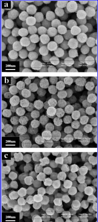
Figure 2 displays the SEM images of as-grown ZnO NPs and the samples after postannealing at 350 and 500°C in air ambient for 1 h, respectively. The evolutions of morphology in ZnO NPs show the subcrystals significantly fused with the neighbor crystals during the heating process. The grain growth also is investigated from the XRD profiles, as the crystalline sizes were estimated to be approximately 9, 14, and 20 nm for as-grown, 350 °C-annealed, and 500 °C-annealed samples, respectively, by using the Scherrer formula.
The UV Raman scattering was performed at room temperature to investigate the vibrational properties of the secondary ZnO NPs before and after being heat-treated. Since the wurtzite structure of ZnO belongs to the space group C6V4(P63mc), one
primitive cell includes two formula units, with all of the atoms occupying 2b sites of symmetry C3V. Group theory predicts the
existence of the following optic modes: A1+ 2B1+ E1+ 2E2
at theΓ point of the Brillouin zone; B1(low) and B1(high) modes
are normally silent; A1, E1, and E2modes are Raman-active;
and A1 and E1 also are infrared-active. Thus, A1 and E1 are
split into longitudinal (LO) and transverse (TO) optical com-ponents. Figure 3 shows a normal Raman spectra by a frequency-doubled Yb:YAG laser (λ ) 515 nm). As we can
see, the remarkable feature at 520 cm-1is due to the TO phonon mode from the Si substrate. The peak at 331 cm-1 can be assigned to the second-order Raman scattering arising from zone-boundary phonons 2-E2(M) of ZnO, while the peak at 437
cm-1corresponds to E2(high). Another broadened peak around
580 cm-1is contributed to the superimposition of A1(LO) and
E1(LO). We found there is no significant change of Raman
spectra for the 350°C-annealed and 500°C-annealed samples. After thermal annealing over 350°C, the intense E2(high) peak
means good crystallinity, and the full width at half-maximum (fwhm) decreases (from 14 to 11 cm-1) as the crystal size increases, which is consistent with the XRD results. Whereas, the observance of A1(LO) and E1(LO) modes are associated
with existence of some nonstoichiometric defects, such as oxygen vacancy, interstitial zinc, or their complexes38-40in the
secondary ZnO NPs after heating treatment.
In previous resonant Raman scattering (RRS) experiments, in principle the electron phonon interaction could be straightly probed. A He-Cd laser (λ ) 325 nm) was used as the excitation
source for RRS. The exciting photon energy is resonant with the electronic interband transition energy of the wurtzite ZnO. The polar symmetry makes the A1(LO) and E1(LO) modes the
dominant modes, and it may exhibit different frequencies from the TO modes. An intense multiphonon scattering of the secondary ZnO NPs before and after heat treatment was observed in the resonant Raman spectrum of Figure 4, where four major bands were observed to mainly result from the polar symmetry modes A1(LO) and E1(LO) and their overtones. The
first-order Raman mode is a superposition of the LO phonon mode in which Zn atoms and O atoms have the same vibration direction, respectively, to the neighbor lattices of the wurtzite ZnO.41The weak peak, which is contributed to the E
2(high)
mode around 437 cm-1, is almost imperceptible as a result of other stronger RRS peaks. Multiphonon scattering processes also have been previously reported for single crystalline bulk ZnO42
Figure 2. SEM micrographs of (a) as-grown, (b) 350°C annealing for 1 h, and (c) 500°C annealing for 1 h secondary ZnO NPs.
and recently for ZnO films,43ZnO opal structures,44and ZnO
nanowires45,46but rarely mentioned for ZnO NPs. From the RRS
spectra, it is remarkable that the intensities of the first-order Raman mode and its overtones are enhanced in the as-grown ZnO NPs compared with the postannealed samples. The reason can be explained using the total Raman cross section for an
n-phonon process written as2,10
whereµ is the electronic dipole transition moment, E0is the
size-dependent energy of the electronic transition, pω and pωLO
are the energies of the incident photon and the LO phonon, respectively, m denotes the intermediate vibrational level in the excited state,Γ is the homogeneous line width, kB is
Boltz-mann’s constant, T is the temperature, and the bracket indicates
the overlap integral between the ground and excited states wave functions. Consequently, RRS intensity can be enhanced as a result of the energy of the incoming or the scattered photons, to match real electronic states in the material and cause the denominator in the Raman scattering cross section to tend to zero. Similar results have been previously reported for CdS and ZnO, using various laser wavelengths.47In our case, the band
gap of as-grown ZnO NPs would tend to approach the excitation laser energy because of the quantum-confined effect as the subcrystal size is relative to the exciton radius.30The
quantum-confined evidence can be seen as the intensive tail of the blue-shift photoluminescence (PL) signal of the as-grown sample and also discovered in RRS spectra rather than normal RS spectra, as a result of the red shift, broadening, and the asymmetry of the first-order optical phonon mode of the smaller ZnO NPs. It is well-known that phonon eigenstates in an ideal crystal are plane waves due to the infinite correlation length; therefore, the K ) 0 momentum selection rule of the first-order Raman spectrum can be satisfied. When the crystalline is reduced to nanometer scale, the momentum selection rule will be relaxed. This allows the phonon with wave vector|k| ) |k′| ( 2π/L to participate in the first-order Raman scattering, where k′is the wave vector of the incident light and L is the size of the crystal. The phonon scattering will not be limited to the center of the Brillouin zone, and the phonon dispersion near the zone center must also be considered so that the shift, broadening, and the asymmetry of the first-order optical phonon can be observed. In recently reported studies, Alim et al.48,49 have shown that
the large red shifts in the resonant Raman spectra from 20 nm ZnO NPs are most likely due to the local heating by UV laser excitation. In our study, since the as-grown secondary ZnO NPs contain more air gaps than the annealed ones, the smaller thermal conductivity may become one of the other possibilities which results in higher temperatures and larger phonon red shift. The detailed numerical analysis of ZnO NPs of this experiment is distinctively listed at Table 1 for clarity.
Furthermore, the ratio between second- and first-order Raman scattering cross sections was found to increase remarkably from 0.38 to 2.05 with an increase of the ZnO crystallite size from nanoparticle to the bulk. Within the Franck-Condon ap-proximation,50,51the coupling strength of the exciton transitions
to the LO phonon may be expressed in terms of Huang-Rhys parameter S. The cross section of RRS was a function of particle size, temperature, and excitation wavelength. Scamarico et al.9
suggested that keeping constant the resonance condition is mandatory for a meaningful comparison of spectra associated with nanocrystals having different sizes and hence different electron transitions, due to the strong energy dependence of the Raman scattering cross section. In this study, we have carefully used the same experimental conditions, such as laser wavelength, power, spot size, and so on for each sample. We reported here Figure 3. Normal Raman spectra of (a) as-grown, (b) 350°C annealing
for 1 h, and (c) 500°C annealing for 1 h secondary ZnO NPs, using a frequency-doubled Yb:YAG laser (λ ) 515 nm).
Figure 4. Resonant Raman scatterings (RRS) of (a) as-grown, (b) 350 °C annealing for 1 h, and (c) 500°C annealing for 1 h secondary ZnO NPs, using a He-Cd laser (λ ) 325 nm).
σn)
∫
σnR(ω) f (R) dR (1) σn R (ω) ) µ4|∑
m)0 ∞ 〈n|m〉〈m|0〉 E0+ npωLO-pω + ipΓ |2 exp(
-ipωLO kBT)
(2)TABLE 1: Wavenumber, Broadening, and the Ratio of
n-LO Phonons Found in RRS Spectra; the Assignments of
Bulk ZnO Are Also Listed as a Reference
as-growna 350°Ca 500°Ca bulkb grain size (nm) 9 14 20 >1000 1LO (cm-1) 578 582 584 585 (fwhm) (27.2) (24.2) (23.9) (N/A) 2LO (cm-1) 1149 1154 1158 1165 (fwhm) (54.7) (49.3) (47.3) (N/A) I2LO/I1LO 0.38 0.59 1.07 2.05
aThis work.bFrom ref 42 (used the same He-Cd laser,λ ) 325
with an emphasis on the tendency of the increasing electron-phonon interaction with increasing nanocrystal size. It is generally accepted that the electron-phonon coupling is deter-mined by two mechanisms: the deformation potential and the Fro¨hlich potential. Following Loudon52and Kaminow,53the TO
Raman scattering cross section is mainly determined by the deformation potential that involves the short-range interaction between the lattice displacement and the electrons. On the other hand, the LO Raman scattering cross section includes contribu-tions from both the Fro¨hlich potential that involves the long-range interaction generated by the macroscopic electric field associated with the LO phonons and the deformation potential. We found that the intensity of TO phonon in ZnO NPs is almost insensitive, while that of LO phonon is greatly enhanced under the resonant conditions. Therefore, we believe that the electron-LO phonon coupling as decreasing the nanocrystal size is mainly associated with the Fro¨hlich interaction. Although the complex origin is not well understood, the result in this study is extremely consistent with recently reports in other low-dimensional ZnO nanosystems, such as the ZnO nanowires54 and ZnO-based
quantum wells.55
Figure 5 shows the normalized room temperature PL spectra of the as-grown and the heat-treated ZnO NPs. As we can see, the UV emission peaks, which were attributed to the exciton-related recombination, slightly shift their position from 376 to 387 nm after heat treatment. The band gap enlargement happens to the as-grown ZnO sample that results in enhancing the intensity of RRS, as mentioned above. Then, the grain grows after the annealing process, resulting in the optical property returning back to the bulk similarity. Besides, some various impurity exciton complexes also probably cause the shifts of UV emission from ZnO NPs. Fonoberov et al.56,57 have
theoretically reported two possible sources of UV PL in ZnO QDs, which have been considered as excitons confined in the quantum dot and excitons bound to an ionized impurity located at the quantum-dot surface. Compared with the bulk ZnO, the slightly blue shift of UV photoluminescence in our as-grown ZnO NPs was due to the influence of size effect on energy level of confined excitons. Moreover, the UV photoluminescence peaks of postannealed ZnO samples red-shifted from the general bulk free exciton energy (∼3.31 eV at 298 K) as far as more than 100 meV. Therefore, we argue that the red shifts may be caused by the presence of acceptors bound excitons if there are existing numerous impurities at the surface of ZnO NPs after annealing at the high temperature. So far, the opinions are in agreement with ref 56, and the more accurate possibility of UV transition indeed needs to be further confirmed. In addition, a broadening visible band, from 500 to 700 nm, appears gradually when raising the heating temperature. It is generally agreed that
the visible emission is due to nonstoichiometric composition, and visible PL is most commonly green, though other peaks such as, for example, yellow and orange emissions also can be observed which come from oxygen vacancies (VO),58oxygen
interstitials (Oi),59and ionic dopants.60In our room temperature
PL spectra, the broad yellow emission at local maximum position 600 nm was observed; such a deep level involved in the yellow luminescence of ZnO is attributed to oxygen interstitials (Oi). The origin is due to oxygen diffusion of the
ZnO NPs after annealing in the atmosphere and also is consistent with the previous study for ZnO samples sintered in moist air.61
Furthermore, Greene et al.62have provided strong evidence of
the disappearance of the yellow emission in oxygen-deficient ZnO nanowires after reducing treatment. Consequently, the yellow emission in our present work is associated with oxygen interstitials, beyond all doubt.
IV. Conclusion
In summary, we have demonstrated the self-assembled secondary ZnO nanoparticles recognized with the agglomeration of crystalline subcrystals ranging from 6 to 12 nm synthesized by a sol-gel method. From TEM analyses, the artificial clusters behave like a single-crystal structure, owing to the subcrystals coagulating as the same crystal orientation with adjacent ones via the sintering process. The as-grown sample exhibits phonon red shift in a resonant Raman scattering, compared with the samples after postannealing at 350 and 500°C. Moreover, the electron-phonon coupling parameter is unambiguously ex-tracted from resonant Raman scattering, and an interesting phenomenon of increasing electron-LO phonon coupling is also be discovered when the crystal size of ZnO enlarges after heating treatment. The tendency of the size-dependent electron-phonon coupling in the 0-D ZnO particles is similar to other 1-D and 2-D ZnO systems. The Fro¨hlich interaction certainly plays the main role in the coupling of ZnO particles. Finally, the blue shift of UV photoluminescence and visible emission induced by oxygen interstitial (Oi) were also to be investigated from
the as-grown and the heated ZnO samples, respectively.
Acknowledgment. The authors gratefully acknowledge financial support from the National Science Council (NSC) of Taiwan under Contract NSC-93-2112-M-009-035. We also thank the Nano Technology Research Center (NTRC/ITRI) for facilities support and the TEM group of MRL/ITRI for great help on electron microscopy measurements.
References and Notes
(1) Rink, S.; Miller, D. A. B.; Chemla, D. S. Phys. ReV. B 1987, 35, 8113.
(2) Alivisatos, A. P.; Harris, T. D.; Carroll, P. J.; Steigerwald, M. L.; Brus, L. E. J. Chem. Phys. 1989, 90, 3463.
(3) Shiang, J. J.; Goldstein, A. N.; Alivisatos, A. P. J. Chem. Phys.
1990, 92, 3232.
(4) Shiang, J. J.; Risbud, S. H.; Alivisatos, A. P. J. Chem. Phys. 1993,
98, 8432.
(5) Shiang, J. J.; Wolters, R. H.; Heath, J. R. J. Chem. Phys. 1997,
106, 8981.
(6) Efros, A. L. Solid State Commun. 1991, 78, 853.
(7) Marini, J. C.; Stebe, B.; Kartheuser, E. Phys. ReV. B 1994, 50, 14302.
(8) Nomura, S.; Kobayashi, T. Phys. ReV. B 1992, 45, 1305. (9) Scamarcio, G.; Spagnolo, V.; Ventruti, G.; Lugara, M.; Righini, G. C. Phys. ReV. B 1996, 53, R10489.
(10) Klein, M. C.; Hache, F.; Ricard, D.; Flyzanis, C. Phys. ReV. B 1990,
42, 11123.
(11) Banyai, L.; Hu, Y. Z.; Lindberg, M.; Koch, S. W. Phys. ReV. B
1988, 38, 8142.
(12) Itho, T.; Nishijima, M.; Ekimov, A. I.; Gourdon, C.; Efros, A. L.; Rosen, M. Phys. ReV. Lett. 1995, 74, 1645.
Figure 5. Normalized room temperature PL spectra of the secondary ZnO NPs before and after heat treatment.
(13) Roussignol, P.; Ricard, D.; Flytzanis, C.; Neuroth, N. Phys. ReV.
Lett. 1989, 62, 312.
(14) Seelig, E. W.; Tang, B.; Yamilov, A.; Cao, H.; Chang, R. P. H.
Mater. Chem. Phys. 2003, 80, 257.
(15) Lin, F. C.; Takao, Y.; Shimizu, Y.; Egashira, M. Sens. Actuators
B 1995, 24, 843.
(16) Weissenrieder, K. S.; Muller, J. Thin Solid Films 1997, 30, 300. (17) Minne, S. C.; Manalis, S. R.; Quate, C. F. Appl. Phys. Lett. 1995,
67, 3918.
(18) Baxter, J. B.; Aydil, E. S. Appl. Phys. Lett. 2005, 86, 053114. (19) Law, M.; Greene, L.; E. Johnson, J. C.; Saykally, R.; Yang, P.
Nat. Mater. 2003, 2, 673.
(20) Hoffman, R. L.; Norris, B. J.; Wager, J. F. Appl. Phys. Lett. 2003,
82, 733.
(21) Tang, Z. K.; Wong, G. K. L.; Yu, P.; Kawasaki, M.; Ohtomo, A.; Koinuma, H.; Segawa, Y. Appl. Phys. Lett. 1998, 72, 3270.
(22) Fan, Z.; Wang, D.; Chang, P. C.; Tseng, W. Y.; Lu, J. G. Appl.
Phys. Lett. 2004, 85, 5923.
(23) Park, W. I.; Yi, G. C. AdV. Mater. 2004, 16, 87.
(24) Yi, G. C.; Wang, C.; Park, W. I. Semicond. Sci. Technol. 2005,
20, S22.
(25) Heo, Y. W.; Norton, D. P.; Tien, L. C.; Kwon, Y.; Kang, B. S.; Ren, F.; Pearton, S. J.; LaRoche, J. R. Mater. Sci. Eng., R 2004, 47, 1.
(26) Germeau, A.; Roest, A. L.; Vanmaekelbergh, D.; Allan, G.; Delerue, C.; Meulenkamp, E. A. Phys. ReV. Lett. 2003, 90, 097401.
(27) Cao, H.; Zhao, Y.; Ho, S. T.; Seelig, E. W.; Wang, Q. H.; Chang, R. P. H. Phys. ReV. Lett. 1999, 82, 2278.
(28) Wu, X.; Yamilov, A.; Noh, H.; Cao, H.; Seelig, E. W.; Chang, R. P. H. J. Opt. Soc. Am. B 2004, 21, 159.
(29) Cheng, H. M.; Hsu, H. C.; Chen, S. L.; Wu, W. T.; Kao, C. C.; Lin, L. J.; Hsieh, W. F. J. Cryst. Growth 2005, 277, 192.
(30) Lin, K. F.; Cheng, H. M.; Hsu, H. C.; Lin, L. J.; Hsieh, W. F.
Chem. Phys. Lett. 2005, 409, 208.
(31) Murray, C. B.; Kagan, C. R.; Bawendi, M. G. Science 1995, 270, 1335.
(32) Murray, C. B.; Sun, S. H.; Gaschler, W.; Doyle, H.; Betley, T. A.; Kagan, C. R. IBM J. Res. DeV. 2001, 45, 47.
(33) Park, G.; Shindo, D.; Waseda, Y.; Sugimoto, T. J. Colloid Interface
Sci. 1996, 177, 198.
(34) Sugimoto, T.; Wang, Y.; Itoh, H.; Muramatsu, A. Colloids Surf.,
A 1998, 134, 265.
(35) Sugimoto, T.; Sakata, K.; Muramatsu, A. J. Colloid Interface Sci.
1993, 159, 372.
(36) Sugimoto, T.; Khan, M. M.; Muramatsu, A. Colloids Surf., A 1993,
79, 233.
(37) Sugimoto, T.; Muramatsu, A.; Sakata, K.; Shindo, D. J. Colloid
Interface Sci. 1993, 158, 420.
(38) Exarhos, G. J.; Sharma, S. K. Thin Solid Films 1995, 270, 27. (39) Xu, X. L.; Lau, S. P.; Chen, J. S.; Che, G. Y.; Tay, B. K. J. Cryst.
Growth 2001, 223, 201.
(40) Ashkenov, N.; Mbenkum, B. N.; Bundesmann, C.; Riede, V.; Lorenz, M.; Spemann, D.; Kaidashev, E. M.; Kasic, A.; Schubert, M.; Grundmann, M.; Wagner, G.; Neumann, H.; Darakchieva, V.; Arwin, H.; Monemar, B. J. Appl. Phys. 2003, 93, 126.
(41) Damen, T. C.; Porto, S. P. S.; Tell, B. Phys. ReV. 1966, 142, 570. (42) Scott, J. F. Phys. ReV. B 1970, 2, 1209.
(43) Zhang, X. T.; Liu, Y. C.; Zhi, Z. Z.; Zhang, J. Y.; Lu, Y. M.; Shen, D. Z.; Xu, W.; Zhong, G. Z.; Fan, X. W.; Kong, X. G. J. Phys. D 2001, 34, 3430.
(44) Ursaki, V. V.; Tiginyanu, I. M.; Zalamai, V. V.; Masalov, V. M.; Samarov, E. N.; Emelchenko, G. A.; Briones, F. J. Appl. Phys. 2004, 96, 1001.
(45) Ng, H. T.; Chen, B.; Li, J.; Han, J.; Meyyappan, M.; Wu, J.; Li, S. X.; Haller, E. E. Appl. Phys. Lett. 2003, 82, 2023.
(46) Cheng, H. M.; Hsu, H. C.; Tseng, Y. K.; Lin, L. J.; Hsieh, W. F.
J. Phys. Chem. B 2005, 109, 8749.
(47) Callender, R. H.; Sussman, S. S.; Selders, M.; Chang, R. K. Phys.
ReV. B 1973, 7, 3788.
(48) Alim, K. A.; Fonoberov, V. A.; Balandin, A. A. Appl. Phys. Lett.
2005, 86, 053103.
(49) Alim, K. A.; Fonoberov, V. A.; Shamsa, M.; Balandin, A. A. J.
Appl. Phys. 2005, 97, 124313.
(50) Bartolo, B. D.; Powell, R. Phonons and Resonances in Solids; Wiley: New York, 1976; Chapter 10.
(51) Bo¨er, K. W. SurVey of Semiconductor Physics; Van Nostrand Reinhold: New York, 1990; Chapter 20.
(52) Loudon, R. AdV. Phys. 1964, 13, 23.
(53) Kaminow, I. P.; Johnston, W. D. Phys. ReV. 1967, 160, 19. (54) Wang, R. P.; Xu, G.; Jin, P. Phys. ReV. B 2004, 69, 113303. (55) Makino, T.; Tamura, K.; Chia, C. H.; Segawa, Y.; Kawasaki, M.; Ohtomo, A.; Koinuma, H. Phys. ReV. B 2002, 66, 233305.
(56) Fonoberov, V. A.; Balandin, A. A. Appl. Phys. Lett. 2004, 85, 5971. (57) Fonoberov, V. A.; Balandin, A. A. J. Phys.: Condens. Matter 2005,
17, 1085.
(58) Vanheusden, K.; Warren, W. L.; Seager, C. H.; Tallant, D. R.; Voigt, J. A.; Gnade, B. E. J. Appl. Phys. 1996, 79, 7983.
(59) Wu, X. L.; Siu, G. G.; Fu, C. L.; Ong, H. C. Appl. Phys. Lett.
2001, 78, 2285.
(60) Studenikin, S. A.; Golego, N.; Cocivera, M. J. Appl. Phys. 1998,
84, 2287.
(61) Liu, M.; Kitai, A. H.; Mascher, P. J. Lumin. 1992, 54, 35. (62) Greene, L. E.; Law, M.; Goldberger, J.; Kim, F.; Johnson, J. C.; Zhang, Y.; Saykally, R. J.; Yang, P. Angew. Chem., Int. Ed. 2003, 42, 3031.