258 IEEE ELECTRON DEVICE LETTERS, VOL. 27, NO. 4, APRIL 2006
High-Performance Poly-Si TFTs With
Fully Ni-Self-Aligned Silicided
S/D and Gate Structure
Po-Yi Kuo, Tien-Sheng Chao, Senior Member, IEEE, Ren-Jie Wang, and Tan-Fu Lei, Member, IEEE
Abstract—In this letter, fully Ni self-aligned silicided (fully
Ni-salicided) source/drain (S/D) and gate polycrystalline silicon thin-film transistors (FSA-TFTs) have been successfully fabricated on a 40-nm-thick channel layer. Experimental results show that the FSA-TFTs give increased ON/OFF current ratio, improved subthreshold characteristics, less threshold voltage rolloff, and larger field-effect mobility compared with conventional TFTs. The FSA-TFTs exhibit small S/D and gate parasitic resistance and effectively suppress the floating-body effect and parasitic bipolar junction transistor action. The characteristics of the FSA-TFTs are suitable for high-performance driving TFTs with good output characteristics and large breakdown voltage.
Index Terms—Floating-body effect, fully salicided, parasitic
bipolar junction transistor, polycrystalline silicon thin-film tran-sistors (poly-Si TFTs).
I. INTRODUCTION
R
ECENTLY, polycrystalline silicon thin-film transistors (poly-Si TFTs) have been widely used in many applica-tions, particularly as the integrated peripheral driving circuits and addressing elements in active-matrix liquid-crystal displays (AMLCDs) [1], [2]. However, the output characteristics exhibit an anomalous increase of current in the saturation regime, often called the “kink” effect because of an analogy with silicon-on-insulator (SOI) devices [3]–[5]. This phenomenon can be attributed to the floating-body effect [6] and the avalanche multiplication enhanced by grain boundary traps [4]. With increasing drain voltage, the added drain current enhances impact ionization and parasitic bipolar junction transistor (BJT) effect, which leads to a premature breakdown in return [6]. In the floating-body thin-film devices, the improved parasitic BJT effect can be achieved by using deep salicidation and fully silicided source/drain (S/D) structure [7], [8]. Similar to SOI devices, the thin-channel poly-Si TFTs exhibit improved device characteristics such as small leakage current and suppressed floating-body effect compared with the thick-channel poly-SiManuscript received November 4, 2005; revised January 6, 2006. This work was supported by the National Science Council (NSC), Taiwan, R.O.C., under Contract NSC-94-2215-E-009-064. The review of this letter was arranged by Editor J. Sin.
P.-Y. Kuo and T.-F. Lei are with the Department of Electronics Engineering and Institute of Electronics, National Chiao-Tung University, Hsinchu 30010, Taiwan, R.O.C.
T.-S. Chao and R.-J. Wang are with the Department of Electrophysics, National Chiao-Tung University, Hsinchu 30010, Taiwan, R.O.C.
Digital Object Identifier 10.1109/LED.2006.870417
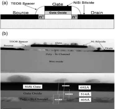
Fig. 1. (a) Schematic device structure and (b) TEM micrograph of the FSA-TFTs with gate length of 0.8 µm and channel thickness of 40 nm.
TFTs [9]. However, parasitic S/D resistances have increasingly become a serious issue in the thin-channel poly-Si TFTs. Several methods such as self-aligned silicide and selective tungsten-clad technology were proposed to reduce parasitic S/D resistance for thin-channel SOI MOSFETs and poly-Si TFTs [8], [10], [11]. In addition, silicided gates have a higher capacitance than poly-Si gates due to the elimination of poly-Si depletion [12].
In this letter, fully Ni self-aligned silicided (fully Ni-salicided) S/D and gate poly-Si thin-film transistors (FSA-TFTs), whose S/D and gate layers are completely silicided with Ni, have been successfully fabricated on a 40-nm-thick channel layer. We found that the measured characteristics of the FSA-TFTs with in situ n+-doped gate or undoped gate signifi-cantly suppressed floating-body and parasitic BJT effects.
II. EXPERIMENT
The schematic device structure and transmission electron microscopy (TEM) micrograph of the FSA-TFTs is shown in Fig. 1. The FSA-TFTs were fabricated using the following
KUO et al.: POLY-Si TFTs WITH Ni SELF-ALIGNED SILICIDED S/D AND GATE STRUCTURE 259
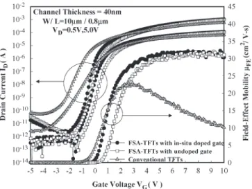
Fig. 2. Measured transfer characteristics and field-effect mobility of the conventional TFTs and the FSA-TFTs with W/L = 10 µm/0.8 µm.
process steps. First, a 40-nm amorphous-silicon (a-Si) layer was deposited by low-pressure chemical vapor deposition (LPCVD) at 550◦C on oxidized silicon wafers. Next, the a-Si layer was crystallized by solid-phase crystallization (SPC) at 600◦C for 24 h. After the active-region patterning, a 50-nm tetraethoxysi-lane (TEOS) gate oxide layer was deposited by LPCVD. Sub-sequently, a 50-nm a-Si gate layer and a 150-nm Si3N4layer as
the hard mask were deposited by LPCVD. The a-Si gate layers were divided into in situ n+ phosphorus-doped gate or
un-doped gate. After identifying the gate electrode, a self-aligned implantation was used to form the n+ S/D with p+ to dose
5× 1015cm−2. Dopants were activated by a furnace at 600◦C
for 12 h. A 150-nm TEOS oxide was deposited and etched to form the sidewall spacer. Then, the Si3N4 hard-mask layer
was selectively etched in a hot phosphoric-acid bath. A Ni film of about 40 nm was deposited by sputtering, and then full Ni salicidation was carried out at 550◦C for 60 s by a one-step rapid thermal annealing (RTA) in the N2ambient. The fully
Ni-silicided S/D and gate were formed by the full Ni salicidation. After contact and metallization processes, hydrogenation pro-cedures were implemented after sintering at 400◦C for 30 min. Conventional devices with self-aligned n+S/D and without Ni
salicidation were also fabricated to serve as controls. III. RESULTS ANDDISCUSSION
The measured transfer characteristics and field-effect mobil-ity of the conventional TFTs and the FSA-TFTs with W/L = 10 µm/0.8 µm are shown in Fig. 2. The ON-state currents and field-effect mobility in the FSA-TFTs are higher than in the conventional TFTs. TheON-state currents are significantly degraded by the parasitic S/D resistance in short-channel con-ventional TFTs. The field-effect mobility plotted in Fig. 2 is obtained from the channel conductance. For the conventional TFTs with a short-channel length of 0.8 µm, the field-effect mobility is seriously decreased when gate voltage VG> 2.5 V,
but it is not found in short-channel FSA-TFTs. This improve-ment is due to the fully Ni-salicided S/D and gate structure,
Fig. 3. Extracted threshold voltage VTHof the conventional TFTs and the
FSA-TFTs with different gate lengths (defined as ID= W/L× 100 nA at
VDS= 0.5 V).
which has smaller parasitic S/D resistance, higher capaci-tance, and superior scalability than the conventional TFTs with poly-Si gates [12]. Furthermore, an anomalous subthreshold swing (SS) and an unstable VTH are observed in conventional
TFTs with W/L = 10 µm/0.8 µm at VDS= 5.0 V. Fig. 3
dis-plays the extracted threshold voltage VTH of the conventional
TFTs and the FSA-TFTs with different gate lengths (defined as ID= W/L× 100 nA at VDS= 0.5 V). The rolloff of the
threshold voltage VTHis greatly improved in FSA-TFTs. With
this fully Ni-salicided structure in FSA-TFTs, the floating-body and parasitic bipolar effects can be suppressed, resulting in a stable VTHand a lowerOFF-state leakage current [7], [8], [13],
[14]. Therefore, the ON/OFF current ratio (108−109) can be
increased by scaling down the channel length in FSA-TFTs. The advantage of FSA-TFTs can be found also on SS. We believe that it may be due to the higher gate capacitance and the fully silicided S/D in the FSA-TFTs.
Fig. 3 also shows the VTH difference (0.5–0.6 V) between
in situ n+-doped gate and undoped gate FSA-TFTs. This VTH
shift is observed with additional p+ dopants in the in situ n+
-doped gate FSA-TFTs. The silicidation-induced segregation of the impurities from poly-Si to the silicide interface indicated that submonolayer segregation of the dopants causes a change in the apparent Ni/Si work-function shift [12].
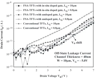
Fig. 4 exhibits the measuredOFF-state leakage currents of the conventional TFTs and the FSA-TFTs with different channel lengths at VG=−5.0 V. The enhancement ofOFF-state
leak-age currents is observed in short-channel conventional TFTs. These enhanced OFF-state leakage currents are the amplifi-cation of gate-induced-drain leakage (GIDL) currents by the parasitic BJT in short-channel devices due to the floating-body effect [15]. Inasmuch as the FSA-TFTs effectively suppress the floating-body effect, the enhancement of GIDL currents is eliminated, and OFF-state leakage currents are almost the same in both long- and short-channel devices. Due to the work-function difference of Ni/Si gates between in situ n+-doped
260 IEEE ELECTRON DEVICE LETTERS, VOL. 27, NO. 4, APRIL 2006
Fig. 4. MeasuredOFF-state leakage currents of the conventional TFTs and the FSA-TFTs with W/L = 10 µm/10 µm and W/L = 10 µm/0.8 µm at VG=−5.0 V.
Fig. 5. Measured output characteristics of the conventional TFTs and the FSA-TFTs with W/L = 10 µm/0.8 µm.
gate and undoped gate FSA-TFTs, a drain-voltage shift ofOFF -state leakage currents is observed [16].
The measured output characteristics of the conventional TFTs and the FSA-TFTs with W/L = 10 µm/0.8 µm are shown in Fig. 5. Under high drain voltage, the accumulation of holes in the body causes a profound kink effect and an induced parasitic BJT action, which results in decreased drain breakdown voltage by the floating-body effect in the conven-tional TFTs [17]–[20]. Salicidation is a well-known method to suppress the floating-body effect, because the silicide layer near the S/D junction works as a sink and an effective lifetime killer for holes [7], [8]. The reduced kink effect and the increased drain breakdown voltage of FSA-TFTs strongly support the idea that floating-body and parasitic BJT effects are signifi-cantly suppressed by the fully silicided S/D structure.
IV. CONCLUSION
We have developed the fully Ni-salicided S/D and gate poly-Si TFTs to suppress the floating-body effect. The enhancement of GIDL currents that occurred in the conventional TFTs is eliminated by the FSA-TFTs. The FSA-TFTs show reduced kink effect, increased breakdown voltage, stable VTH, improved
SS, and increased ON/OFF current ratio. The FSA-TFTs are proven to be a very promising structure with low S/D parasitic resistance and high gate capacitance capability fabricated on a thin 40-nm-thick channel layer.
ACKNOWLEDGMENT
The authors would like to thank the Nano Facility Center (NFC) of the National Chiao-Tung University and the Na-tional Nano Device Laboratory (NDL) for providing process equipment.
REFERENCES
[1] A. G. Lewis, I.-W. Wu, T. Y. Huang, A. Chiang, and R. H. Bruce, “Active matrix liquid crystal display design using low and high temper-ature processed polysilicon TFTs,” in IEDM Tech. Dig., San Francisco, CA, 1990, pp. 843–846.
[2] H. Oshima and S. Morozumi, “Feature trends for TFT integrated circuits on glass substrates,” in IEDM Tech. Dig., Washington, DC, p. 157, 1989.
[3] M. Koyanagi, H. Kurino, T. Hashimoto, H. Mori, K. Hata, Y. Hiruma, T. Fujimori, I.-W. Wu, and A. G. Lewis, “Relation between hot-carrier light emission and kink-effect in poly-Si thin film transistors,” in IEDM
Tech. Dig., Washington, DC, 1991, p. 571.
[4] M. Hack and A. G. Lewis, “Avalanche-induced effects in polysilicon thin-film transistors,” IEEE Electron Device Lett., vol. 12, no. 5, pp. 203–205, May 1990.
[5] J. P. Colinge, “Reduction of kink effect in thin-film SOI MOSFETs,”
IEEE Electron Device Lett., vol. 9, no. 2, pp. 97–99, May 1988.
[6] M. Valdinoci, L. Colalongo, G. Baccarani, G. Fortunato, A. Pecora, and I. Policicchio, “Floating body effects in polysilicon thin-film transis-tors,” IEEE Trans. Electron Devices, vol. 44, no. 12, pp. 2234–2241, Dec. 1997.
[7] F. Deng, R. A. Johnson, W. B. Dubbeldav, G. A. Garcia, P. M. Asbeck, and S. S. Lau, “Deep salicidation using nickel for suppressing the floating body effect in partially depleted SOI-MOSFET,” in Proc. IEEE Int. SOI
Conf., Sanibal Island, FL, 1996, pp. 78–79.
[8] T. Ichimori and N. Hirashita, “Fully-depleted SOI CMOSFETs with the fully-silicided source/drain structure,” IEEE Trans. Electron Devices, vol. 49, no. 12, pp. 2296–2300, Dec. 2002.
[9] M. Miyasaka, T. Komatsu, W. Itoh, A. Yamaguchi, and H. Ohshima, “Effects of semiconductor thickness on poly-crystalline silicon thin film transistors,” Jpn. J. Appl. Phys., vol. 35, no. 2B, pp. 923–929, Feb. 1996. [10] H. W. Zen, T. C. Chang, P. S. Shih, D. Z. Peng, P. Y. Kuo, T. Y. Huang,
C. Y. Chang, and P. T. Lin, “A study of parasitic resistance effects in thin-film polycrystalline silicon TFTs with Tungsten-clad S/D,” IEEE Electron
Device Lett., vol. 24, no. 8, pp. 509–512, Aug. 2003.
[11] K. H. Lee, J. K. Park, and J. Jang, “A high-performance polycrystalline silicon thin film transistor with a silicon nitride gate insulator,” IEEE
Trans. Electron Devices, vol. 45, no. 12, pp. 2548–2551, Dec. 1998.
[12] J. Kedzierski, D. Boyd, C. Cabral, Jr., P. Ronsheim, S. Zafar, P. M. Kozlowski, J. A. Ott, and M. Ieong, “Threshold voltage control in NiSi-gated MOSFETs through SIIS,” IEEE Trans. Electron Devices, vol. 52, no. 1, pp. 39–46, Jan. 2005.
[13] M. Chan, B. Yu, Z. J. Ma, C. T. Nguyen, C. Hu, and P. K. Ko, “Compar-ative study of fully depleted and body-grounded non fully depleted SOI MOSFETs for high performance analog and mixed signal circuits,” IEEE
Trans. Electron Devices, vol. 42, no. 11, pp. 1975–1981, Nov. 1995.
[14] H. F. Wei, J. E. Chung, N. M. Kalkhoran, and F. Namavar, “Suppres-sion of parasitic bipolar effects and off-state leakage in fully-depleted SOI n-MOSFET’s using Ge-implantation,” IEEE Trans. Electron Devices, vol. 42, no. 12, pp. 2096–2103, Dec. 1995.
[15] J. Chen, F. Assaderaghi, P. K. Ko, and C. Hu, “The enhancement of gate-induced-drain-leakage (GIDL) current in short-channel SOI MOSFET
KUO et al.: POLY-Si TFTs WITH Ni SELF-ALIGNED SILICIDED S/D AND GATE STRUCTURE 261
and its application in measuring lateral bipolar current gain β,” IEEE
Electron Device Lett., vol. 13, no. 11, pp. 572–574, Nov. 1992.
[16] ——, “The enhancement of gate-induced-drain-leakage (GIDL) current in SOI MOSFET and its impact on SOI device scaling,” in Proc. IEEE
Int. SOI Conf., Ponte Vedra Beach, FL, 1992, pp. 84–85.
[17] S. Yamada, S. Yokoyama, and M. Koyanagi, “Two-dimensional device simulation for avalanche induced short channel effect in poly-Si TFT,” in
IEDM Tech. Dig., San Francisco, CA, 1990, pp. 859–862.
[18] M. Yoshimi, M. Takahashi, T. Wada, K. Kato, S. Kambayashi,
M. Kemmochi, and K. Natori, “Analysis of the drain breakdown mech-anism in ultra-thin-film SOI MOSFET’s,” IEEE Trans. Electron Devices, vol. 37, no. 9, pp. 2015–2021, Sep. 1990.
[19] A. G. Lewis, T. Y. Huang, R. H. Bruce, M. Koyanagi, A. Chiang, and I. W. Wu, “Polysilicon thin film transistor for analogue circuit applica-tions,” in IEDM Tech. Dig., San Francisco, CA, 1988, pp. 264–267. [20] A. Kumar K. P., J. K. O. Sin, C. T. Nguyen, and P. K. Ko, “Kink-free
polycrystalline silicon double-gate elevated-channel thin-film transistors,”