Sensitisable-path-oriented clustered voltage scaling
technique for low power
J.-Y. JOU
D.-S.Chou
Indexing terms: Clustered voltage scaling technique, Benchmark circuits
Abstract: Because the average power
consumption of CMOS digital circuits is proportional to the square of the supplied voltage, a clustered voltage scaling (CVS) technique has previously been proposed to reduce power without sacrificing the circuit performance. In this paper the authors propose a path-oriented CVS algorithm, which can take the false paths into account. Extensive experiments are conducted on ISCASX5 benchmark circuits. These experiments show that many more gates can be voltage scaled down in comparison with the original CVS technique. An additional 22% power reduction ratio over that of the original CVS technique is achieved.
1 Introduction
In recent years power consumption has become an important issue in VLSI design in addition to speed and area considerations. There are many driving forces behind this. The most apparent one is that a lot of bat- tery-operated applications such as cellular phones, lap- top computers, notebook computers and other portable electronic equipment are more and more popular. Making the circuits in portable applications consume less power is just a way of achieving portability with longer life.
Circuit reliability is also an important driving force for low power VLSI design. While working in a high operating temperature, the probabilities of many failure mechanisms such as thermal runaway, junction fatigue, electromigration, will grow rapidly. Every 10°C
increase in operating temperature is likely to double a device’s failure rate. Therefore, low power VLSI design methodologies are necessary for VLSI designs with higher reliability.
In this paper, a power optimisation technique known as the voltage scaling technique is considered. Power consumption of a CMOS circuit is proportional to the square of the supplied voltage, therefore, the voltage scaling could attain a greater power reduction ratio 0 IEE, 1998
IEE Proceedings online no. 19982018 Paper received 5th November 1997
The authors are with the Department of Electronics Engineering, National Chiao Tung University, 1001 Ta Hsueh Road, Hsinchu 300, Taiwan, Republic of China
with respect to other power optimisation techniques. However, the voltage scaling technique has some prob- lems that need to be overcome. First, mixed voltage sources will cause difficulties in circuit layout, and make routing overheads grow rapidly. Second, level converters need to be inserted between low voltage cells and high voltage cells. Because level converters also consume power, reducing the number of level convert- ers becomes an important issue. Finally, it is a critical problem to determine which cells in a circuit are selected to be replaced with low voltage cells.
A clustered voltage scaling (CVS) technique has been proposed by Usami and Horowitz [l]. This technique divides a circuit into two blocks with different voltage supplies, and appends a layer of level converters to pri- mary outputs. The circuit structure created by the CVS technique is called the CVS structure. This structure reduces the overheads of layout and the number of level converters needed. It calculates the slack of each cell and uses it to determine if this cell could be replaced with a corresponding low voltage cell. If the slacks of all other cells are positive after replacing the processed gate with its corresponding low voltage cell, the processed gate is then replaced with a low voltage cell. if one or more cells have negative slacks, the replacement is not allowed, and the high voltage form of the processed gate must be used.
In CVS, the circuit delay is estimated to the delay of the longest path. However the delay of a circuit is
determined by its longest sensitisable path, which may not be the longest path. The proposed path-oriented clustered voltage scaling (PCVS) technique adopts the idea of false paths and sensitisable paths. This means that the paths being optimised are long sensitisable paths, instead of long paths. With this improvement, the result of optimisation will be much better than the original clustered voltage scaling technique.
2 Clustered voltage scaling technique
2.1 Definitions and terminology
The arrival time of the signal at node j , denoted by A(j), is the latest time when the signal at node j may be stable. Let D(i, j ) be the delay between node i and node
j. If the arrival time at each fan-in node of nodej, and the delay between each fan-in node i and the node j ,
by the following equation:
are known, the arrival time at node j can be computed
max [ A ( i )
+
D ( i , j ) ]A(’) = z t F I ( g )
The required time of the signal at node j , denoted by
RQ), is the earliest time when the signal at node j is
required to be stable. If the required time at each fan- out node of node j , and the delay between each fan-out node k and the node j , are known, the required time at node j can be computed by the following equation:
min [ R ( k ) - D ( j , I C ) ] (2) R(’) = k E F O ( j )
The slack of the signal at node j , denoted by SG), is
just the difference between the required time and the arrival time. Hence, the slack at node j can be com- puted by the equation below:
S ( j ) =
W )
-4 . d
(3) 2.2 Clustered voltage scaling structureThe basic idea of the clustered voltage scaling tech- nique is to apply two different supply voltages, V,,,
(the reduced voltage) and V,,, (the original voltage), to a circuit. Cells in the circuit with excessive slack are made to operate at VDDL, while those along the long paths are made to operate at V,,,. However, there are some problems to be solved when applying two differ- ent voltages to a circuit.
VDDL
T
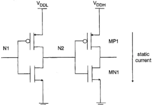
static current
Fig. 1 Direct connection of VDDL circuit and the VDDx circuit As shown in Fig. 1, the output of the V,,, circuit is directly connected to the input of the V,,, circuit. If the input node N1 of the V,,, circuit goes to low, the output node N2 then goes to high, that is V,,,. The logical high at node N2 should subsequently turn off the pull-up network MPl and turn on the pull-down network MN1. Although the voltage at node N2 is high enough to activate the NMOS MN1, it cannot cut off
the PMOS M P l due to the fact that V,,, < V,,,
I
Vlh,pl. Therefore, there exists a static current flowing directly from the applied voltage source to ground through the path of MP1 and MN1. This static currentalso consumes power so is not desirable for low power design. To avoid this unnecessary power dissipation, level converters should be placed between V,,, and
V,,, circuits. A level converter transforms a logical high produced by a V,,, circuit to the logical high for a V,,, circuit. Thus the condition that both networks
MP1 and M N l are activated at the same time as described above will not occur, and the power dissi- pated by this static current is eliminated. It should be noted that no level converter is needed in the reversed case (i.e. when the output of a V,,, circuit is con- nected to the input of a V,,, circuit).
Unfortunately, level converters consume power too. Hence a structure such as ‘VDDL circuit - V,,, circuit - V,,, circuit - V,,, circuit ...’ will need a lot of level
302
converters to be inserted at each ‘VDDL circuit - V,,, circuit’ interface. This means that the power consump- tion reduced by voltage scaling will be compensated by the extra power consumed on level converters. To avoid this problem, a CVS structure is proposed in [I]. This structure arranges all paths of a circuit in the manner ‘primary inputs - V,,, cells - V,,, cells - level converters - primary outputs’. This leads to the formation of the cluster of VD,, cells and that of VDDL
cells, as shown in Fig. 2. No level converters are needed elsewhere except at primary outputs because of
V,,, cell V,,, cell connections. The number of level converters is then minimised. The CVS structure has an additional advantage that the layout overhead is also minimised. When performing placement and routing using standard cells, one can have separate groups for the V,,, cells and the V,,, cells, respectively, and then place them in distinct rows to reduce routing over- heads.
Fig. 2 Clwtered voltage scaling structure
2.3 Basic algorithm
Assume that all the cells are initially in the V,,, ver- sion and that the timing constraints are met. In other words, the slacks of all cells are non-negative. For the gate-level netlist, backward graph-traversal is per- formed by using the depth-first-search (DFS) algorithm from the primary outputs toward the primary inputs. Each time a cell is visited, the CVS algorithm tries to replace it with its corresponding V,,, version. If the timing constraints are still met after replacement, the cell is replaced. This process is repeated until all the cells in the circuit are visited. However, if any of the slacks is detected to be negative, the replacement proc- ess at this cell is not allowed.
A couple of heuristics to determine the replacing order of candidate gates are provided. They are ‘larger C’ and ‘larger Slack’, respectively. if the heuristic ‘larger Slack‘ is chosen, the candidate nodes are sorted in descending order with their slacks. The candidate nodes are sorted in descending order with their capaci- tance when the ‘larger C’ heuristic is used. The heuris- tics are applied to the whole circuit instead of only to
primary outputs.
In performing the traversal, care should be taken when the visited cell has multiple fan-outs. When trying to replace the cells with multiple fan-outs, the forward traversal using the DFS toward the primary outputs is performed. It checks if the child cells can be replaced with V,,, cells, and is repeated until every child cell is checked.
Finally, both the V,,, cells and the VDDL cells are clustered and the CVS structure is formed.
3 Path-oriented clustered voltage scaling technique
The CVS technique assumes that a circuit is originally operating under the supplied voltage VDDH, and that it is faster than the performance requirement. Therefore, some of the gates in the circuit can be replaced with their corresponding V,,, cells so that the speed of the circuit is just above the speed needed to meet the required performance.
We can consider this problem from another point of view. Assume that the circuit is operating in the lower supplied voltage VDDL, instead of the higher voltage
V,,,. If the circuit delay still meets the performance requirement, each gate of the circuit can be in its V,,,
version. However, if the circuit delay does not meet the timing constraint, the circuit should be optimised for performance. We can replace some of the gates in the circuit with their corresponding V,,, cells to enhance the performance of the circuit (i.e. trade power for speed). However, the power being traded must be mini- mised.
We propose the PCVS technique, which adopts the point of view described above. In Section 2 we saw that the CVS technique uses the delay of the longest path to represent the delay of a circuit, and optimises the cir- cuit according to the slack information. We know that the delay of a circuit, which is equal to the delay of the longest sensitisable path, is bounded by the delay of its longest path. Therefore, the delay estimation used by the clustered voltage scaling technique is correct but pessimistic. However, if the circuit is considered to be under V,,, at the beginning, our PCVS technique can take advantage of the path sensitisation criterion and path selection criterion to identify the true critical long paths to be optimised. As the critical path is found, the delay of the circuit, which is equal to the delay of the critical path, can be more accurately calculated. More- over, as long as a set of long paths is identified, it is possible to apply the optimisation process to each selected path respectively instead of taking the whole circuit into account.
The CVS structure proposed in [1] is preferred for two different applied voltages because it minimises the number of level converters needed. Therefore our PCVS technique will adopt this circuit structure to minimise the power consumed by level converters, and we also propose a clustering algorithm to achieve this. The power reduction of a circuit optimised by the PCVS technique is better than that optimised by the CVS technique because the PCVS technique only con- siders the long sensitisable paths. We will discuss each step of the PCVS technique in detail in the following Sections.
3. I Definitions and terminology
The following definitions can be found in [2].
A combinational circuit that is bounded by primary inputs and primary outputs composes of simple gates, which are AND, NAND, OR, NOR, and NOT gates, and leads between gates. The delays of gate G and lead f a r e denoted by d(G) and d o .
A path P = (Go,
fo,
GI, f i ,...,
fm-l, G,) in a combina- tional circuit is an alternating sequence of leads and gates. Gate Go is a primary input and G, is a primary output of the circuit. LeadJ1,
0 s i s m - 1, is an on-input of P that connects gate GI and gate G i c l . A lead is called a side-input ofJ; if it is connected to G, but not
originated from Gi-l. The delay of P is the sum of the delays of all the gates and leads along P, and is denoted by dPath(P).
A controlling value to a gate G is the logic input value that independently determines the output value of G, and is denoted by c(G). For example, if one of the inputs of AND has logic value 0, the output value is determined to be 0. Therefore, the controlling value to AND is 0. A noncontrolling value to gate G is denoted by n c ( 9 , which is the complementary value of c(G).
Hence the noncontrolling value of AND is the logic value 1.
Leadf, which is connected to gate G, is said to be a
controlling input to G under the primary input vector v
if the stable value at f under v is c(G). On the other hand, f is said to be a noncontrolling input to G under v if the stable value at f is nc(G).
Let the stable value and the stable time at each input to gate G under v be unknown. Leadf, which is con-
nected to G, is considered to dominate G if the stable value and the stable time at G are determined by those at f . A path is considered to be activated by the pri- mary input vector v if each on-input of the path domi- nates the gate to which it connects. A path is defined as a sensitisable path if there is at least one primary input vector that activates the path. On the contrary, paths that cannot be activated by any primary input vector are called false paths. The critical paths are the longest sensitisable paths in the circuit.
3.2 Path selection algorithm
There are various path sensitisation criteria with differ- ent dominance definitions for the true path selection algorithms. Hence the delay estimated by using differ- ent path sensitisation criteria can have different results. Among these criteria, the exact path sensitisation crite- rion is the tightest criterion. Therefore, any other path sensitisation criterion is considered to be correct if the estimated path delay based on it is equal to or greater than the delay estimated by the exact path sensitisation criterion. As a consequence, an approximate path sen- sitisation criterion is considered to be correct if the cri- terion is looser than the exact path sensitisation criterion.
Let v be an applied primary input vector. A lead is
considered to dominate the gate to which it connects if it follows the conditions described in each path sensiti- sation criterion under the primary input vector v.
Definition 1. Exact path sensitisation criterion
A path is considered to be an exact sensitisable path if there is at least one primary input vector, such that each on-input of the path is either the earliest control- ling input or the latest noncontrolling input with all its side inputs being noncontrolling inputs too.
De$nition 2. The Brand-Iyengar path sensitisation crite- rion
A path is considered to be a Brand-Iyengar sensitisable path, it there is at least one primary input vector, such that either each on-input of the path is the lowest con- trolling input or all its side inputs are noncontrolling inputs too.
We modify the path selection algorithm proposed in
[2] by adopting the Brand-Iyengar sensitisation crite- rion for the sake of easier implementation. According to [2], a path sensitisation criterion may not be used directly as the path selection criterion. However, the
Brand-Iyengar criterion is an exception. Note that a path is considered to be a Brand-Iyengar sensitisable path, if there is at least one primary input vector such that either each on-input of the path is the lowest con- trolling input or all its side-inputs are noncontrolling inputs too. The Brand-Iyengar criterion does not sensi- tise a path by checking both the stable times and stable values of the fanins of each gate along the path. It identifies a path as sensitisable only by the geometry order of the fanins and their values. Hence during the optimisation process, the true paths selected by the Brand-Iyengar criterion will not become false paths and vice versa. Therefore, the Brand-Iyengar criterion can be used for the path sensitisation as well as the path selection.
Typically, the rising propagation delay and the fall- ing propagation delay of a gate are not equal. Other approaches using the larger of the rising and falling delays to represent the delay of a gate will surely over- estimate the delay of the circuit. In fact, the algorithm presented here can correctly handle the situation of dif- ferent rising delay and falling delay of a given gate. Therefore, the performance of a circuit estimated by this algorithm is more accurate.
The algorithm of path selection is shown in Fig. 3.
Without loss of generality the circuit being processed is assumed to have only one primary output, which is denoted by 0. For a circuit with m primary outputs, we can simply introduce a dummy primary output 0
into the circuit and then connect each original primary output to 0. It also creates a best-first-search queue (BFSQ) to perform the best-first-search algorithm from the primary outputs to the primary inputs. The algo- rithm first initialises at the dummy sink with esperance larger than the required delay z. Note that the espev-
ance of a partial path is the path delay of the longest path that contains the partial path. If the esperance of a partial path is longer than the required delay z, it means that it is possible for the partial path to expand to a complete path with the path delay longer than z.
The rising esperance is the esperance of the partial path such that its stable value is 1; while the falling esper- ance is the esperance of the partial path such that its stable value is 0. The partial path with the longest espe- rance can be found at the top of the BFSQ. If it is a
complete path it is included in the feasible set FS, and another partial path is selected from the BFSQ. Other- wise, the algorithm tries to expand the partial path with the best leadigate such that the expanded partial path is the longest untraced path. The stable value of input of the last gate is assigned to the parity of the expanded partial path. If the value is the controlling value of the last gate along the expanded partial path, all the lower side-inputs should be set to noncontrolling values. On the other hand, if the value is the noncon- trolling value of the last gate, then all the side-inputs should be set to noncontrolling values. This is based on the Brand-Iyengar criterion. The side-inputs, with their set values are included in the condition set of the expanded partial path. The leadsivalues of the condi- tion set are propagated forward and backward by the D-algorithm to verify if any inconsistency occurs. If no inconsistency is detected, the expanded partial path is inserted into the BFSQ.
3.3 Path optimisation algorithm
For each selected long path, we apply the path optimi- sation algorithm to shorten its delay. Since the circuit is optimised to have two different applied voltages, V D D H and V D D L , its performance is certainly upper bounded by the performance when the circuit is only operating under the voltage V D D H , and is lower bounded by the performance when the circuit is operating under V D D L only. Therefore, if the performance requirement of a
circuit is met when only VDDL is applied, all the gates in the circuit can surely be in their V D D L versions. Sim- ilarly, if the performance requirement of the circuit cannot be met when only V D D H is applied, the timing optimisation using CVS cannot achieve the intended goal.
Initially, all gates of the circuit are in their V D D , ver- sions. Let the selected long path be P = (Go, fo, GI, fi,
G2, f2, ...,
fm-l,
GJ, where gate Go is a primary input and G, is a primary output of the circuit. We try to optimise the path and make its delay equal to, or shorter than, the circuit delay requirement. According to the CVS structure, every single path in the circuit should be optimised to the form of ‘primary input - V D D , circuit - V D D , circuit - primary output’. In our algorithm, we cluster each path first. The whole circuitFS = Q
If the dummy sink 0 has falling esperance > T
If the dummy sink 0 has rising esperance > T
While (BFSQ is not empty)
initialise partial path ( 0 ) with parity = 0 into BFSQ; initialise partial path (0) with parity = 1 into BFSQ; Let P = (fl-l, G,, f,, . . . , 0 ) be on top of BFSQ; While (P = ( f i . l , G ; , f,, . . . , 0 ) )
If P is a complete path FS = FS U {PI;
Else
Let fi.2 be an output to Gi.l, the best remaining fan-in of Gi;
ExtP.parity = P.parity 8 parity (Gi.l);
ExtP.cond = P.cond U { [fi.l, P.parityl1;
mark fi-z as ExtP.parity; If (ExtP.parity == C(G~.~))
EXtP = (fi.2, gi.1) * P ;
For each lower side input f of f3.2
ExtP. cond = ExtP. cond U { [ f , nc (G1.]J I 1 ; Else (ExtP.parity == n c ( G , . , J )
For each side input f of fi.*
ExtP. cond = ExtP. cond U i [ f , nc (G,.,J 1 1 ; If (ExtP. cond is consistent) insert ExtP to BFSQ; If (no remaining fan-in of G, has esperance > ?)
remove P from BFSQ;
Fig. 3 Path-oriented selection algorithm with Brand-Iyengav criterion
While ( F is not empty)
Let P = ( G o , f,, . . . , Gi, F,, . . . , 0) be a path in FS;
For gates from Go to 0 along P Replace G, with its V,,, ~~ version; If the delay of P > z
Else
Replace the next gate Remove P from FS;
Fig. 4 Path optimisution algorithm
is then clustered accordingly. As shown in Fig. 4, we optimise the path by trying to replace the gates along it with their VDDH cells in order from the primary input
Go toward the primary output G,. We first replace the gate GI with a V D D H cell. if the path delay of P meets the timing constraint, the optimisation process of the path is stopped. However, if the path delay of P does not meet the timing constraint, the algorithm will try to replace the next gate G2 with its VDDH cell, and so on. The replacement process on the path P is not stopped until the timing constraint is met or the replacement reaches the primary output G,. If the performance requirement cannot be satisfied even when the whole path is operating in VDnH, the optimisation process fails.
3.4 Clustering algorithm
After the delays of all the selected paths are shortened, the circuit is guaranteed to meet the performance requirement. However after each path being clustered respectively, the whole circuit is not guaranteed to be in the CVS structure. To ensure that the circuit is clus- tered, each gate in the circuit must obey the following rule: I f a gate is selected to be replaced with a V D D H cell, all its fanin gates must also be replaced with VDDH cells.
As shown in Fig. 5, we use a breadth-first-search algo- rithm, traversing from the primary outputs toward the primary inputs, and apply the clustering rule to each gate to ensure the circuit will eventually be in the form of the CVS structure.
For all gates from G, to Go If G, is a VDz,H cell
For each fanin Gl-l of G, If is a V,,, cell)
Replace with it V,,, version;
Fig. 5 Clustering algorithm
The clustering algorithm is different from that of the CVS technique. This is because the PCVS technique
Table 1: Delay model of each gate type
does not dynamically update the gate information, as
does the CVS. Therefore, it just analyses the circuit to determine whether additional gates should be replaced with their corresponding VnDH cells. On the contrary, the CVS technique determines whether or not a gate should be replaced by using depth-first-search algo- rithm traversing from the primary inputs toward the primary outputs. Our clustering algorithm is thus more efficient.
4 Experimental results
We have implemented the path-oriented clustered volt- age scaling technique in the C language and performed the experiments on the ISCAS85 benchmark circuits on a SUN SPARC-20 workstation.
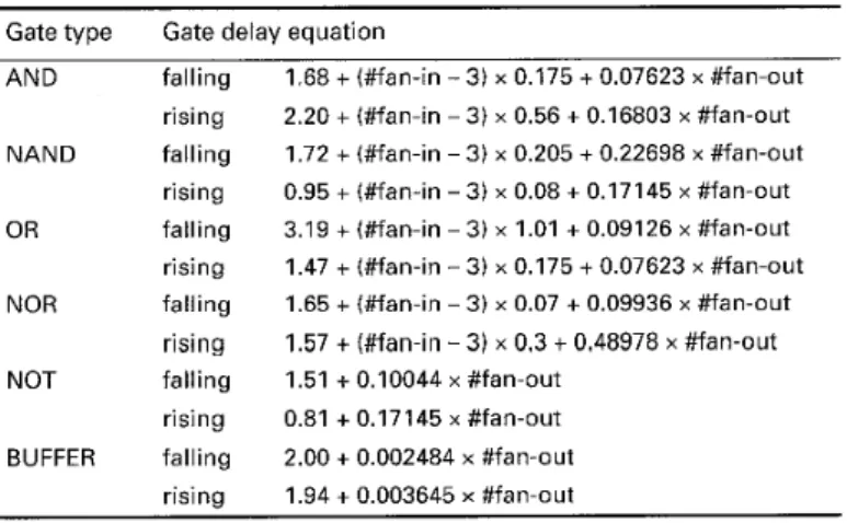
The delay model of each gate we used here is shown in Table 1. The linear model is used, and the delay of a gate is related to the number of fan-ins and fan-outs in a linear relationship. These equations are extracted from the low power LP9OOC CMOS standard-cell library of Lucent Technologies. Note that the rising and falling delay of each gate is different, which is the usual case in the real world.
We also assume the delay of a circuit is inversely pro- portional to the current flowing through it. The rela- tionship between the delay of a VDD, cell and a VDDH
cell is shown in eqn. 4.
(4)
Because the delay of a circuit is bounded by its delay in VDDH and VDDL, respectively, we divide the delay range identified by the Brand-Iyengar criterion into ten sec- tions and use the delay of each section as the required delay to optimise the circuit: e.g. if the required delay increment is 6O0/0, it means that the delay requirement
x 600/0. Therefore the circuit is optimised by both the
Of the circuit iS delayvDDH
+
(delayVDnL - delayvDDH)~~
Gate type Gate delay equation
AND falling rising falling rising falling rising falling rising rising 1.68 + (#fan-in - 3) x 0.175 + 0.07623 x #fan-out 2.20 + (#fan-in - 3) x 0.56 + 0.16803 x #fan-out 1.72 + (#fan-in - 3) x 0.205 + 0.22698 x #fan-out 0.95 + (#fan-in - 3) x 0.08 + 0.17145 x #fan-out 3.19 + (#fan-in - 3) x 1.01 + 0.09126 x #fan-out 1.47 + (#fan-in - 3) x 0.175 + 0.07623 x #fan-out 1.65 + (#fan-in - 3) x 0.07 + 0.09936 x #fan-out 1.57 t (#fan-in - 3) x 0.3
+
0.48978 x #fan-out NOT falling 1.51 + 0.10044 x #fan-out0.81 + 0.17145 x #fan-out
BUFFER falling 2.00 + 0.002484 x #fan-out 1.94 + 0.003645 x #fan-out NAND OR NOR rising 305
CVS and the PCVS techniques over the whole possible delay range.
The power of a given gate can be calculated by eqn. 5 ,
Therefore, the relationship between the power con- sumption when operating in V D D H and the power con- sumption when operating in V D D , is:
Assume the number of V D D H cells is H and the number of VDDL cells is L, the power reduction ratio can be computed by eqn. 7:
We conduct the experiment with V D O H = 5V, VDDL = 3V and Vth = 0.7V. The delay of each gate is calculated according to Table 1 and eqn. 4, and the power reduc- tion ratio can be estimated by eqn. 7.
Table 2: Experimental results of c1908
Circuit name c1908 Total number of gates 880 Circuit delay in 5V (ns)
Circuit delav i n 3V(ns) 125.80 59.99
Clustered voltage scaling technique
Number of Power reduction CPU time
(%) replaced gates ratio (%) - 0 10 - 20 - 30 - 40 37 1 50 39 1 60 395 70 402 80 484 90 538 100 586 - 26.98 28.44 28.73 29.24 35.20 39.13 42.62 < I < I < I < I < I 1 1 1 2 3 6 Path-oriented CVS technique
Number of Number Power
of replaced reduction CPU time ratio (%)
(%) paths found gates 0 347 732 10 337 321 20 319345 30 292383 40 252015 50 188 352 60 128 513 70 68 951 80 17 807 90 1042 100 0 228 372 384 486 551 641 710 774 815 863 880 16.58 27.05 27.93 35.35 40.07 46.62 51.64 56.29 59.27 62.76 64.00 3274 3202 3032 2849 2489 1910 1310 692 186 38 25 70 r
lot
O h 10 20 i o i o 50 60 7’0 80 i o l i 0required delay increment,%
Fig.6 Experimental result of e1908
-+-
cvs:-.-
PCVSThe PCVS technique can identify the false paths, as well as consider the situation with different rising delays and falling delays. Therefore, an improvement in PCVS techniques over the CVS technique is expected. Let’s use c1908 as an example for comparison first. In Table 2 and Fig. 6, we can see that the power reduction ratio of PCVS technique is much larger than that of the CVS technique over all possible delay ranges. Table 3 shows that the performance of the circuit estimated by the PCVS technique is not as pessimistic as the CVS technique. The average results of the nine benchmark circuits are shown in Table 4 and Fig. 7 over the ten delay ranges. Table 5 shows the normalised power con- sumption with respect to the original circuit, while Table 6 shows the normalised power consumption with respect to the circuit optimised by the CVS technique. We can see that the PCVS technique adds another 22% power reduction ratio on average over that of the clus- tered voltage scaling technique.
Table 3: Ratio of the highest speed estimated by the CVS and the PCVS
Hig hestSpeedcvs HighestSpeedcvs Hig hestSpeedpcvs Hig hestSpeedpcvs
~ c432 0.83 c2670 0.87 c499 0.83 c3540 0.84 c880 0.87 c5315 0.82 c1355 0.84 c7552 0.81 c1908 0.75 I
Table 4: Average experimental results
Required delay increment (%) Average power reduction ratio 0 10 20 30 40 50 - 15.013 - 22.959 6.353 30.020 21.570 34.428 29.137 40.506 33.499 44.962 cvs (%) PCVS (%) 60 36.438 51.310 70 40.910 55.990 80 44.424 59.053 90 49.733 61.154 100 53.384 64.00 Average 28.677 43.581
IEE Proc -Comput Digit Tech, Vol 145, No 4, July 1998 306
70
r
5 Conclusionsl o t
J
00 I b i o i o i o i o I30 i o 80 do IbO required delay increment,%
Fig. 7 Average experimental results
-+-
CVS; -D- PCVSTable5: Normalised power consumption with respectto the original circuit
Optimised by Optimised by
the CVS the PCVS technique technique Required delay Original
increment (%) circuit 0 1 10 1 20 1 30 1 40 1 50 1 60 1 70 1 80 1 90 1 100 1 Averaae 1 0.936 0.784 0.709 0.665 0.636 0.591 0.556 0.503 0.466 0.713 0.850 0.770 0.700 0.656 0.595 0.550 0.487 0.440 0.409 0.388 0.360 0.564
Table6: Normalised power consumption with respectto the CVS technique
Optimised by Optimised by the CVS the PCVS technique technique Required delay Original
increment (%) circuit 10 20 30 40 50 60 70 80 90 100 Averaae - 1.068 1.276 1.410 1.504 1.572 1.692 1.799 1.988 2.146 1.606 - 1 1 1 1 1 1 1 1 1 1 - 0.748 0.837 0.839 0.827 0.766 0.745 0.736 0.771 0.773 0.782
In this paper, we discussed the idea of the CVS tech- nique for low power. We then proposed the PCVS technique to improve the power reduction of a circuit. It combines the voltage scaling technique, and the long sensitisable paths identification, to achieve the CVS structure and get more power reduction. The PCVS algorithm has been verified with the ISCAS85 bench- mark circuits. The experimental results show that more gates can be voltage scaled down as compared with the CVS technique.
6 Acknowledgments
Thanks to Dr Hsi-Chuan Chen for his fruitful discus- sion and help in software development.
7 References
1 USAMI, K., and HOROWITZ, M.: ‘Clustered voltage scaling technique for low-power design’. ISLPD’95, 1995
2 CHEN, H.-C., DU, D.H.-C., and LIU, L.-R.: ‘Critical path selection for performance optimisation’, IEEE Trans., 1993, IN, H.-R., and HWANG, T.T.: ‘Dynamical identification of crit- ical paths for iterative gate sizing’. Proceedings of IEEE/ACM International Conf. on Computer-Aided Design, 1994,
CHEN, H.-C., and DU, D.H.-C.: ‘Path sensitization in critical path problem’, IEEE Trans., 1993, CAD-12, (2), pp. 196-207 DU, D.H.-C., YEN, S.H.C., and GHANTA, S.: ‘On the general false path problem in timing analysis’. Proceedings of 26th Design
automation conference, 1989, pp. 555-560
6 JONE, W.-B., and FANG, C.-L.: ‘Timing optimization by gate
resizing and critical path identification’. Proceedings of 30th
Design automation conference, 1993, pp. 135-140
7 CHANDRAKASAN, A.P., SHENG, S., and BRODERSEN, R.W.: ‘Low-power CMOS digital design’, IEEE J. Solid-State
Circ., 1992, 27, (4), pp. 473483
CIRIT, M.: ‘Transistor sizing in CMOS circuits’,Proceedings of 24th Design automation conference, 1987, pp. 121-124
DEVADAS, S., KEUTZER, K., and MALIK, S.: ‘Delay compu- tation in combinational logic circuits: theory and algorithms’. Proceedings of the IEEE ACM International Conf. on Computer-
aided design, 1991, pp. 176-179
10 GASSER, L., and HOYTE, L.: ‘Delay and power optimization in VLSI circuit’. Proceedings of the 21st Design automation confer- ence, 1984, pp. 529-535
11 PERREMANS, S., CLAESEN, L., and DEMAN, H.: ‘Static timing analysis of dynamically sensitizable paths’. Proceedings of the 26th Design automation conference, 1989, pp. 568-573 12 BRAND, D., and IYENGAR, V.: ‘Timing analysis using func-
tional analysis’. IBM Thomas J. Watson Research Centre, techni- cal report, 1986 CAD-12, (2), pp. 185-195 3 4 5 8 9 307