國
立
交
通
大
學
電機學院 電子與光電學程
碩
士
論
文
以 Alignment mark 的選擇
作為改善黃光製程上的 OVL budget 之研究
A study of Overlay Budget Improvement
by Alignment Mark Selection
研 究 生:郭宏銘
指導教授:張國明 教授
以 Alignment mark 的選擇作為
改善黃光製程上的 OVL budget 之研究
A study of Overlay Budget Improvement
by Alignment Mark selection
研 究 生:郭宏銘 Student:Hung-Ming Kuo
指導教授:張國明 Advisor:Kow-Ming Chang
國 立 交 通 大 學
電機學院 電子與光電學程
碩 士 論 文
A ThesisSubmitted to College of Electrical and Computer Engineering
National Chiao Tung University
in partial Fulfillment of the Requirements
For the Degree of Master of Science
in
Electronics and Electro-Optical Engineering
September 2010
Hsinchu, Taiwan, Republic of China
以 Alignment mark 的選擇作為改善黃光製程上的 OVL budget 之
研究
學生:郭宏銘 指導教授:張國明
國 立 交 通 大 學 電 機 學 院 電 子 與 光 電 學 程 碩 士 班
摘
要
本論文研製之始於學生在半導體製造工作有七年的經驗,工作以來全
部浸淫在黃光微影製程的環境裡。半導體黃光製程的重心一直以來都在於
線寬的縮小,眾多的論文研究無不在討論如何縮小線寬、提高解像力、增
加景深(DOF depth of focus)。所以眾多相關的技術被開發出來,例如:OPC
光罩、短波長雷射的應用、新光阻開發、泡水機(immersion)的出現。
的確在製程開發之初是線寬的縮小是個大挑戰,但是在產品到生產線
上大量生產時,與本層與前層的重合對準不佳的問題佔了每天不良貨(NG
lot)六、七成的比重。這也是學生在半導體工廠每天重複不斷遇到最多的問
題。
本篇論文是在這樣子的出發點下寫出。希望藉由對準指標(alignment
mark)與重合指標(overlay mark)的選取,來趨近實際產品的重合趨勢。以期
達到增加積體電路在本層疊對前層時的對準的能力,從而減少不良產品(NG
lot)的出現及重工(rework),提升有效產能及品質。
學生論文提出二個可能是增加重合餘裕的方法,希望能作為以後重合
指標(overlay mark)選取或者是本層前層機台間配對(machine mix matching)
的參考。
A study of Overlay Budget Improvement by Alignment Mark
selection
student:Hung-Ming Kuo Advisors:Dr. Kow-Ming Chang
Degree Program of Electrical and Computer Engineering
National Chiao Tung University
ABSTRACT
A procedure is I have worked about seven years experiment in
semiconductor manufacture. All jobs are related to the photolithography process.
The point about semiconductor photolithography process is the shrinkage of the
line pitch. Numbers of articles have been devoted to the study of how to reduce
the line pitch, enhanced the resolution, increase the DOF (depth of focus). Thus
numerous technology have been developed, example of those are: OPC (optical
proximity correction) reticle, application of short wavelength LASER,
development of new photo resist, appearance of immersion scanner. It is really a
huge challenge that shrink the line pitch at the beginning of the new
photolithography process develop, however, when the product release to the
manufacture line for mass production, there are sixty to seventy percentages of
the trouble lots is the current layer is not fine overlap to the previous layer. This
is I met the most problems in the manufacture FAB repeatedly every day.
This thesis is been written with this staring-point. I wish by the
selection of the alignment marks and overlay marks to approach the products
overlay trend for achieving an objective that increases the overlay ability of
current layer aligns previous layer. And thereupon, diminish the NG lot and lot
rework to improve the effective throughputs.
overlay margin. It is a chance to be a consult of overlay mark selection or
current layer to previous layer machine mix and matching.
誌
謝
非常感謝指導教授張國明博士三年多(首年學分班,二年半在職專班)來的指導。何 其有幸在報名學分班之初便在老師門下學習,進而引發出我考取的決心,從而在次年考 取。讓我受益良多。 謝謝口試委員成大電機系王水進教授,中華大學微電子系的賴瓊惠博士及吳建宏博 士給予我論文內容的指導。 在論文寫作的過程,同事詹孟勳、陳瀅任、張博忠、林心怡、柯奕帆給予我相當大 的幫助與鼓勵,謝謝博士班黃崧宏學長的指點,才能使這篇論文順利產生。 最後我要感謝吾妻王瑋涓的支持與鼓勵,因為你無私的奉獻家庭與小孩,我才能夠 專心致力於本論文的寫作,將此研究成果獻予吾妻以表達無限的感激。
Contents
Abstract (in Chinese) i
Abstract (in English) ii
致謝 iv
Contents v
Table Captions v
Figure Captions v
Chapter 0 Purpose and Motivation 1
0.1 An unexpected OVL improvement 1
Chapter 1 Introduction 2
1.1 The role which photolithography plays in semiconductor manufacture 2
1.2 Process sequence of photolithography 2
1.3 Process of photolithography 3
1.3.1 Primer 4
1.3.2 Resistor Coating 4
1.3.3 Soft Bake 5
1.3.4 Alignment and Exposure 5
1.3.5 PEB 7
1.3.6 Development 8
1.3.7 PDB 8
1.4 About the scanner/stepper 8
1.4.1 Scanner/ stepper 9
1.4.2 Measurement check and throughput 9
1.4.3 Resolution and DOF 10
1.5 Pattern Inspection 11 1.5.1 Defect check 11
1.5.3 OVL (overlap) check 12
Chapter 2 Theory Descriptions 14
2.1 Alignment sequence and overlay corrections 14
2.2 Measurement of the alignment mark 14
2.3 Measurement of the OVL mark 15
2.3.1 Calculation of the raw data 15
2.3.2 Wafer shift X, Y 15 2.3.3 Wafer magnification X, Y 16 2.3.4 Wafer rotation X, Y 16 2.3.5 Shot magnification 17 2.3.6 Shot rotation X, Y 17 2.4 Overlay residuals 17
2.5 Matching OVL distortion adjustment 18
2.6 Reticle and Lens heating 19
Chapter 3 Data Collection and Analysis Methods 21
3.1 Data Collection 21
3.1.1 Two layers OVL data in three months 21
3.1.2 Machine Matching Data 21
3.1.3 Process Sequence Log 22
3.2 Analysis Methods 22
3.2.1 OVL Simulation tool 22
3.2.2 Data comparison 22
3.3 Two hypotheses 22
3.3.1 Relationship between EGA mark position and distortion data 22
3.3.2 Reticle heating cause shot distortion 23
Chapter 4 Analysis 24
4.1 Simulations Matching data as EGA position 24
4.3 Reticle and projection lens heating cause shot magnification OVL data 28
4.4 The other layers verification 30
Chapter 5 Results and Conclusion 32
5.1 Results and Conclusion 32
Chapter 6 Future Work 34
6.1 Future Work 34
Table Captions Chapter 1
Table 1.1 the light source wavelength 6
Chapter 4
Table 4.1: Layer A residual XY drop after change alignment mark 24 Table 4.2: N02 simulated linear corrections and calculated residuals 26 Table 4.3: N04 simulated linear corrections and calculated residuals 27 Table 4.4: EGA measurement calculated residuals 28 Table 4.5: Layer B residual XY drop after change alignment mark 30 Chapter 5
Table 5.1: Two layers residual XY after change alignment mark in two scanner tools 30
Figure Captions Chapter 1
Fig. 1.1: sketch map of Positive and negative photo resistor 35 Fig. 1.2: The major steps of photolithography process 35 Fig. 1.4: Concept of alignment and exposure system 36
Fig. 1.5: DOF simple presence diagram 36
Fig. 1.6: KLA OVL mark 37
Chapter 2
Fig. 2.2a: Wafer shift correction 38
Fig. 2.2b: Wafer shift correction 38
Fig. 2.3a: Wafer magnification correction 39
Fig. 2.3b: Wafer magnification correction 39
Fig. 2.4a: wafer rotation correction 40
Fig. 2.4b: wafer orthogonality correction 40
Fig. 2.5: shot magnification correction 41
Fig. 2.6: shot rotation correction 41
Fig. 2.6a: concept of residual 42
Fig. 2.6b: concept of residual 42
Fig. 2.6c: concept of residual 43
Fig. 2.7: example of EGA measurement 43
Fig. 2.8: example of After EGA compensate residuals 44
Fig. 2.9: example of EGA compensation 44
Fig. 2.10: example of EGA compensation values 45
Fig. 2.11: example of OVL measurement 45
Fig. 2.12: example of after OVL compensated residuals 46
Fig. 2.13: example of OVL compensation 46
Fig. 2.14: example of OVL compensation values 47
Fig. 2.15a: N02 mix matching data in wafer map 47
Fig. 2.15b: N02 mix matching data in shot map 47
Chapter 3 Chapter 4 Fig. 4.1: N02 residuals trend chart 48
Fig. 4.2: N02 Wafer scaling XY trend chart 48
Fig. 4.3: N02 Wafer rotation trend chart 49
Fig. 4.4: N04 residuals trend chart 49
Fig. 4.6: N04 Wafer rotation trend chart 50
Fig. 4.7: N02 MM simulate KLA OVL measurement 51
Fig. 4.8: N02 MM simulate KLA OVL measurement residual 51
Fig. 4.9: N02 MM simulate KLA with 1D EGA‘s residual map 52
Fig. 4.10: N02 MM simulate KLA with 2D EGA‘s residual map 52
Fig. 4.11: N04 MM simulate KLA OVL measurement 53 Fig. 4.12: N04 MM simulate KLA OVL measurement residual 53
Fig. 4.13: N04 MM simulate KLA with 1D EGA ‘s residual map 54
Fig. 4.14: N04 MM simulate KLA with 2D EGA ‘s residual map 54
Fig. 4.15 N02 MM simulate 1D EGA ‘s map 55
Fig. 4.16 N02 MM simulate 1D EGA ‘s residual map 55
Fig. 4.17: N04 MM simulate 1D EGA ‘s map 56
Fig. 4.18: N04 MM simulate 1D EGA ‘s residual map 56
Fig. 4.19: N02 MM simulate 2D EGA ‘s map 57
Fig. 4.20: N02 MM simulate 2D EGA ‘s residual map 57
Fig. 4.21: N04 MM simulate 2D EGA ‘s map 58
Fig. 4.22: N04 MM simulate 2D EGA ‘s residual map 58
Fig. 4.23: N02 EGA_Residual_X 59
Fig. 4.24: N02 EGA_Residual_Y 59
Fig. 4.25: N04 EGA_Residual_X 60
Fig. 4.26: N04 EGA_Residual_Y 60
Fig. 4.27a: Normal (corner) and Center Shot_X OVL measurement in a lot 61
Fig. 4.27b: Normal (corner) and Center Shot_Y OVL measurement in a lot 61
Fig. 4.27c: A sketch map of Normal (corner) and Center measurement position 62
Fig. 4.28: Sketch map for center position in different magnification 62
Fig. 4.29: An axe shape shot distortion 62
Fig. 4.30: the exposure shot shape varies 63
Fig. 4.32: layer B N02 residuals trend chart 64 Fig. 4.33: layer B N04 residuals trend chart 64
Chapter 0 0.1 Motivation and Purpose
In these years I am working about the photolithography process, OVL NG takes the most energy of mine to handle it. Although most of semiconductor reference books talk about pattern resolution and DOF more. But the real situation in the manufacturing fabrication, the photolithography process engineers have to face the OVL problems more than CD or patterns NG. After shooting the OVL NG cases in these working years, as well as, I have a deeper understanding of OVL.
A case caught my attention at the year 2009. A layer’s residual dropped suddenly after change the alignment mark from 1D to 2D. The improvement is about 1~2 nm. That is a huge improvement in the 60 nm technology lithography. That means a fifteen percentage improvement of the layer to layer overlap margin is enlarged. The process margin can be loose and the yield can be improved.
Prevention is better than cure. In this thesis, I want to find out a way to make the OVL NG less before it may happen. The scanner/ stepper to scanner/ stepper have to match their lens to each other. Then the overlapping can be done. And so, the OVL NG happens.
In this thesis I bring up two hypotheses to explain the improvement of the overlay. The final purpose is to bring up a way to improvement the overlay at the alignment measurement before exposure. Then the process could run more easily.
Chapter 1 Introduction
1.1 The role which photolithography plays in semiconductor manufacture
In semiconductor manufacturing process, Photolithography is the most critical step in the process. Its purpose is to define the patterns, reduce the line pitch. Faithfully transfer the designed patterns on the mask (reticle) to the wafers is to be a mask for etching, diffusion, ion implantation. The inspections after pattern transferring include patterns, CD (Critical Dimension) size, OVL (Overlap), and defects.
It is easy to realize why the line pitch is getting narrower: the cost. Narrower line pitch means higher pattern density. It represents several things:
(1) The IC (integration circuit) which has the same functions needs the smaller area. It is smaller and lighter, so the same wafer can produce more IC. The cost is reduced, profit is brought up.
(2) We can put more electronic devices in the same area. It will have more powerful functions, a more competitive product, competitiveness is growth.
(3) The distance between electronic devices is shortened. The time which electronic signals connection to each device will be saved. Speed or frequency will be higher, competitiveness is increased.
The importance of reducing the CD size can hardly overestimate. Several observations in last few descriptions have show that the semiconductor makers try hard to shrink the line pitch. The key process of the shrinkage of the integration circuit is engineering of photolithography. The resolution and process control of engineering of photolithography have to be exact, so that they can get small enough devices on wafers.
*Reference [1],[2],[3] 1.2 Process sequence of photolithography
The key step of the whole semiconductor manufacturing is photolithography. The purpose is to define the next process step pattern on wafer. The photolithography process determinates that if the patterns can transfer to the wafer successfully or not. Supposing we cannot define out the process patterns that designer demands, then all the IC design ideas and manufacturing affairs will be just hollow words. Usually, we determine the level of process manufacturing difficulty by the order of photolithography or the number of reticles. Furthermore, can the device density of whole semiconductor go higher depends on the development of photolithography process. The most important step of the photolithography process is exposure, so every time before the exposure is made has to align, or misalignment will cause improper transferred patterns. So that the wafer can not go to next process step, it has to be reworked, it is a loss to fabrication.
*Reference [1],[2],[3]
1.3 Process of photolithography
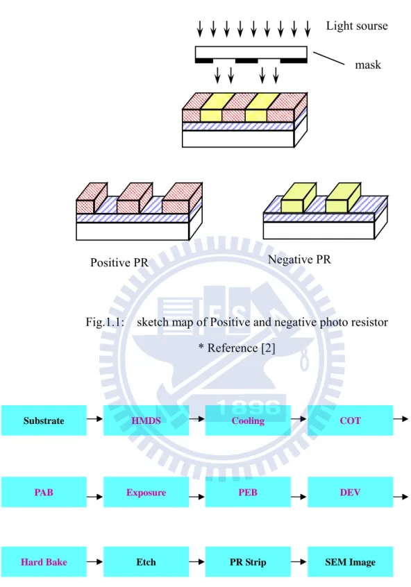
The fundamental of photolithography process is to put a layer of Photo-Sensitive Resistor on the wafer surface, usually by spinning. We call this step as PR (photo resistor) Coating. Then by using the parallel light source to irradiate through the retile with defined patterns on this Photo-Sensitive Resistor proceeds selective exposure. The light wavelength is significant to the line pitch. The wavelength is smaller; the line pitch can go narrower more easily. After exposed, the patterns on reticle are completely transferred to the photo resistor on wafer surface. We call this step as Exposure.
By the different types of photo resistors react to the light, there are two types of photo resistors. One is positive photo resistor; the other is negative photo resistor. What means positive and negative? The positive photo resistor represents that after exposure, the photo resistor can be vanish out with the area where reacted with the light by solvent developing is called positive photo resistor. On the other hand, the negative photo resistor is that when after exposure, the photo resistor is been vanish out with the area where are not reacted with the
light by solvent developing is called negative photo resistor. (See Fig. 1.1). Basically speaking, negative photo resistor is cheaper, but the resolution is worse than positive photo resistor. Opposite, the positive photo resistor is more expensive, but the resolution is better than negative photo resistor. Especially in near years, under seventy nanometer process, the photo resistor used for ArF (Argon fluoride) LASER is hundreds thousand NT dollars a gallon. The major steps of photolithography process are (see Fig. 1.2):
*Reference [1],[2],[3]
1.3.1 Primer:
Because of the silicon will oxidate with oxygen to form the silicon oxidation layer. And the chemistry characteristic of silicon oxidation layer is hydrophilic, so water may stick on the silicon oxidation layer. Nevertheless, the chemistry characteristic of positive photo resistor is hydrophobic. Therefore, it is necessary to put HMDS (Hexamethyldisilazane) on the silicon oxidation layer for increasing the adhesion between positive photo resistor and silicon oxidation layer. Due to the silicon oxidation layer is hydrophilic, steams will stick to the wafer surface. If we did not remove the wafer molecule from the surface, it is hard to make combination with HMDS and wafer surface. So before HMDS priming, it has to bake with temp about centigrade 150 for tens of seconds. We call the HMDS coating step as Priming, HMDS is the Primer.
*Reference [1],[2],[3]
1.3.2 Resistor Coating:
Nowadays photo resistor coating is to vacuum the wafer on the chuck of the resistor coater, then dispense the resistor on the wafer and spin the resistor uniformly on the whole wafer with suitable spin speed, may be one to five thousand rpm (round per minute). The spin speed depends on the requirement of the process and the characteristics of the resistor.
Although positive and negative photo resistor can be used for photolithography, but the organic solvent possesses the Swelling Effect, it is difficult to the control when the line pitch is narrower than one micrometer. So, for line pitch controlling, positive resistor much conforms to the process demand.
*Reference [1],[2],[3]
1.3.3 Soft Bake
In the process of resistor coating, when we have put the photo resistor on the wafer, it needs the second baking. We call this soft bake or pre-bake. The purpose of the soft bake or pre-bake is to drive out the most solvent of the photo resistor, besides transferring the photo resistor from liquid state to solid state. The soft bake can also increase the adhesion for the photo resistor on the wafer. After soft bake, the thickness of the photo resistor thin film might have the shrinkage about ten to twenty percentages. The baking time and temperature degree is determinate by the photo resistor types and the process requirement. If under bake, no matter lower temperature or not enough time might cause the resistor peel from the wafer. It can also influent the resolution of the pattern. Over bake might make the photo resistor get gather too early, and cause the photo resistor’s sensitivity down.
*Reference [1],[2],[3]
1.3.4 Alignment and Exposure
It is no doubt that alignment and exposure are the most important steps of the photolithography for whole IC manufacture processes. This step determinates that if we can transfer the designed patterns on the reticle to the photo resistor on the wafer successfully. The exposure process is so like to make a picture with a camera. Patterns on reticle expose to the photo resistor on the wafer just like expose the images on the camera’s negative. The difference is the resolution of exposure system of the machine that we called stepper or
scanner is much superior to the camera. And this is why the scanner or stepper is so expensive, especially the scanner. The name of stepper is come out with a machine repeats and step. Because the step can only expose one small area of the wafer once, so we need to repeat this step so many times until the whole wafer is exposed.
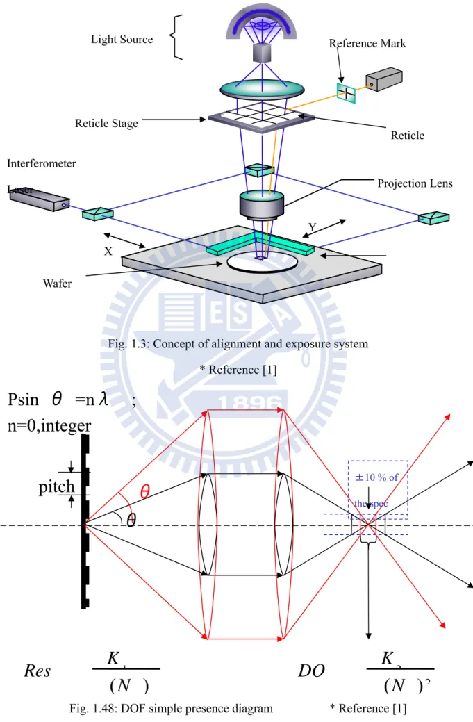
The alignment is executed for the overlay requirement. For mass production, the alignment time is the less the better; but for overlay quality, the alignment is the more the better. It needs to make a reasonable choice. Fig. 1.3 shows a sketch map of an alignment and exposure system.
The light source: In 2000s, the light sources for IC use are I-line (wavelength=365nm) emitted from the mercury lamp; DUV light, excimer LASER of KrF (krypton fluoride, wavelength=248nm) and excimer LASER of ArF (argon fluoride, wavelength=193nm). The wavelength is directly influent the narrowest line pitches. According to the Rayleigh criteria,
*Reference [1],[2]
1 2NA k
resdution EQ. 1.1 *Reference [3]
2 2NA k
DOF EQ. 1.2 *Reference [3]
We are easily able to understand the relationship between the line pitch and the wavelength. This is why nowadays photolithography process improvements are finding out a short wavelength with all developers’ strength.
*Reference [1],[2] 1.3.5 PEB
This step has different meanings to difference generation of photo resistors. The classification of the photo resistor we discussed before is positive and negative. By using different light source, the photo resistors are different. We use a CAR (chemical amplifier resistor) for DUV light sources such as KrF and ArF. Because of the excimer light power is smaller than I-line. It needs the chemical method to enhance the exposure light reacts with the photo resistor.
So, for I-line the PEB (Post Exposure Bake) is to minimize the standing wave effect of photo resistor. The standing wave effect is that when exposure light reflected from the interface of photo resistor-substrate, it produces interference with the injection exposure light and performs constructive and destructive interferences at different depth of photo resistor. The standing wave effect will perform over exposure area and under exposure area in the photo resistor layer. The main purpose of I-line photo resistor is to use the heat to make the photo resistor reflow for decreasing the dispatches of the photo resistor.
For excimer LASER CAR photo resistor, this thermal process provides the activation energy for the light acids diffuse to its suitable width for covering the insufficient of the LASER power. CAR photo resistor will release an H+ after reacting with exposure light, the H+ can make the chain effect with other non-exposure area’s photo resistor by thermal diffusion just like these non-exposure area are exposed. Then these decomposed bonding from the photo resistor will be taken out by development and the patterns are remained.
1.3.6 Development
The development removes the photo resistor where we do not need. And perform the defined reticle patterns on the wafer. For positive photo resistor, the exposure part will discompose into the developer. They usually use TMAH ((CH3)4NOH) to be the positive photo resistor’s developer. And Xylene is for the negative photo resistor use. During the development process it is necessary to keep the constant temperature or the higher temperature will cause higher chemical reaction rate. It leads to over development and CD (critical dimension) loss. On the other hand, lower temperature will cause lower chemical reaction rate. It leads to under development and incomplete development. For development process temperature control is very important for developer and wafer. Different photo resistors use different developers and different develop temperature.
*Reference [1],[2]
1.3.7 PDB
The step follows development process is PDB (post exposure bake). It is also called hard bake. Hard bake is to rid of the residual solvent in the photo resistor and increases the strength of the photo resistor by further polymerization for improving the resistance from the etching process or ion implantation. And by the thermal dehydration will enhance the adhesion between photo resistor and wafer.
*Reference [1],[2]
1.4 About the scanner/stepper
To adapt to the improvement of the process technology, the demands for resolution and precision are raising. The exposure scanner or stepper is a peculiar industry. They improve the wafer throughput per unit time and improve the resolution and DOF (depth of focus). They
have to face two difficult choice between throughput and precision; resolution and DOF. We will talk about these two situations later. First, we are going to know the concept of the scanner/stepper.
*Reference [1],[2]
1.4.1 Scanner/ stepper
Nowadays scanners using in semiconductor industry are come over a long development. The scanner is a combination of light source, illumination system, alignment system, reticle stage and wafer stage. Usually receiving wafer from the track (coater and developer) to be a photolithography machine. When exposure starts, the wafer which was coated with photo resistor is aligned by the alignment system. The light from the light source is through the reticle which was also aligned by the scanner on the reticle stage to project on the photo resistor coated wafer by the illumination system. Because of the patterns from the reticle is reduced one of quarter on the wafer by the illumination system, the wafer cannot complete the exposure by one shot exposure. It has to move to next position and exposure repeatedly to complete the whole wafer exposure. The whole exposure process is to stepping and repeat those processes, so we name it as stepper, then develop the scanner by exposure with scanning exposure.
The benefit of the scanner is the lens makers do not have to make a larger lens. The scanner is the gather area of the lens. It can easily see that it has a bigger numerical aperture. To pay for this benefit is the synchronization that wafer stage movement has to be exactly one of the quarters the reticle stage movement or the pattern transferring fails.
*Reference [1],[2]
1.4.2 Measurement check and throughput
measurement purpose is to make sure the exposure shot position and shot distortion. The messages which we call correction values or adjustment values will be sent to the scanner. According to these correction values, the scanner will adjust the wafer stage condition and lens condition to fit these corrections to make a better exposure overlap. The correction values will be discussed next section. Each scanner has its own alignment mark for measurement. Different mark, mark position, detector sensor, alignment light source all can affect the result of correction values. Although alignment measurement can make the exposure overlap better, it will sacrifice some wafer throughput. It can be easily found that if the alignment takes longer, the wafer throughput per unit time is less. This is one difficult problem to choose, better overlap and less throughput or worse overlap and more throughput. The process engineers pay huge time for this. If we have two wafer stages, then we can do exposure and alignment measurement at the same time, it seems a good solution. Unfortunately, it also has its own problem. Different wafer stages may have different stage movement characteristic. It might cause the wafer shot arrangement differences. If so, the wafers in lot may have a bigger overlap deviation.
*Reference [1],[2]
1.4.3 Resolution and DOF
To mention to resolution and DOF (depth of focus), the Rayleigh formulas are always mentioned:
1 2 NA k resdution EQ. 1.1
2 2 NA k DOF EQ. 1.2wave length can make a sharper resolution. But EQ. 1.2 told us that a larger lens numerical aperture and narrower light wave length will also shorten the focus margin, DOF. It is a more difficult problem we have to face choice. Base on the Moore’s rule: the number of transistors will be doubled and the price will be half reduced every eighteen months. The process has to choose to make bigger lens and use short wavelength ultra violet light. However, the DOF is too small to mass production without high rework rate. Fig. 1.4 shows a concept of DOF and resolution.
*Reference [1],[2]
1.5 Pattern Inspection
Inspection’s proposal is to make sure the photo resistor patterns on the wafer are no distortions, misalignment, unsuitable CD or defects on it. The photolithography processed lot will get into inspection. In general, these are three inspections to check if the exposure is good enough. These are defect check, OVL (overlap) check, CD (critical dimension) check. When a lot or wafer is disqualified by one of these inspections, the rejected product will go into the rework process. It needs to move the photo resistor and re-do the photolithography process until the lot can pass the inspections.
*Reference [1],[2]
1.5.1 Defect check
There are two ways to check the defects on the wafer. One is visual check, a coarse check. The other is to use the microscope to compare the neighbor exposure shot to find out the differences. Visual check: the operator will visual check the wafer surface and wafer back side to check large particles, defocus shots, worse coating, incomplete development, scratches, or any other obviously visual found abnormalities by human eyes. It is not a easy job to do. Because that they are working in a yellow light shined environment. Then they make use of
the OM (optical microscope) to check the patterns on the wafer surface. The check order of this step can only find the abnormalities about several ten micrometers. The defect finder machine uses for check abnormalities which human can not observe. And mark a coordinate position for human to check in SEM (scanning electron microscope) or OM more easily.
*Reference [1],[2]
1.5.2 CD (critical dimension) check
SEM is use for an inspection that patterns are smaller than 0.25 micrometer. Just like the light, light is a kind of electromagnetic waves and is a particles name photon; electron is a tiny particle and also a wave. This wave is called matter wave. The electron matter wave wavelength is determinate by the momentum of the electron.
λ=h/p EQ.1.3
It is energy mattered. The higher electron energy means the shorter wavelength. So we can put this to use high energetic electron beams to detect a tiny patterns. When the electron beam touches the target, it excites the secondary electrons. By collecting these secondary electrons, we are able to form the images of the target patterns.
The SEM check CD is to make sure that the sizes of the patterns which transferred form the reticle are suitable. Generally speaking, ten percentages CD bias of the CD target is acceptable.
*Reference [1],[2]
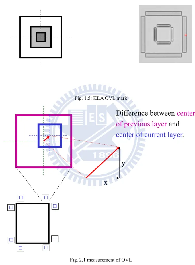
1.5.3 OVL (overlap) check
Because of the circuit device is designed as integrated circuit, the upper layer and the under layer’s overlap is extremely important. Just like the skyscraper, if the overlap is shift, the building can not be built high; the IC layer to layer overlapping is shift over the limit, the device function would not be worked.
There are many ways to measure the overlap shift between the related two layers.
In the early years of the IC fabrication, people read the vernier on wafer to know how much is the shift. The scale is about 100 nm; the error is up to 50 nm. But for the device which narrowest line pitch is about 1 micrometer that is enough.
Recently years, as the technology device designed line width goes down, the vernier reading to check overlapping shift is impracticable. The manufacturer read the overlay shift by machine measure. The KLA, measurement tools’ supplier, use box in box method to measure it. The Fig. 1.5 shows one example: box in box. Usually, we define the under layer to exposure the outer boxes, the current layer to exposure the inner ones. The tools measure the centers to each inner box to outer box for getting the shift values. The tools can also calculate the linear items of those measure values in a wafer. The linear items we will discuss each in the step chapter.
Chapter 2 Theory Descriptions
2.1 Alignment sequence and overlay corrections
All measurement is to make sure that the production is in spec what the makers define. But to make the products will be made well is more important then the measure after processing. So the machine needs to have a system to make the process well. In photolithography, one of the important systems is Alignment system.
During manufacturing, according to these OVL (overlap) raw data make some methods to compensate. Here we have two distinct types of OVL compensation. OVL-FFS (overlap feed forward system) and OVL-FBS (overlap feed back system).
The purpose of OVL-FFS (overlap feed forward system) is the lot itself. The compensation method is measure the lot before the scanner exposes. From the view of the quality control, the measurement of OVL-FFS is the more the better, but it also needs more time. However, from the view of the production, OVL-FFS measurement is the less the better.
OVL-FFS (overlap feed forward system): when the wafer before exposure the scanner will measure the exposure shot arrangement and shot distortion, the scanner vendor call this system as Alignment system. In this section, we will see the alignment sequence and the correction of the alignment.
When alignment, the scanner will measure the alignment mark get its center of it. And then compare this position to the standard mark position. So we can measure out the differences from each alignment mark. After then calculate these differences for the correction of this wafer. We will take a look on some corrections, linear corrections.
2.2 Measurement of the alignment mark
exposure procedure. After alignment measurement, the calculated correction values will send forward to the scanner/stepper to make the exposure better. With alignment, the exposure process is not a guess exposure.
The alignment sequence is: (1) wafer transfer to wafer chuck
(2) coarse alignment to get more precisely fine alignment mark position (3) fine alignment to get alignment raw data
(4) calculate and analysis the raw data to obtain the correction values (5) exposure with the correction values
The measure method is to measure the alignment mark center to compare with the given mark coordinate both X and Y direction.
2.3 Measurement of the OVL mark
After exposure, we measure the distance (or difference) from each OVL (KLA Company) marks on the wafer. It is a kind of OVL-FBS system. After measure, the correction value will send back to the control system for estimating next lot’s exposure overlay correction values to make the step up lots better.
The principle is measure the distances from the current layer’s OVL mark center to the previous layer OVL mark center. (See Fig. 2.1)
2.3.1 Calculation of the raw data
After we got all the measurement raw data, the machines, both scanner and KLA OVL machine, will compute a few linear corrections for adjustment. They may be divided into next types. We will start to know them.
The first correction to be discussed is “Wafer shift X, Y”. We can get a brief picture by Fig. 2.2ab. It is easy to calculate it. It is usually used by average all the data. Wafer shift means the average movement. The formula is also simple:
n x x x x n x X n n i i
1 1 2 3 ... EQ. 2.1Notation: Positive when X toward right, Y toward up
Negative when X toward left, Y toward down Unit: nm, μm (determinate by user)
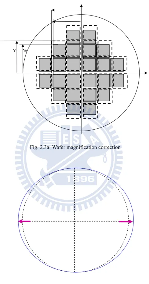
2.3.3 Wafer magnification X, Y
From Fig. 2.3ab we can easily get an image of wafer magnification X, Y. It represents the wafer scaling enlarged or reduced. It can be calculated by following formula:
Wafer scaling X = Δx / X EQ. 2.2
Notation: Positive when enlarged, Negative when reduced Unit: ppm (10-6)
2.3.4 Wafer rotation X, Y
Wafer rotation X, Y simply indicates how the wafer shots arrangement situation revolve around. (See Fig. 2.4ab) Usually we calculate as a simple equation as bellow:
Notation: Positive when Counterclockwise (right hand rule) Unit: ppm or μrad
2.3.5 Shot magnification
Refer to the Fig. 2.5, shot magnification X, Y represents the shot scaling enlarged or reduced. It can be also calculated by following formula:
Shot scaling X = ΔS_x / X EQ. 2.4
Notation: Positive when enlarged, Negative when reduced Unit: ppm(10-6)
2.3.6 Shot rotation X, Y
Shot rotation X, Y simply indicates how the wafer shots arrangement situation revolve around. (See figure 2.6) Usually it is computed as a simple equation as bellow:
Shot rotation X = ΔS_y / X EQ. 2.5
Notation: Positive when Counterclockwise (right hand rule) Unit: ppm or μrad
2.4 Overlay residuals
After alignment or overlay measurement completed, and the linear correction values have been compensated. Unfortunately, there are still some remain values can not be
compensated. We call these remain values as “overlay residuals”. Residual is the remained values (vectors) after correction. Namely, after applying all the methods to minimize the measure values, the remains are called “Residual”. The ways such as alignment measurement, OVL Feedback System … are to reduce the residual. You can say that all the overlay relative jobs are to minimize the residual to zero.
Figure 2.6a shows a example for explaining residuals. If there are only two points were measured both five nanometer, we just compensated a value negative. We can get a completely compensate picture. There are no residuals. But if the 2 measurements were measured +2 and +5 nm as the under images of figure 2.6b shows, we cannot compensate a single value to make the two values zero (the upper images of figure 2.6c shows). Otherwise, we can adjust X -3.5 nm and shot magnification as -0.2 ppm. Then we can also get a zero residual. It seems to be every value can be compensated. Theory speaking, it is possible to make the residuals zero by enough compensates. But in fact, we can not make this happened nowadays. Even if we can do this, we may pay to much time for measure and compensate these residuals. So, to keep quality and quantity’s balance, reasonable numbers of residual are allowed.
What is the reasonable numbers of residuals? It depends on the process overlap tolerances. An overlap concerned layer needs to reduced the residuals smaller more indeed. On the other hand, a non-critical layer has larger overlay budget to adopt more residuals.
2.5 Matching OVL distortion adjustment
Lens distortions do affect to the overlay. By measuring the distortion, we can get an imaging that what shape the lens distortion looks like. The method of overlay measurement is to make a reticle which has only overlay measuring boxes, the outer and inner boxes, all over the reticle.
And then exposure at first machine first time onto the wafer then develops. After develop, exposure at second machine without coating only exposure and develops with a designed
overlap shift value to make the inner boxes exposed into the outer boxes. Then we can measure box in box overlay.
Or we make an etched wafer with first machine’s exposure patterns. And use the etched wafer to collect the overlay shifts to any other machine.
According to the machine matching data we can easily to know which machine is more close to the other. The process can use this data to group the machine that the machine in a group can exchange layer to run, without run a single product at the same machine from first layer to the last.
Fig. 2.7 to Fig. 2.14 gives some examples to show the OVL and EGA (alignment) measure data and calculation results and residuals diagrams.
The machine matching data is the lens distortion information from one scanner’s lens to the Holy wafer’s differences. The Holy wafer is made by a chosen scanner or stepper which is recognized by the man. The scanner exposures patterns and then etch the pattern, so that the patterns are not able to be changed. We use these wafers to be the standards. We call these wafers as Holy wafer, Mother Wafer or Golden wafer to show its importance. We use holy wafer to know if the machine is differ from itself before or other machines. And we can use these wafers to adjust machine’s lens distortion to close itself before or make the different machine similar to each other. Fig. 2.15ab shows the tool N03 mix matching data represent in a wafer map and a shot map.
The matching data is collected to be simulated for the different position’s alignment mark measurement result. Because the matching data is measure sixty three positions in a rectangle of X 26 mm; Y 33 mm. And the alignment measurement usually measures one or two point in a shot area. So I can choose the measurement point’s measure data to approach the alignment measurement.
2.6 Reticle and lens heating
The reticle is made by glass for laser to pass though and chromium for patterns to block the light (laser). When exposure does, the glass absorbs some of exposure light. The chromium also absorbs some. The energy (laser light) can make the reticle distort, usually expansion. And the expansion is not ideally uniform. It is depend by the reticle patterns arrangement.
So does the projection lens, when the exposure light run through the projection lens, some energy left in it, it would cause lens enlarged. The variation is always unpredictable. In the later discussion, I just used the combination of reticle and lens heating’s OVL measurement data to explain the phenomenon.
Because that, in this study, I have no methods to collect separate heating data. The lens heating takes too much time to collect. It takes twelve hours to collect. It is no reason to do it for an experimental purpose. a scanner tool of half day productivity costs a big numbers of money.
Chapter 3
DATA Collection and Analysis Methods
3.1 Data Collection
3.1.1 Two layer OVL data in three months
I collected two layers OVL trend charts which were change 1D alignment mark to 2D alignment mark and both of them the residuals were improved. And I have collected two machines for comparing each other.
The data is the inline process WIP (wafer in process) which was recorded by KLA OVL measurement. Each value is fairly recorded by the fully auto measurement system. There is no artificiality in these data. And the measurement machine and recipe is critical adjusted and maintained by the professionals.
The data is too much so I make it up by the excel figures and tables for this thesis to discuss.
3.1.2 Machine matching data
I have collected the 2009 May data when is the most close to the alignment changed time.
The matching data is collected to be simulated for the different position’s alignment mark measurement result. Because the matching data is measure sixty three positions in a rectangle of X 26 mm Y 33 mm. And the alignment measurement usually measures one or two point in a shot area. So I can choose the measurement point’s measure data to approach the alignment measurement.
The data I have translated for the simulation tools use. I only put the approaching points’ data on this thesis. I have translated the matching data into 1D-EGA measurement, 2 D-EGA
measurement, and KLA OVL measure measurement for simulating.
3.1.3 Process sequence log
The process sequence log is the scanner record which recorded the exposure actions and values. I will take the reticle alignment measurement data to know how the reticle magnification is changing.
3.2 Analysis Methods
3.2.1 OVL Simulation tool
The simulation tool can simulate the alignment and OVL measurement results. And I can also use this tool to know how much the residual decrease by the linear compensation. Therefore I can know if my hypothesis is correct.
The tool is developed by the company where I work for. We use this tool to solve and analysis so many customer’s process issues. I have many confidence and experience on it.
3.2.2 Data comparison
I make use of trend charts and tables reading to description the appearance of things. And by compare the diagrams and trend charts and tables. I can get many outcomes by data comparison.
3.3 Two hypotheses
Theoretically, the measurement result is not related to the location of the EGA mark. However the real situation is the measure points in the same shot are different from each other.
So at the beginning of this case is been explained. The first thought comes out my head is: the residual goes down is due to the 2D_EGA mark position location is more similar than 1D_EGA mark to the total phenomenon of the KLA OVL measurement.
So I take the lens distortion data to imitate the EGA position and use this result to check if the residual is decreasing by the corrections of the 2D_EGA more than the 1D_EGA. The result I will description next chapter. The hypothesis is not as I have wished.
3.3.2 Reticle and projection lens heating cause shot magnification OVL data
After the failure of the previous hypothesis, I have discussed this case with teacher and classmates and colleagues. We have a thought to explain this. That is: the reticle and projection lens heating causes the shot magnification distorted. So that, the different EGA position’s EGA measurement value is affected by the shot distortion.
Due to the reticle and projection lens heating distortion, the previous layer’s patterns were exposed with distorted ones. So the EGA mark position shifts, which are why the EGA correction can give the different impact to the residuals.
Chapter 4 Analysis
4.1 Simulations Matching data as EGA position
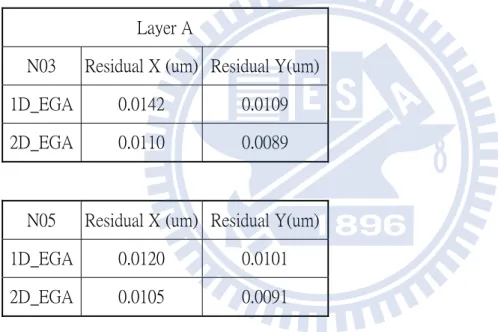
See Fig. 4.1 N03 residuals trend chart and Fig. 4.4 N05 residuals trend chart, the figure shows the residual XY have a step down from the gap, the gap is split out by the timing of the EGA mark changed. We compare the data as table 4.1.
Table 4.1: Layer A residual XY drop after change alignment mark Layer A
N03 Residual X (um) Residual Y(um) 1D_EGA 0.0142 0.0109 2D_EGA 0.0110 0.0089
N05 Residual X (um) Residual Y(um) 1D_EGA 0.0120 0.0101 2D_EGA 0.0105 0.0091
Before I simulate the mix and matching data. Let us check the wafer terms of the OVL measurement result. The Fig. 4.2 N03 Wafer scaling XY trend chart and Fig. 4.3 N03 Wafer rotation trend chart can not find out any obviously found hint. The wafer terms looks like no changes after changed the EGA mark changes. Also the Fig. 4.5:N05 Wafer scaling XY trend chart and Fig. 4.6: N05 Wafer rotation trend chart do. The wafer terms after change EGA mark of scanner tools N03 and N05 have no difference with before.
matching data to KLA OVL data. Fig. 4.8: N03 MM simulate KLA OVL measurement residual is the simulation tools calculated residuals; of course, it is divided with self calculated linear corrections.
Fig. 4.9: N03 MM simulate KLA with 1D EGA’s residual map is the simulated OVL residuals correction with 1D_EGA’s linear correction. And Fig. 4.10: N03 MM simulate KLA with 2D EGA‘s residual map is the simulated OVL residuals correction with 2D_EGA’s linear correction. It can not be found any obvious difference.
And let us check the scanner tool N05:
The Fig. 4.11: N05 MM simulate KLA OVL measurement is I simulated the mix and matching data to KLA OVL data. Fig. 4.12: N05 MM simulate KLA OVL measurement residual is the simulation tools calculated residuals; of course, it is divided with self calculated linear corrections.
Fig. 4.13: N05 MM simulate KLA with 1D EGA’s residual map is the simulated OVL residuals correction with 1D_EGA’s linear correction. And Fig. 4.14: N05 MM simulate KLA with 2D EGA‘s residual map is the simulated OVL residuals correction with 2D_EGA’s linear correction. It can not be found any obvious difference.
From Fig. 4.15 to Fig. 4.22 are the simulated 1D_EGA and 2D_EGA from scanner tools N03 and N05 EGA results and EGA residuals. These simulation are use for imitate the real EGA measurement. By using the simulation tool, I can know the variation after I key in the different correction values and the values please refer to the table 3.1 and table 3.2.
Let’s compare these data with tables. Table 3.1 and 3.2 show the linear correction values of simulated KLA, 1D_EGA and 2D_EGA with two scanner tools.
Table 4.2: N03 simulated linear corrections and calculated residuals
Linear Corrections
A B C C-A C-B
N03 1D_EGA 2D_EGA KLA 1D_EGA 2D_EGA W_shift_X -0.0051 -0.010914 -0.000223 0.004877 0.010691 W_shift_Y -0.005857 -0.001201 -0.000492 0.005365 0.000709 W_scale_X 0.029279 0.010962 0.028095 -0.001184 0.017133 W_scale_Y 0.052778 0.029545 0.031179 -0.021599 0.001634 W_Rot_X -0.001044 -0.008043 -0.037968 -0.036924 -0.029925 W_Rot_Y 0.010577 0.02875 0.034543 0.023966 0.005793 S_scale_X --- --- -0.429549 -0.429549 -0.429549 S_scale_Y --- --- -0.151899 -0.151899 -0.151899 S_Rot_X --- --- -0.105792 -0.105792 -0.105792 S_Rot_Y --- --- 0.183138 0.183138 0.183138 Residual X 0.018392 0.013075 0.012919 Residual Y 0.017249 0.015838 0.014724
Table 4.3: N05 simulated linear corrections and calculated residuals
Linear Corrections
A B C C-A C-B
N05 1D_EGA 2D_EGA KLA 1D_EGA 2D_EGA
W_shift_X -0.000678 0.003865 0.002712 0.00339 -0.001153 W_shift_Y 0.000833 0.004184 -0.001621 -0.002454 -0.005805 W_scale_X 0.158077 0.154327 0.160883 0.002806 0.006556 W_scale_Y -0.011742 -0.017298 -0.019721 -0.007979 -0.002423 W_Rot_X 0.006478 0.010039 0.026792 0.020314 0.016753 W_Rot_Y -0.00774 -0.004231 -0.019958 -0.012218 -0.015727 S_scale_X --- --- -0.085586 -0.085586 -0.085586 S_scale_Y --- --- 0.1873 0.1873 0.1873 S_Rot_X --- --- -0.192784 -0.192784 -0.192784 S_Rot_Y --- --- 0.126903 0.126903 0.126903 Residual X 0.023612 0.023617 0.023224 Residual Y 0.011594 0.008406 0.008593
We check the yellow box of the two tables, the values in table 3.1 residual_ X is 0.013075 um to 0.012919 um, residual_ Y is 0.015838 um to 0.014724 um, the residual_ X variation is minor, but the residual_ Y is changes about 1.1 nm. It is not match with the figure 3.1.
And the tools N05: from the table 3.1 residual_ X is 0.023617 um to 0.023224 um, residual_ Y is 0.008406 um to 0.008593 um, are also changing minor, less than 0.5 nm. Obviously, the EGA location’s affect is small.
Then we check the wafer terms in the table. The wafer terms values are almost no differences between 1D_EGA and 2D_EGA. However, the wafer shift XY have a obviously difference, but the average shift is not doing effect to the residual 3 sigma.
4.2 Sequence Log data compare to OVL data
Now I am going to check the EGA result residuals which were recorded when those wafer were exposure by the scanner as sequence logs.
Every tiny action on scanner will be recorded on the sequence log, including EGA measurements and calculation results.
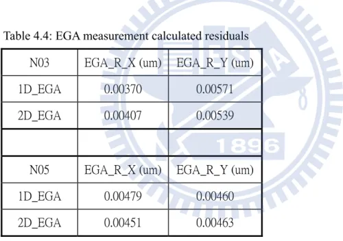
Fig. 4.23 to Fig. 4.26 show the residuals which were excluded EGA linear value by scanners, we can see that: the trend have no obviously change. Table: 4.4 can tell the value residuals before and after changing the alignment mark have no directly impact.
Table 4.4: EGA measurement calculated residuals N03 EGA_R_X (um) EGA_R_Y (um)
1D_EGA 0.00370 0.00571
2D_EGA 0.00407 0.00539
N05 EGA_R_X (um) EGA_R_Y (um)
1D_EGA 0.00479 0.00460
2D_EGA 0.00451 0.00463
4.3 Reticle and projection lens heating cause shot magnification OVL data
After checking the simulated EGA result from lens distortion data, we can hardly find strong relationship of 1D_EGA and 2D_EGA position causes the OVL residual drop.
A OVL data provides evidence for reticle and projection lens heating distortion. Figure 4.27 is one lot’s all wafers OVL measurement data. The figure 4.27a: Normal (corner) and Center Shot_X OVL measurement in a lot tells us that the center shot scaling X is about 0.15
ppm smaller than the corner measurement shot scaling X. And it is slightly getting reduced. Fig. 4.27b: Normal (corner) and Center Shot_Y OVL measurement in a lot can also tell us that the center shot scaling Y is gradually getting enlarged to the corner measurement shot scaling Y. The shot scaling Y difference is from 0 ppm to over 0.2 ppm. One may notice that the corner measurement shot scaling Y is almost keeping around 0.2 ppm.
This is an important fact to stress. Even if the corner and center shot scaling X has a gap which is about 0.2 ppm. But the gap is keep from wafer one to the last. However, the corner and center shot scaling Y is varying. I would like to emphasize that this difference cannot be found by only one point EGA measurement. This difference can only be discovered by this prepared measurement.
Is this the reason that the OVL residual dropping? This simple diagram: Fig. 4.28 helps us to realize that under the same measure point to the different magnified shot, the distance to the shot center has differences. This affects the EGA calculation.
Fig. 4.29 an axe shape shot distortion can tells us that how are the Fig. 4.27a and 4.27b looks like. The black line (middle block) is represent the standard shot we want to print out by exposure; the blue line (the wide block) represents the normal (corner) OVL measurement; the red line (the tall block) represents the center OVL measurement. And the pink axe shape figure is we use to explain the phenomenon of the residual dropped. The sketch map right side the map is the designed OVL measurement position.
According to the phenomenon which we found at Fig. 4.27, we image the exposure shape is varies like Fig. 4.30 shows. And Fig. 4.31 is the 1D_EGA mark and 2D_EGA mark designed position.
Fig. 4.30: this simple diagram seeks to capture the fact that the 1D EGA measurements is more easily to affect by the exposure shot shape distorted. According to the Fig. 4.31 the 2D_EGA mark is a comparative less affected location for EGA alignment measurement. In the case of the shot scaling X getting reduced, the explanation is the projection lens has a heating adjustment at the installation. The adjustment is a predictive correction for it. It is compensated by the number of wafer without any measurement. But there is no heating
compensation combines the projection lens and each reticle. In this case, the shot scaling X gets reduced was due to the lens heating correction value was over compensated, so that we can see the reduction of the heating situation. Oppositely speaking, the shot scaling Y gets enlarged was due to the lens heating correction value was under compensation.
And Fig. 4.31 tells us that the 2D_EGA mark is close to center than 1D_EGA is, so that the shot scaling X drifting affect the EGA measurement is smaller.
For the scanner tool, the lens area is X 26 mm, Y 7 mm, the heating affect the X more. It is one explanation of the X residual is dropped more obviously.
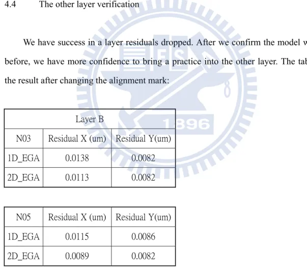
4.4 The other layer verification
We have success in a layer residuals dropped. After we confirm the model we supposed before, we have more confidence to bring a practice into the other layer. The table below is the result after changing the alignment mark:
Layer B
N03 Residual X (um) Residual Y(um) 1D_EGA 0.0138 0.0082 2D_EGA 0.0113 0.0082
N05 Residual X (um) Residual Y(um) 1D_EGA 0.0115 0.0086 2D_EGA 0.0089 0.0082
Table 4.5: Layer B residual XY drop after change alignment mark
We can also find that the layer B has the same drop phenomenon in residuals trend chart, Fig. 4.32: layer B N03 residuals trend chart and Fig. 4.33: layer B N05 residuals trend chart at
two scanner tools, especially the X direction. The layer A’s experience is successfully copied at layer B. The reason can be explained by the section 4.3.
Chapter 5 Results and Conclusion
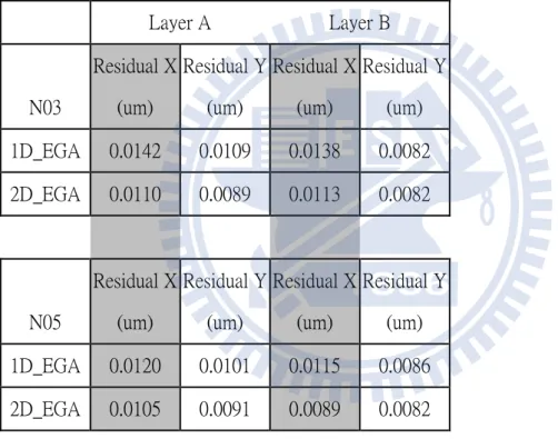
5.1 Result and Conclusion
At first, let us put the residual result in two layers at two scanner tools together, table 5.1: Table 5.1: Two layers residual XY after change alignment mark in two scanner tools.
Table 5.1: Two layers residual XY after change alignment mark in two scanner tools.
Layer A Layer B N03 Residual X (um) Residual Y (um) Residual X (um) Residual Y (um) 1D_EGA 0.0142 0.0109 0.0138 0.0082 2D_EGA 0.0110 0.0089 0.0113 0.0082 N05 Residual X (um) Residual Y (um) Residual X (um) Residual Y (um) 1D_EGA 0.0120 0.0101 0.0115 0.0086 2D_EGA 0.0105 0.0091 0.0089 0.0082
The X direction has average 19% and Y direction has average 9 % residual drop.
It is because the EGA measurement result is affected by the reticle and lens heating effect. And due to the scanner’s lens shape, a 26 x 7 exposure areas, the X direction has more effect than the Y direction does.
We suppose an axe shape distortion in section 4.3 to fit the asymmetric magnification reasonable. Reviewing the Fig. 4.29 and 4.30, we can get a simply image of the variation of
reticle and lens eating behavior. And because of the position of EGA mark located, the EGA measurement result is less affected if the mark if more close to the shot center.
The beginning thought was wrong; the position was doing less effort in the residual drop. Although the final conclusion is mark position relative, but the mark position relative is not we supposed at the beginning, the position’s distortion causes EGA measures better.
The EGA mark which more close to the center is less affected by the shot distortion, therefore, the EGA measurement result is more approach to the real situation.
Chapter 6 Future Work
6.1 Future Work
The overlay is such a huge work. It is never satisfied until the overlay controlling is perfect overlapping.
After the discussion of the OVL residuals which is seriously affected by the combination of the reticle and lens distortion. An idea comes out: if the reticle magnification compensation is useful for residual decrease, the answer should be “yes”. During these years I have more understanding of overlay. In the future, I wish I can realize more in it. And use it to improve the process margin.
Fig.1.1: sketch map of Positive and negative photo resistor * Reference [2]
Fig. 1.2: The major steps of photolithography process * Reference [2]
mask Light sourse
Positive PR Negative PR
Substrate HMDS Cooling COT
PAB Exposure PEB DEV
Hard Bake Etch PR Strip SEM Image oxide
Fig. 1.3: Concept of alignment and exposure system * Reference [1]
Fig. 1.48: DOF simple presence diagram * Reference [1]
Projection Lens Wafer Interferometer Laser X Y Reticle Stage Reference Mark Light Source Reticle
)
(
N
2K
DO
2
)
(
N
1K
Res
Psin θ =nλ ;
n=0,integer
pitch
θ
θ
±10 % of the specFig. 1.5: KLA OVL mark
Fig. 2.1 measurement of OVL
x
y
Difference between
center
of previous layer
and
Fig. 2.2a: Wafer shift correction
Fig. 2.3a: Wafer magnification correction
Fig. 2.3b: Wafer magnification correction Y Yo
Fig. 2.4a: wafer rotation correction
Fig. 2.5: shot magnification correction
Fig. 2.6a: concept of residual
Fig. 2.6b: concept of residual
+5 nm +5 nm After adjust Shift X-5nm
No
residual
+2 nm +5 nm After adjust Shift X-3.5nmResiduals
-1.5 nm +1.5 nm**Assume we can correct with only Shift X**
+2 nm +5 nm After adjust shift X -3.5 nm
residuals
-1.5 nm +1.5 nm After adjust shot scaling XNo
residual
15 mmresiduals
-1.5 nm +1.5 nmFig. 2.6c: concept of residual
Fig. 2.7: example of EGA measurement After adjust
shift X 3nm
After adjust
shift X 2 5nm
residuals
-0.5 nm -0.5 nm
**Assume we can correct with only
Shift X**
+2 nm +2 nm +4 nm +2 nm -0.5 nm +1.5 nmresiduals
-1 nm -1 nm -1 nm +1 nmWhich correction value
would be chosen?
Fig. 2.8: example of After EGA compensate residuals
Fig. 2.10: example of EGA compensation values
Fig. 2.12: example of after OVL compensated residuals
Fig. 2.14: example of OVL compensation values
Fig. 2.15a: N03 mix matching data in wafer map
0.000 0.005 0.010 0.015 0.020 0.025 1 29 57 85 11 3 14 1 16 9 19 7 22 5 25 3 28 1 30 9 33 7 36 5 39 3 42 1 44 9 47 7 50 5 53 3 56 1 58 9 61 7 64 5 67 3 70 1 72 9 75 7 78 5 Residual X Residual Y
Fig. 4.1: N03 residuals trend chart
-0.08 -0.06 -0.04 -0.02 0 0.02 0.04 1 30 59 88 117 146 175 204 233 262 291 320 349 378 407 436 465 494 523 552 581 610 639 668 697 726 755 784 -0.05 -0.04 -0.03 -0.02 -0.01 0 0.01 0.02 0.03 0.04 0.05 W_scaling X W_scaling Y
-0.03 -0.02 -0.01 0 0.01 0.02 0.03 0.04 1 30 59 88 117 146 175 204 233 262 291 320 349 378 407 436 465 494 523 552 581 610 639 668 697 726 755 784 -0.025 -0.02 -0.015 -0.01 -0.005 0 0.005 0.01 0.015 0.02 0.025 0.03 ROT_Y ROT_X
Fig. 4.3: N03 Wafer rotation trend chart
0.000 0.002 0.004 0.006 0.008 0.010 0.012 0.014 0.016 0.018 1 15 29 43 57 71 85 99 11 3 12 7 14 1 15 5 16 9 18 3 19 7 21 1 22 5 23 9 25 3 26 7 28 1 29 5 30 9 32 3 33 7 35 1 36 5 37 9 39 3 Residual X Residual Y
-0.020 -0.015 -0.010 -0.005 0.000 0.005 0.010 0.015 0.020 0.025 1 16 31 46 61 76 91 106 121 136 151 166 181 196 211 226 241 256 271 286 301 316 331 346 361 376 391 -0.04 -0.03 -0.02 -0.01 0 0.01 0.02 0.03 0.04 0.05 W_scaling X W_scaling Y
Fig. 4.5:N05 Wafer scaling XY trend chart
-0.035 -0.025 -0.015 -0.005 0.005 0.015 0.025 0.035 0.045 1 16 31 46 61 76 91 106 121 136 151 166 181 196 211 226 241 256 271 286 301 316 331 346 361 376 391 -0.045 -0.035 -0.025 -0.015 -0.005 0.005 0.015 0.025 ROT_Y ROT_X
Fig. 4.7: N03 MM simulate KLA OVL measurement
Fig. 4.9: N03 MM simulate KLA with 1D EGA‘s residual map
Fig. 4.11: N05 MM simulate KLA OVL measurement
Fig. 4.13: N05 MM simulate KLA with 1D EGA ‘s residual map
Fig. 4.15 N03 MM simulate 1D EGA ‘s map
Fig. 4.17: N05 MM simulate 1D EGA ‘s map
Fig. 4.19: N03 MM simulate 2D EGA ‘s map
Fig. 4.21: N05 MM simulate 2D EGA ‘s map
-0.02 -0.015 -0.01 -0.005 0 0.005 0.01 0.015 0.02 0.025 0.03 1 904 1807 2710 3613 4516 5419 6322 7225 8128 9031 9934 10837 EGA_R_X Fig. 4.23: N03 EGA_Residual_X -0.02 -0.015 -0.01 -0.005 0 0.005 0.01 0.015 0.02 0.025 0.03 1 904 1807 2710 3613 4516 5419 6322 7225 8128 9031 9934 10837 EGA_R_Y Fig. 4.24: N03 EGA_Residual_Y
-0.02 -0.015 -0.01 -0.005 0 0.005 0.01 0.015 0.02 0.025 0.03 1 401 801 1201 1601 2001 2401 2801 3201 3601 4001 4401 4801 5201 5601 EGA_R_X Fig. 4.25: N05 EGA_Residual_X -0.02 -0.015 -0.01 -0.005 0 0.005 0.01 0.015 0.02 0.025 0.03 1 401 801 1201 1601 2001 2401 2801 3201 3601 4001 4401 4801 5201 5601 EGA_R_Y Fig. 4.26: N05 EGA_Residual_Y
-0.5 -0.4 -0.3 -0.2 -0.1 0 0.1 S1. S2. S3. S4. S5. S6. S7. S8. S9.S10.S11.S12.S13.S14.S15.S16.S17.S18.S19.S20.S21.S22.S23.S24. Normal S_SX (ppm) Center S_SX (ppm)
Fig. 4.27a: Normal (corner) and Center Shot_X OVL measurement in a lot
0 0.1 0.2 0.3 0.4 0.5 S1. S2. S3. S4. S5. S6. S7. S8. S9.S10.S11.S12.S13.S14.S15.S16.S17.S18.S19.S20.S21.S22.S23.S24. Normal S_SY (ppm) Center S_SY (ppm)
Fig. 4.27b: Normal (corner) and Center Shot_Y OVL measurement in a lot
Fig. 4.27c: A sketch map of Normal (corner) and Center measurement position
Fig. 4.28: Sketch map for center position in different magnification
Fig. 4.30: the exposure shot shape varies
Fig. 4.31: 1D_EGA mark and 2D_EGA mark designed position
Wafer 1 Wafer 2
0. 0.002 0.004 0.006 0.008 0.01 0.012 0.014 0.016 0.018 0.02 1 32 63 94 125 156 187 218 249 280 311 342 373 404 435 466 497 528 559 590 621 Residual X Residual Y
Fig. 4.32: layer B N03 residuals trend chart
0. 0.002 0.004 0.006 0.008 0.01 0.012 0.014 0.016 0.018 1 49 97 145 193 241 289 337 385 433 481 529 577 625 673 721 769 817 865 913 Residual X Residual Y
Reference Documents
[1] 蕭宏,半導體製程技術到論修訂版,歐亞書局有限公司,民國 96 年
[2] 力晶半導體,新進工程師訓練手冊,民國 94 年

![Table 1.1 the light source wavelength * Reference [1]](https://thumb-ap.123doks.com/thumbv2/9libinfo/8101960.165224/18.892.150.822.516.1124/table-light-source-wavelength-reference.webp)