規則化量子點晶格及半導體量子環之研究
121
0
0
全文
(2) 規則化量子點晶格及半導體量子環之研究. Ordered Quantum Dots Lattice Growth and Studies of Semiconductor Quantum Rings 研 究 生 :李 秉 奇 指導教授 :李 建 平 博 士. Student : Bing-Chi Lee Advisor : Dr. Chien-Ping Lee. 國 立 交 通 大 學 電子工程學系電子研究所 博 士 論 文 A Dissertation Submitted to Department of Electronics Engineering College of Electrical Engineering and Computer Science National Chiao Tung University in Partial Fulfillment of the Requirements for the degree of Doctor of Philosophy in Electronics Engineering June 2004 Hsinchu, Taiwan, Republic of China. 中華民國九十三年六月.
(3) 規則化量子點晶格及半導體量子環之研究. 學生: 李秉奇. 指導教授: 李建平 博士 國立交通大學 電子工程學系 電子研究所. 摘. 要. 本論文由兩個部分組成,規則化量子點晶格成長與量子環結構之研究。 有關第一部份,我們提出了利用格式化基板之選擇性成長方法來達成控制量子點 之位置和數目並以實驗證明﹔在另一部份中,自組式半導體量子環結構之成長與 特性是討論的主題。 關於量子點之選擇性成長,本論文使用兩種不同之格式化基板方法。首 先,我們使用電子束微影和溼式蝕刻形成不同之圖案,並利用原子在不同晶面上 所展現之特性,來製作出具有完整晶格結構和長程規則排列之一維量子點陣列。 尤有甚者,我們更發展出一種利用應變累積方式,來達成單一量子點之成長。利 用這種技術,我們成功地製作出二維規則排列之單一量子點晶格。 接著,我們詳細地探討了在(100)砷化鎵基板上自組式半導體砷化銦鎵 量子環的研究與成長。利用 AFM 量測,我們個別探討了四個主要長晶參數,砷 化鎵覆蓋層之長晶速率,砷化鎵覆蓋層之基板溫度,退火溫度與退火時間。我們 發現 dewetting 過程是量子環形成之主要原因,而擴散作用則嚴重地影響量子環 之表面型態和組成分怖。此外,為了解決以傳統方式成長量子環,須仔細考慮成 長條件之缺失,我們提出了以擴散位障為基礎之方法,藉由額外加入一層 AlAs 來阻止鎵原子向內擴散而和銦原子形成合金,因而可以在較為寬鬆之成長條件之 下製作出量子環。. i.
(4) Ordered Quantum Dots Lattice Growth and Studies of Semiconductor Quantum Rings Student: Bing-Chi, Lee. Advisor: Dr. Chien-Ping, Lee. Department of Electronic Engineering and Institute of Electronic Engineering National Chiao Tung University. Abstract This dissertation consists of two parts: ordered quantum dots lattice growth and semiconductor quantum rings structures. In the first part, selective growth methods on patterned substrates to achieve position- and number-controlled self-assembled quantum dots were proposed and demonstrated experimentally. In the second part, the growth and characterization of self-assembled semiconductor quantum rings were discussed. As regards QDs selective growth, two approaches of patterned substrates were used in this dissertation. First of all, a high quality crystalline and long-range ordering of QDs array was obtained by making use of different migration behaviors on the faceted surface generating by e-beam nanolithography and wet chemical etching. Besides, a new technique based on strain accumulation was developed for achieving single QDs fabrication. Using this method, 2D ordered single QDs lattice have been demonstrated. In the following, studies and fabrication of self-assembled semiconductor In(Ga)As quantum rings on (100) GaAs substrate were discussed in detail. Using AFM measurements, four main growth parameters, GaAs capped growth rate, GaAs capped. ii.
(5) temperature, annealing temperature and annealing time, have been studied and discussed respectively. We found that the dewetting process is the dominant mechanism in the formation of quantum rings, and the diffusion-driven transformation greatly influences the surface morphology and composition distribution. Furthermore, a new growth technique based on the diffusion barrier method was developed to solve the problem that the fabrication of quantum rings is strongly dependent on the growth conditions traditionally. An additional AlAs layer impedes the inward diffusion of the Ga and Al atoms and results in nano-ring formation with a more relaxed growth condition.. iii.
(6) 誌. 謝. 由衷的感謝李建平教授多年來的指導,老師敏銳的思考,豐富的學養,以及 嚴謹的治學,引導我進入 Science 這個美麗殿堂,此外,老師為實驗室爭取到充 裕的研究資源,使我們在作學問時,毫無後顧之憂,在此致上最深切的謝意。 另外還要感謝高中時期的導師徐正梅老師。當年他對我們的期許:一個優秀 的理工人材,還需具備豐富的人文素養。這個教誨改變了我的一生,讓我沉浸在 科學研究之餘,更能享受文學藝術之美。 對於 MBE 研究群,特別感謝多位畢業學長:劉德成博士、吳正信博士、曾 堅信博士、蔡嘉明博士、范振權博士、顏順通博士、蔡富義博士、王祥宇博士、 林國瑞博士、以及林聖迪博士,在諸多困境中,你們適時的給予支援,使我能順 利突破困境。還要感謝所有的實驗室成員:林志昌、李建騏、王興燁、廖志豪、 黃世傑、羅明城、張至揚、黃博聲、呂佳穎,和碩一學弟楊仁盛、王勝雄、凌鴻 緒、陳力輔,每當我研究碰到低潮時,各位學弟妹的支持與鼓勵,是我繼續勇往 直前的力量泉源。 非常感謝生我鞠我,長我育我的雙親。在我的成長與求學過程,您們費盡思 量,對於我的選擇與決定,更是堅定的支持和默默的包容。您們無悔的付出,才 有今日的我。我愛您們! 謹以此論文獻給所有關心我的長輩和好友。. iv.
(7) CONTENTS. Abstract (Chinese). i. Abstract (English). ii. Acknowledgement. iv. Contents. v. Table captions. viii. Figure captions. ix. Chapter 1: Introduction 1.1 Ordered quantum dot lattices. 1. 1.2 Studies of semiconductor quantum rings. 3. 1.3 Organization of dissertation. 3. References for chapter 1. 5. Chapter 2: Experimental techniques 2.1 Molecular beam epitaxy growth. 9. 2.2 Material characterization. 14. References for chapter 2. 18. Chapter 3: InAs/GaAs quantum dots growth and characterization 3.1 Introduction to QDs fabrication. 26. 3.2 Self-assembled InAs/GaAs QDs growth by MBE. 28. 3.3 Growth conditions of self-assembled InAs/GaAs QDs. 30. 3.4 Summary. 34 v.
(8) References for chapter 3. 35. Part A. Ordered Quantum Dots Lattice Growth Chapter 4: Selective growth of InAs quantum dots array on patterned GaAs (001) substrates 4.1 Introduction. 51. 4.2 Experiments. 53. 4.3 Results and discussion. 54. 4.4 Summary. 56. References for chapter 4. 57. Chapter 5: Selective growth of single quantum dots 5.1 Introduction. 66. 5.2 Experiments. 67. 5.3 Sample characterization and results. 69. 5.4 Summary. 70. References for chapter 5. 71. Part B. Studies of semiconductor quantum rings Chapter 6: Studies of semiconductor quantum rings Part I: formation mechanism 6.1 Introduction. 78. 6.2 Experiments and discussion. 81. 6.3 Summary. 83. vi.
(9) References for chapter 6. 84. Chapter 7: Studies of semiconductor quantum rings Part II: fabrication using GaAs/AlAs capped layer 7.1 Introduction. 92. 7.2 Experiments and discussion. 93. 7.3 Summary. 96. References for chapter 7. 97. Chapter 8: Conclusion and future works 8.1 Conclusion of present studies. 103. 8.2 Future works. 105. Vita Publication List. vii.
(10) Table captions Table 3.1 InAs QDs growth parameters. Table 6.1 Growth conditions of quantum rings. viii.
(11) Figure captions Fig. 2.1 A schematic of our Varian Gen II MBE system. Fig. 2.2 One of measured RHEED oscillations in our system. Fig. 2.3 One of calibrated plots for growth rate and beam flux equivalent pressure. Fig. 2.4 A schematic of the PL measurement system. Fig. 2.5 MultiMode SPM (upper image) and optical head (lower image). Fig. 2.6 AFM images of QDs in the same sample taken with different tips. Fig. 2.7 The relations between the amplitude (phase) and oscillation frequency of the cantilever. Fig. 2.8 The amplitude (phase) shift at the fixed frequency due to the tip-sample interaction. Fig. 3.1 Fabrication procedure of ‘thermal etching’ quantum dots. Fig. 3.2 Growth procedure for InAs/GaAs QDs in S-K mode. Fig. 3.3 Three growth modes in heterostructure epitaxy, Frank-van der Merwe (F-M), Volmer-Weber (V-W), and Stranski-Krastanow (S-K).. Fig. 3.4 A typical sample structure of InAs QDs growth, the top InAs QDs are used in AFM measurement. Fig. 3.5 AFM images of uncapped InAs QDs. Fig. 3.6 The PL spectrum of grown InAs/GaAs QDs measured under different excitation powers Fig. 3.7 The surface morphology of uncapped InAs QDs using a mixture of As2/As4 vapor (on condition that a high V/III ratio is used during InAs deposition) Fig. 3.8 The surface morphology of uncapped InAs QDs using a mixture of As2/As4 vapor (on condition that a low V/III ratio is used during InAs deposition) Fig. 3.9. The PL spectrum of grown InAs QDs using a mixture of As2/As4 vapor. ix.
(12) (a) with a high V/III ratio , (b) with a low V/III ratio during InAs deposition Fig. 3.10 The PL spectrum of grown InAs QDs under different capped growth rate (using a mixture of As2/As4 vapor). (a) 1µm/hr, (b)0.3µm/hr Fig. 3.11 The PL spectrum of grown InAs QDs (without growth interruption) Fig. 3.12 The PL spectrum of grown InAs QDs (with growth interruption) Fig. 4.1 (a) Two types of square grids patterns with pitch of 0.1µm, (b) SEM images of the patterns after the wet chemical etching Fig. 4.2 The TEM image of the uncapped QDs on the non-patterned area (in the upper half of the figure) and pattern B (in the lower half part). Fig. 4.3 The AFM images of QDs grown on the pattern A. The inset shows a single row of dots that formed on the mesa stripes Fig. 4.4 The AFM images of QDs inside the pits of pattern A. The inset also shows one single row of dots sited against one of the sidewalls. Fig. 4.5. The TEM image shows that dots formed on the ridge and valley, which is consistent with the AFM image Fig. 4.6 The TEM image shows that dots formed inside the pits only and no dot landed on the mesa top Fig. 4.7 The PL spectra of the QDs sample are taken from three different areas: pattern A, non-patterned area, and pattern B. Fig. 5.1 Four sample structures designed for single QDs studies Fig. 5.2 Flow diagram of a selective growth of single QDs. Fig. 5.3 (a) SEM image of mesa lattice after MBE regrowth, (b) AFM image of mesa lattice with QD formed on the top of mesa, and (c) the surface profile across a mesa and a single QD. Fig. 5.4 TEM image shows the strain field on the mesa changes fundamentally due to. x.
(13) formation of single QD Fig. 5.5 TEM image shows a 2D ordered single QDs lattice fabricated by strain accumulation Fig. 6.1 A schematic of quantum rings formation in the diffusion-driven transformation Fig. 6.2 A schematic of quantum rings formation in the dewetting model Fig. 6.3 The AFM image of grown QDs shows twofold distributions in size. Fig. 6.4 The surface morphology of quantum rings with different growth conditions. Fig. 6.5 The phase shift of quantum rings with different growth conditions Fig. 6.6 The alloying effect on quantum rings formation Fig. 7.1 AFM images showing the surface morphology of quantum rings formed with different GaAs/AlAs cap layers. The thickness of GaAs/AlAs is (a) 0Å/25Å, (b) 5Å/20 Å, (c) 10Å/15 Å, (d) 15Å/10Å and (e) 0Å/25Å. Fig. 7.2 AFM images of quantum rings capped with 20ÅGaAs/ 5Å AlAs. (a) without thermal annealing, (b) with increasing temperature by 10oC in one minute and then maintaining for 2 minutes. Fig. 7.3 The plan-view TEM image shows that the shape and strain distribution of quantum rings Fig. 7.4 A schematic of quantum rings formation with GaAs/AlAs partial capped layers.. xi.
(14) Chapter 1 Introduction. The development of the physics and technology of semiconductor heterostructures have brought about enormous changes in our daily lives [1.1]. Heterostructure-based electronic devices have been widely used in many areas [1.2-1.4]. For example, optoelectronic devices such as laser diodes, photodetectors and modulators, have been applied in optical communication, optical storage/readout, optical interconnect, and image capture/display. As for researches on fundamental physics experiments, two-dimensional electron gas (2DEG) with very high electron-mobility in GaAs/AlGaAs system has provided a good candidate for various scientific studies [1.5-1.10]. Moreover, in the 1990s, a great breakthrough in semiconductor heterostructures is related to the fast development of the new classes of structures—self assembled quantum dots (QDs) [1.11-1.13]. Nowadays, advanced growth techniques such as molecular beam epitaxy (MBE) and metal organic vapor phase epitaxy (MOVPE) have allowed us to produce a diversity of semiconductor nanostructures with different geometries, which are precise on atomic scale and in which the carrier motion is confined in one, two and three spatial directions. Two subjects are addressed in this dissertation: one is about ordered quantum dots lattice growth and the other is about fabrication and material characterization of quantum rings.. 1.1 Ordered quantum dot lattices Nanostructures based on semiconductors have received much attention of physicists and technologists due to their novel quantum effects [1.14-1.15]. Especially. 1.
(15) for QDs, they resemble an atom. These nanoscale structures with spatially limited carriers in all three dimensions realize size quantization in semiconductor and modify the electronic and optical properties of the systems [1.16]. Although many novel characteristics about 0-D quantum structures in semiconductors have been predicted for a long time, the realization has to wait for an appropriate method for their fabrication. Of the many techniques proposed and investigated for the fabrication of QDs, the most promising one is that of self-assembled growth. In heteroepitaxial systems, pyramidal-shaped QDs can be formed by the Stranski-Krastanow (SK) transition at early stage of the strained growth [1.13, 1.17-1.18]. Unlike the prior fabrication methods, which were suffered from the serious surface defects problem, the self-assembled QDs have demonstrated advantages of high-quality, defect-free properties and ease of fabrication. Owing to their superior optical and electronic properties, several kinds of optoelectronic devices using the self-assembled QDs as their active medium have exhibited good performances [1.19-1.22]. However, the QDs grown using the S-K growth mode are usually randomly distributed on the grown surface and suffer from fluctuations of sizes and strain in a random manner. It is almost impossible to place the QDs in a regular way or on the designated locations. The size fluctuation also results in large inhomogeneous broadening in their energy spectrum. These seriously limit the potential device applications of such QDs. So far, several types of strategies have been developed to overcome deficiencies derived from S-K growth mode. Roughly, these strategies can be classified into two categories: (a) patterned substrate methods that make use of selective growth on the surface [1.23-1.31], and (b) strain engineering methods based on introducing a built-in anisotropic strain distribution in the surface [1.32-1.35].. 2.
(16) 1.2 Studies of semiconductor quantum rings Microscopic and mesoscopic metallic and semiconductor quantum rings have attracted much interest due to the occurrence of persistent currents when the systems are threaded by magnetic fields [1.36-1.38]. This phenomenon is related to Aharonov-Bohm effect, which is a direct consequence of the ring topology. Recently, advanced growth techniques have made it possible to produce semiconductor quantum ring in a single growth run [1.39-1.42]. The self-assembled quantum rings are considered as the best candidate to exhibit various phenomena related to ring topology due to their scattering-free and few-particle limit properties. Owing to their high quality, the InAs quantum rings have attracted much interest and were studied widely using various methods, including optical and electrical methods [1.15, 1.43-1.47]. Such experimental results provide undoubted evidence that the nanoscale surface ring-shaped morphology is able to exhibit quantum mechanical properties with rotational symmetry. In addition to studies on various optical and electrical properties of InAs quantum rings, the growth technique and formation mechanism are also the subjects of major research interest. Two of mechanisms were proposed to explain the shape transformation from dots to rings: one is based on kinetic consideration; the other is based on thermodynamic consideration [1.39-1.41, 1.48]. It is believed that these two mechanisms contribute to the formation of the quantum rings.. 1.3 Organization of dissertation This dissertation is classified into two subjects. The first subject is concerned with ordered quantum dot lattices growth and the other is with quantum ring-like nanostructures. Before getting into the main subjects, the experimental techniques used. 3.
(17) in this dissertation are described in chapter 2. In the following, the growth condition dependence and characterization of QDs are studied in chapter 3. As for the first subject of this dissertation, the studies with ordered quantum dot lattices growth are presented at first. A chain of ordered quantum dot array formed on the GaAs (100) substrate patterned by electron beam nanolithography. Next, a new technique was developed to position a single QD on a predesigned location to improve device applications. In the second subject, fabrication method and formation mechanism of In(Ga)As semiconductor quantum rings are discussed. Then, a new growth method to produce quantum rings is proposed and demonstrated experimentally. Finally, a conclusion and a brief description in the future works are presented.. 4.
(18) References. [1.1] J. Singh, Physics of semiconductors and their heterostructures, McGRAW-Hill, Inc. international editions, (1993) [1.2] S. L. Chuang, Physics of optoelectronic devices, John Wiley & Sons, Inc., New York, (1987) [1.3] D. Dragoman and M. Dragoman, Advanced optoelectronic devices, Springer, New York, (1999). [1.4] M. Fukuda, Optical semiconductor devices, John Wiley & Sons, Inc., (1999) [1.5] J. H. English, A. C. Gossard, H. L. Störmer, and K. W. Baldwin, Appl. Phys. Lett. 50, 1826 (1987). [1.6] M. Shayegan, V. J. Goldman, C. Jiang, T. Sajoto, and M. Santos, Appl. Phys. Lett. 52, 1086 (1988). [1.7] L. Pfeiffer, K. W. West, H. L. Störmer, J.P. Eisenstein, K. W. Baldwin, D. Gershoni and J. Spector, Appl. Phys. Lett. 56, 1697 (1990). [1.8] D. C. Tsui and H. L. Störmer, J. Quantum Electron. 22, 1711 (1986). [1.9] H. L. Störmer, D. C. Tsui, and A. C. Gossard, Rev. Mod. Phys 71, S298 (1999) [1.10] H. L. Störmer, Rev. Mod. Phys 71, 875 (1999) [1.11] L. Goldstein, F. Glas, J. Y. Marzin, M. N. Charasse and G. Le Roux, Appl. Phys. Lett. 47, 1099 (1985). [1.12] D. Leonard, M. Krishnamurthy, C.M. Reaves, S.P. Denbaars, and P.M. Petroff, Appl. Phys. Lett. 63, 3203 (1993) [1.13] W. Seifert, N. Carlsson, M. Miller, M. Pistol, L. Samuelson, and L. R. Wallenberg, Prog. Crystal Growth and Charact. 33, 423 (1996). [1.14] Y. Arakawa and H. Sakaki, Appl. Phys. Lett. 40, 939 (1982). 5.
(19) [1.15] A. Lorke, R. J. Luyken, A. O. Govorov, and J. P. Kotthaus, Phys. Rev. Lett. 84, 2223 (2000). [1.16] M. Grundmann, J. Christen, N. N. Ledentsov, J. Böhrer, D. Bimberg, S. S. Ruvimov, P. Werner, U. Richter, U. Gösele, J. Heydenreich, V. M. Ustinov, A. Yu. Egorov, A. E. Zhukov, P. S. Kop'ev, and Zh. I. Alferov, Phys. Rev. Lett. 74, 4043 (1995) [1.17] J. Y. Tsao, Materals fundamentals of molecular beam epitaxy, Academic press, Inc. (1993) [1.18] W.K. Liu and M.B. Santos, Thin films: heteroepitaxial systems, World Scientific, (1999) [1.19] N. Kirstaedter, N. N. Ledentsov, M. Grundmann, D. Bimberg, V. M. Ustinov, S. S. Ruvimov, M. V. Maximov, P. S. Kop’ev, Zh. I. Alferov, U. Richter, P. Werner, U. Gosele, and J. Heydenreich, Electron. Lett. 30, 1416 (1994). [1.20] S.K. Jung, C. K. Hyon, J. H. Park, S. W. Hwang, D. Ahn, M.H. Son, B. D. Min, Yong Kim, and E. K. Kim, Appl. Phys. Lett.75, 1167 (1999). [1.21] G.. Yusa, and H. Sakaki, Electron. Lett, 32, 491 (1996). [1.22] S. Y. Wang, S. D. Lin, H. W. Wu and C. P. Lee, Appl. Phys. Lett. 78, 1023 (2001). [1.23] D. S. L. Mui, D. Leonard, L.A. Coldren, and P. M. Petroff, Appl. Phys. Lett. 66, 1620 (1995). [1.24] M. Kitamura, M. Nishioka, J. Oshinowo, and Y. Arakawa, Appl. Phys. Lett. 66, 3663 (1995). [1.25] R. Zhang, R. Tsui, K. Shiralagi, D. Convey, and H. Goronkin, Appl. Phys. Lett. 73, 505 (1998). [1.26] C. K. Hyon, S. C. Choi, S.-H. Song, S. W. Hwang, M. H. Son, D. Ahn, Y. J. Park and E. K. Kim, Appl. Phys. Lett. 77, 2607 (2000).. 6.
(20) [1.27] Cheol-Koo Hahn, Junichi Motohisa, and Takashi Fukui, Appl. Phys. Lett. 76, 3947 (2000). [1.28] Hyo Jin Kim, Junichi Motohisa, and Takashi Fukui Appl. Phys. Lett. 81, 5147 (2002). [1.29] B. H. Choi, C. M. Park, S.-H. Song, M. H. Son, S. W. Hwang, D. Ahn, and E. K. Kim, Appl. Phys. Lett,78, 1403 (2001). [1.30] S. C. Lee, L. R. Dawson, K. J. Malloy, and S. R. J. Brueck, Appl. Phys. Lett. 79, 2630 (2001). [1.31] X. Mei, D. Kim, H. E. Ruda,and Q. X. Guo, Appl. Phys. Lett. 81, 361 (2002). [1.32] H. Lee, J. A. Johnson, M. Y. He, J. S. Speck, and P. M. Petroff, Appl. Phys. Lett. 78, 105 (2001). [1.33] T. Mano, R. No¨ tzel, G. J. Hamhuis, T. J. Eijkemans, and J. H. Wolter, Appl. Phys. Lett, 81, 1705 (2002). [1.34] Kwang Moo Kim, Young Ju Park, Young Min Park, Chan Kyeong Hyon, Eun Kyu Kim, and Jung Ho Park, J. Appl. Phys. 92, 5453 (2002). [1.35] T. Mano, R. No¨ tzel, G. J. Hamhuis, T. J. Eijkemans, and J. H. Wolter, J. Appl. Phys. 95, 109 (2004). [1.36] L. P. Lévy, G. Dolan, J. Dunsmuir, and H. Bouchiat, Phys. Rev. Lett. 64, 2074 (1990). [1.37] V. Chandrasekhar, R. A. Webb, M. J. Brady, M. B. Ketchen, W. J. Gallagher, and A. Kleinsasser, Phys. Rev. Lett, 67, 3578 (1991). [1.38] D. Mailly, C. Chapelier, and A. Benoit, Phys. Rev. Lett. 70, 2020 (1993). [1.39] A. Lorke, R. Blossey, J. M. García, M. Bichler, and G. Abstreiter, Mater. Sci. Eng. B 88 225 (2002) [1.40] T. Raz, D. Ritter, and G. Bahir, Appl. Phys. Lett, 82 1706 (2003). 7.
(21) [1.41] D. Granados, and J. M. García, Appl. Phys. Lett. 82 2401(2003). [1.42] J. Cui, Q.He, X. M. Jiang, Y. L. Fan, X. J. Yang, F. Xue and Z. M. Jiang, Appl. Phys. Lett. 83 2907(2003) [1.43] A. Lorke, and R. J. Luyken, Physica B 256-258 424(1998) [1.44] H. Pettersson, R. J. Warburton, A. Lorke, K. Karrai, J. P. Kotthaus, J. M. García, and P. M. Petroff, Physica E 6 510 (2000) [1.45] A. Emperador, M. Pi, M. Barranco, and A. Lorke, Phys. Rev. B 62 4573 (2000) [1.46] R. J. Warburton, C. Schäflein, D. Haft, F. Bickel, A. Lorke, K. Karrai, J. M. García, W. Schoenfeld, and P. M. Petroff, Physica E 9 124(2001) [1.47] R. J. Warburton, C. Schulhauser, D. Haft, C. Schäflein, K. Karrai, J. M. García, W. Schoenfeld, and P. M. Petroff, Phys. Rev. B 65 113303(2002) [1.48] R. Blossey, and A. Lorke, Phys. Rev. E 65 021603(2002). 8.
(22) Chapter 2 Experimental techniques. In this chapter, the experimental techniques used in these studies are presented. They mainly consist of two parts: sample growth and material characterization. All the samples were grown with the molecular beam epitaxy (MBE) system in our laboratory. The material characterization techniques are stated in the last section of the chapter: photoluminescence and atomic force microscope. The concise setups and basic operating principles of measurement instruments are described briefly here.. 2.1 Molecular beam epitaxy growth [2.1-2.3]. 2.1.1 Introduction to our MBE system Basically, molecular beam epitaxy (MBE) is a vacuum evaporation technique defined as the growth of epitaxial films onto the heated substrates using atomic and molecular beams produced from Kundsen effusion cells (K-cell) under ultra-high vacuum condition. It is a physical deposition, which is carried out under condition far from thermodynamic equilibrium and is governing by the kinetics of the surface process. Traditionally, this technique was developed for high-quality epilayer and ideal heterostructure growth. Nowadays, owing to its precise growth on atomic scale, MBE has been verified as the most suitable and reliable tool to construct various nanostructures with a wide range of geometries, such as quantum wells (QWs), quantum wires and quantum dots (QDs). Our system is a Varian Gen II solid source MBE machine with schematic shown in. 9.
(23) Fig.2.1. The components of the system can be classified into three main groups: vacuum, epitaxy and analysis equipments.. • Vacuum equipments It mainly consists of three connected ultra-high vacuum chambers: the growth chamber, the buffer chamber and the entry/exit (E/E) chamber. There are two gate valves used to connect or isolate the buffer chamber and the other two chambers. In order to obtain ultra-high vacuum on request for growth, these three chambers are equipped with a variety of oil-free pumps: two cryo-pumps (one for growth chamber, and the other for E/E chamber), two ion pumps (one for growth and the other for buffer), and two titanium sublimation pumps (TSP) (one for growth and the other for buffer). Furthermore, in order to pump down the system from atmospheric pressure, a Varian scroll pump, and a turbo-molecular pump equipped with a diaphragm vacuum pump are connected in parallel to all three chambers and isolated with three metal valves, respectively.. • Epitaxy equipments There are eight effusion cells installed in our growth chamber. Two gallium (Ga) cells (one is a SUMO cell and the other is a conventional K-cell), one aluminum (Al) cell, and one indium (In) SUMO cell supply group III sources. The SUMO cells produced by Applied EPI have several characteristics superior to the conventional K-cells. For example, the advantages provided by the SUMO cell are low defects, good uniformity, an increased capacity and so on. About group V sources, there are two arsenic (As) cells installed in the growth chamber: one is a K-cell and the other is an As valved cracker cell. As for the As valved cracker cell, it can provide two As molecular. 10.
(24) species (As2 and As4). The amount of As flux is controlled with a needle valve. Silicon (Si) and beryllium (Be) are used as the n-type and p-type dopant sources, respectively. With these source elements, we can grow high quality films of GaAs, AlGaAs, AlAs, InGaAs, InAlAs, and InAlGaAs on GaAs or InP substrates under proper growth conditions.. • Analysis equipments In addition to the vacuum and epitaxy equipments mentioned above, two analysis instruments are installed, one is the residue gas analyzer (RGA Model 100, Stanford Research Systems), and the other is the reflection high-energy electron diffraction (RHEED) assembly. The RGA is a mass spectrometer, which is used to analyze the residue gas in the chamber. It can serve as a leaky detector by detecting He or N2 inside the chamber. The RHEED is the most powerful tool to in-situ analyze or study the dynamics of MBE growth. By using high-energy electron beam with a very small incident angle (about 2o), the surface construction and kinetics can be analyzed with the diffraction patterns. The common applications in the MBE growth are monitoring the thermal decomposition (or desorption) of native oxide layer, and growth rate calibration. Besides, it provides a useful and general way of characterizing QDs formation by RHEED pattern transformation.. 2.1.2 Brief description of MBE mechanism A detailed model to describe the deposition of GaAs with MBE has been proposed by Foxon and Joyce in 1970s. It basically consists of a series of surface processes in the epitaxial deposition: (i) absorption of the constituent atoms, (ii) surface migration and. 11.
(25) then dissociation of the absorbed atoms, (iii) incorporation of the constituent atoms into the crystal lattice, and (iv) desorption of the atoms not incorporated into the crystal lattice.. 2.1.3 Other aspects about MBE growth Before regular MBE growth duties, several procedures need to be performed and checked, such as growth rate calibration, wafer bake-out, growth chamber cooling, oxide layer desorption and so on.. • Growth rate calibration The calibration of growth rate can be done with RHEED oscillation, which is directly related to the epitaxial deposition in the 2D layer-by-layer growth mode. The origin of oscillations is given as follows: Initially, when the substrate surface is fresh with no adatoms, the intensity at the specular spot reaches its maximum value, because of the constructive interference of the diffracted electron from the crystalline substrate surface. At the moment the group III source shutter is opened, the atoms begin to adhere to the surface. Then the RHEED intensity decreased due to the destructive interference. It reaches a minimum value when half of a layer is deposited. Afterwards, the intensity gradually recovers to a peak value when a full layer is nearly completed. Because each effusion cell gives a stable beam flux at a fixed cell temperature, the calibration is to find out the relation between beam-flux equivalent pressure (BEP) of the source elements and growth rate from the RHEED oscillations. A GaAs (100) substrate is used to check the growth rates of both Ga and Al cells, due to the almost lattice match between AlAs and GaAs. On the other hand, an InAs (100) substrate is used for the In growth rate calibration, because of a large lattice misfit. 12.
(26) of ~7 % between InAs and GaAs. For our growth rate check, the oscillations are captured and recorded by a Video RHEED system, which is a powerful tool to analyze the RHEED images. It can track RHEED intensity changes and measure the rate of oscillations directly. Besides, the FFT analysis of the oscillations can accurately determine the rates from noisy signals. One of RHEED images and growth rate for In cell are shown in Fig.2.2.and Fig. 2.3. •Wafer cleaning and growth chamber cooling down A standard treatment procedure for wafers before growth is described as follows: The epi-ready GaAs wafers are mounted on Mo block with In or In-free springs, and then put into E/E chamber for bake-out to remove the water absorbed during the loading procedure. After bake-out and pumping down, the pressure of the E/E chamber can be lower to about 10-9 torr. Then, we transfer the wafers into the buffer chamber. In the buffer chamber, each wafer is heated up to 400oC to bake out the residual water and organic species further. After the chamber pressure is lower than 3x10⁻⁹ torr, the wafer could be transferred into the growth chamber for epitaxial deposition. Before the cells warmed up for sample growth, the cryoshroud surrounding the interior of the growth chamber is cooled with a flow of liquid nitrogen. The utility of cryoshroud cooling process is to trap the impurities and absorb the source elements that miss the substrate, preventing the unwanted materials from being incorporated in the epitaxial layer. The pressure of the chamber would be lower to less than about 4x10⁻¹⁰ torr after cooling down.. • Native oxide desorption and growth conditions Before epitaxial deposition, the thin native oxide needs to be removed by heating. 13.
(27) the substrate to certain temperature (about 610oC for GaAs, 510oC for InP or InAs wafers) under enough arsenic flux. Then, about 2500 Å buffer layer is deposited to recover the substrate surface immediately. Finally, the standard growth conditions for 2-D layer-by-layer growth mode are given as follows: The growth rate is typically around 1 µm/hr; the III-V BEP ratio (group V versus group III) and growth temperature must be kept within suitable range for different grown materials for high-quality epi-layers. For example, the III-V BEP ratio keeps around 10 (20) for As2 (As4); the growth temperature for GaAs, AlAs, AlxGa1-xAs and InxGa1-xAs materials on GaAs substrates are near 570oC and 510oC, respectively. Besides, for self-assembled growth, various growth conditions are used to obtain a diversity of nanostructures, such as QDs and QRs. We will give the detail procedures and growth conditions in the following chapters.. 2.2 Material characterization [2.3-2.4]. 2.2.1 Photoluminescence Photoluminescence (PL) is a nondestructive characterization technique to identify the optical quality of semiconductors. It is a measurement defined as the creation of electron-hole (e-h) pairs in the semiconductor by optical radiation and subsequent radiative recombination photon emission. Briefly, there are three basic physical processes involved in the PL: e-h excitation, carriers’ thermalization and diffusion, and e-h recombination. The PL system in our laboratory (as shown in Fig. 2.4) consists of an argon-ion pumping laser, an optical chopper, a lock-in amplifier, a closed-cycle cryostat, a 0.85m double grating monochromator, two photodetectors (Si-PMT and TE-cooled InGaAs). 14.
(28) and a set of focused/collected lens. The samples to be measured are kept in the cryostat, which provides for the varied-temperature measurements (about 20K ~ room temperature). The pumping laser is focused to excite the samples, and then the resulting luminescence is collected into the input slit of the monochromator. The grating used in the system is 600 /mm with blazing wavelength at 1000nm. The dispersed light is imaged on the output slit of monochromator and detected by the photodetector. The whole PL system is controlled by a personal computer.. 2.2.2 Atomic force microscopy • Introduction The invention of the scanning tunneling microscope (STM) has revolutionized the field of microscopy: scanning probe microscopy (SPM). It relies on a feedback loop to control a fine tip only a few nanometers away from the sample surface while the tip is raster scanned in X and Y to record an image. Since a tunneling current is employed in STM, the application is limited to conductive surfaces. In order to analyze the features of insulting surface, a new kind of SPM, which is called atomic force microscope (AFM), was developed immediately. At first, the contact mode AFM was developed, which relied on the repulsive forces experienced by the tip measured by recording the cantilever deflection. Afterwards, a new modulation technique in AFM (tapping mode) was invented to overcome the limitations of contact mode. For consideration of sample damage and fast wear-out of tip operated in contact mode, we characterize the samples in the tapping mode. Moreover, we operate the AFM in the constant-force (or constant-interaction) mode. In the constant-force mode, in which the feedback mechanism is activated, one detects the variations of the local z-height of the tip with respect to the sample surface at the fixed force strength.. 15.
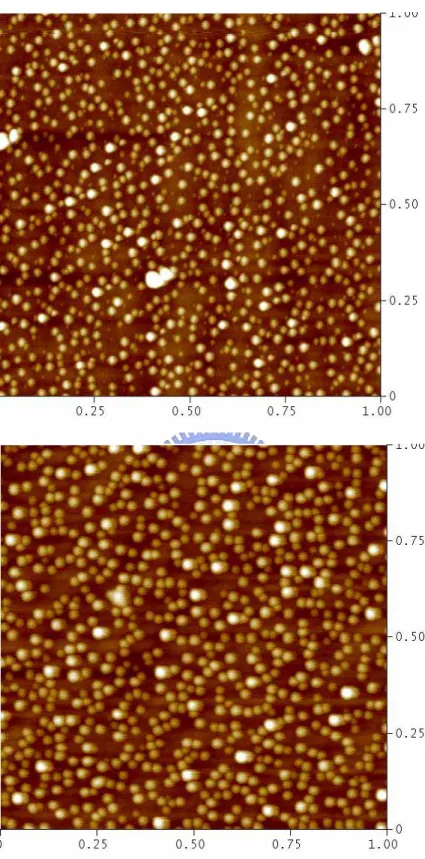
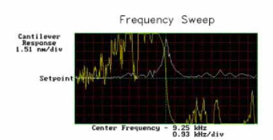
(29) Our system (as shown in Fig.2.5) is a Digital Instruments MultiMode SPM, which basically consists of the optical head and the base. The scanner is installed within the base, and the measured sample is mounted on the top of the scanner. The optical head consists of sample space, a laser diode, mirrors, and a four-quadrant positional photodetector. The tip on the cantilever is vibrated by bimorph at its resonance. As it approaching to sample surface, the tip-sample interaction causes a change in the amplitude, the phase, and the resonance frequency of the vibrating cantilever. Therefore, during operating in tapping mode, the feedback loop keeps the cantilever to vibrate at constant amplitude (constant-force mode) by extending or retracting the scanner as it is simultaneously raster-scans in X and Y directions. Finally, the “history” of scanner movement in Z across the sample surface is converted into a 3D image of the height data. Finally, it is necessary to note that we should check the tips used in the measurement carefully because the results of AFM images are strongly dependent on the shape and radius of the tip. Figure 2.6 shows that the surface morphology of QDs in the same sample with different tips. The measured result is approximately the sum of the nanostructures’ real size and the tip’s diameter. Therefore, a ‘very uniform’ size distribution of the nanostructures would be obtained and is nearly equal to the tip’s diameter when the tip’ size is much lager than nanostructures’.. • Brief description of operation principle The basic principle of operation in the tapping mode AFM can be simply and phenomenally described with a forced oscillation with damping. The equation of motion and its solution have the form. 16.
(30) ••. •. x + 2β x + ω o =. x. p. =. 2. F. F cos ωt m. cos(ωt − δ ). m. (ω − ω ) + 4β ω 2. 2 2. 2. 2. o. ⎛ 2 βω 2 2 ⎝ ωo − ω. δ = tan −1 ⎜⎜. ⎞ ⎟⎟ ⎠. where F, ω, ωo , and β are driving force, driving frequency, cantilever’s resonant frequency and damping constant respectively. The solution consists of homogeneous (which is omitted above) and particular parts. The homogeneous solution comprises an exponent term derived from the damping, and would decay rapidly. The particular term is a steady-state solution. From the formula above, the amplitude and phase of the oscillation changes with damping β. The relations between the amplitude (phase) and oscillation frequency of the cantilever are shown in Fig.2.7. Figure 2.8 gives the shift in amplitude (phase) at the fixed frequency due to the tip-sample interaction. There are at least three types of data recorded in the tapping mode AFM measurement: height, amplitude, and phase image. As mentioned above, the height image records the ‘traveling’ of scanner needed to keep the amplitude of the cantilever constant. On the other hand, the amplitude image is the change in amplitude of cantilever due to tip-sample interaction, and phase imaging is the mapping of the phase lag between the periodic signal that drives the cantilever and the oscillations of the cantilever.. 17.
(31) References [2.1] E. H. C. Parker, The technology and physics of molecular beam epitaxy, London, England (1985). [2.2] M. A. Herman and H. Sitter, Molecular beam epitaxy Fundamentals and current status, Springer (1996). [2.3] V. Swaminathan and A.T. Macrander, Materials aspects of GaAs and InP based structures, Prentice Hall, Inc. (1991) [2.4] S. N. Magonov and M.H. Whangbo, Surface analysis with STM and AFM (1996).. 18.
(32) Cryo-pump. Fig.2.1 A schematic of our Varian Gen II MBE system.. 19.
(33) Fig.2.2 One of measured RHEED oscillations in our system.. 20.
(34) In820 Growth Rate 1.8000E-07. y = 5.306746E-07x + 8.107959E-09 R2 = 9.983988E-01. 1.6000E-07 1.4000E-07. BF (torr). 1.2000E-07 1.0000E-07. In_820 GR 線性 (In_820 GR). 8.0000E-08 6.0000E-08 4.0000E-08 2.0000E-08 0.0000E+00 0. 0.05. 0.1. 0.15. 0.2. 0.25. 0.3. GR (um/hr). Fig.2.3 One of calibrated plots for growth rate and beam flux equivalent pressure.. 21.
(35) Argon Laser M1 Lock-in Amp.. PC. Chopper PD Sample. Si-PMT Monochromator (SPEX-1404). Cryo-Stat. M2 L2. L1. Fig.2.4 A schematic of the PL measurement system.. 22.
(36) Fig.2.5 MultiMode SPM (upper image) and optical head (lower image).. 23.
(37) Figure 2.6 AFM images of QDs in the same sample taken with different tips. 24.
(38) Fig. 2.7 The relations between the amplitude (phase) and oscillation frequency of the cantilever. Fig. 2.8 The amplitude (phase) shift at the fixed frequency due to the tip-sample interaction 25.
(39) Chapter 3 InAs/GaAs quantum dots growth and characterization. In this chapter, the studies of self-assemble InAs quantum dots (QDs) growth on (100) GaAs substrate are presented. The investigation of QDs growth and characterization were carried out, which were based on the previous results in our laboratory. First of all, the fabrication methods of QDs and the mechanism of the self-assembled growth (Stranski-Krastanow mode) are introduced. Then, the previous results of growth conditions dependence of the QDs are reviewed briefly. At last, the studies of growth parameters dependence of the QDs are demonstrated.. 3.1 Introduction to QDs fabrication. 3.1.1 Fabrication methods of QDs There has been a great amount of effort expended in the QD fabrication methods during the last two decades. The most conventional method is to lateral pattern the quantum well structure by electron beam lithography and wet or dry etching. However, lithography- and etching-based technologies will damage the structure and lead to defect problem. In order to overcome the surface state problem, two new techniques were introduced in early 1990s. In 1993, a novel fabrication technique, which was so-called. thermal. etching,. was. developed. to. construct. high-quality. and. surface-state-free QDs [3.1]. This technique utilizes the property of different thermal desorption rates between different materials to result in nonuniform thermal evaporation in a thin epilay to create QDs. Figure 3.1 illustrates the growth procedure. 26.
(40) of thermal etching. Besides, Stranski-Krastanow (S-K) growth mode is also a promising approach to produce QDs [3.2]. The pyramidal-shaped QDs are formed by S-K transition at the early stage of the strained growth and are a consequence of the elastic relaxation of the strain caused by the lattice mismatch between the epilay and the substrate. In the InAs/GaAs system, the lattice mismatch is about 7%. Figure 3.2 illustrates the typical growth procedure of InAs QDs on GaAs. The deposition of InAs on GaAs substrate maintains 2-D layer by layer growth in the first few monolayers (MLs). However, with the increasing strain energy induced by the lattice mismatch, the S-K transition takes place at certain deposition, so-called critical thickness. At the same time, the RHEED pattern transforms from a (2x4) streaky pattern to a spotty pattern, indicating the presence of 3D islands on the sample surface. From previous results, the typical critical thickness of InAs on GaAs system is about 1.4~1.7 MLs.. 3.1.2 Growth mechanism of self-assembled QDs: Stranski-Krastanow mode There are three modes of crystal growth on the surfaces, which was classified by Ernst Bauer in 1958 [3.3-3.6]. They are Frank-van der Merwe (F-M), Volmer-Weber (V-W), and Stranski-Krastanow (S-K) modes, as illustrated in Fig.3.3. In the epitaxy of hetero-structures, the growth modes are determined with the overall free energy, such as surface, volume and interface free energies. If we deposit the material “A” on substrate “S” under definite conditions, and the overall free energy of the system decreases faster over the first monolayer (or two), 2-D layer by layer growth mode will proceed, that is called F-M mode (left one in Fig.3.3). On the other hand, it favors the island or the V-W mode (middle one in Fig.3.3) as the overall energy increases faster over the first monolayer (or two). In an intermediate case, the layer-plus-island or S-K mode turns out (right one in Fig.3.3).. 27.
(41) In practice, the SK growth mode often applies to the strained layer heteroepitaxy, such as QDs growth. The accommodation of misfit strain between the epilayers and substrate changes the balance among the free energies because the strain energy increases with the film thickness. Therefore, a 2D layer growth may be favored initially, and the further deposition of material lead to the appearance of 3D islands within which strain is relaxed and their free energies decrease.. 3.1.3 Brief overview of previous results [3.7] There has been a great mount of effort in studies of growth condition dependence of InAs QDs in our laboratory. The results showed that substrate temperature, As beam flux, and InAs growth rate play important roles on InAs growth and have strong influence on transition energy levels [3.8-3.11]. Roughly speaking, higher substrate temperature, higher As beam flux, and lower InAs growth rate for QDs growth give a lower ground state transition energy due to larger indium diffusion length or less In-Ga intermixing. There still exist several parameters for QDs growth, such as GaAs capped growth rate, As2/As4 ratio, As beam flux, and so on. In this chapter, we will discuss the effects of these factors on InAs growth based on previous results.. 3.2 Self-assembled InAs/GaAs QDs growth by MBE. 3.2.1 MBE growth and sample structures A typical structure is designed for PL and AFM studies of InAs QDs, which is schematically shown in Fig. 3.4. The PL structure comprises a layer of InAs QDs, a pair of GaAs spacers, and a pair of Al0.3Ga0.7As carrier confinement layers. Besides, there is 28.
(42) an uncapped InAs QDs layer grown on top surface of the structure, which is used for AFM studies. The basic growth procedure and condition are given here. However, other special approaches will be described in the respective chapter. After native oxide desorpted under As flux at 610oC, a 2500Å GaAs buffer layer was deposited at 570oC to recover the substrate surface. 300 Å Al0.3Ga0.7As and 1400 Å GaAs were deposited at a growth rate of 1µm/hr at the same temperature. Then, 100 Å GaAs was grown at a growth rate of 0.3µm/hr. In the meanwhile, the substrate temperature is lowered down (510oC ~530oC) for InAs deposition, and the desired As flux for QDs growth was achieved by adjusting the needle valve of the As cracker cell. Afterwards, 10nm GaAs capped layer was deposited at the same temperature of QDs growth with a growth rate of 1µm/hr (or 0.3µm/hr.). Then the substrate temperature and As flux were raised to the original values for GaAs and Al0.3Ga0.7As growth. Finally, a layer of uncapped QDs was grown with the same conditions, and then the substrate cooled down under As flux immediately.. 3.2.2 Sample characterization After MBE growth, the samples were characterized by AFM and PL. One of the uncapped InAs QDs AFM images is shown in Fig.3.5. The sheet density of the QDs is about 3x1010cm-2, and the height is about 5nm, respectively. As mentioned in the previous chapter, the tip used for AFM measurement has strong influence on shape and size. Therefore, it is difficult to identify the real shape of QDs from AFM. Besides, it should be noted that the shape and size of QDs buried in the GaAs would change due to strong In-Ga intermixing induced by lattice mismatch between InAs and GaAs, [3.12]. We will study this in the next section and the following chapter. Figure 3.6 shows the results of the PL under different excitation powers at ~30 K.. 29.
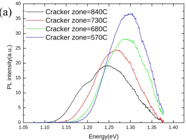
(43) We can observe the state filling effect in the figure. We also found that, from the curve with smallest excitation power (1mW) fitting by a multi-peak Gaussian function, the ground state energy, full-width-half-maximum (FWHM), and the energy level difference between ground and first excitation states are about 1.07eV, 29meV, and 65meV, respectively.. 3.3 Growth conditions of self-assembled InAs/GaAs QDs Several growth conditions are studied in this section. They are As2/As4 ratio, GaAs capped growth rate, and As beam flux. In order to study the effects on transition energy and uniformity of QDs for clarity, higher substrate temperatures (510~530oC), and lower InAs growth rates (0.056µm/hr and 0.0373µm/hr) are used in the experiments. Detailed growth conditions are listed in Table 3.1.. 3.3.1 As2/As4 ratio [3.13] It is well known that the influence of arsenic species (As2 and As4) on MBE growth is quite different. Especially for InAs QDs growth, the effect of As beam flux is very different with that for 2-D growth. In practice, the sticking coefficient of As4 has been shown to be half that of As2. To investigate this effect on QDs growth, various As2/As4 mixtures are used. We can obtain a desired mixture of As2/As4 vapor by altering the cracker zone temperature of the As valved cracker cell. The cracker zone temperatures used in the experiments are 840oC, 730oC, 680oC, and 570oC. For As2 (As4) mode, the temperature of the cracking zone is kept at about 840oC (570oC). On the other hand, the As cracker cell provides a mixture of As2/As4 as the temperature is set at 730oC (680oC). The AFM images of QDs shown in Fig. 3.7 and Fig. 3.8 demonstrate a significant feature in the surface morphology: There is a tendency that 30.
(44) the density and the size uniformity of QDs are improving with increasing the percentage of As4 in the mixture. This result could be explained in the following way: The QDs form in the early stage (or so-called “seed”) can collect InAs from their neighborhood and then grow gradually. The indium adatoms are more mobile and has a larger diffusion length in As2 atmosphere. Hence, the QDs using As2 flux can gather much more InAs from farther area. Lager QDs’ size and lower sheet density are achieved. In addition, it also exhibits a large fluctuation in QD size. In contrast, The QDs using As4 flux can only collect InAs from a fixed region of their vicinity. This leads to a smaller size dimension and a higher sheet density of QDs. Furthermore; the size uniformity is also improving due to collecting a fixed amount of InAs under As4 beam flux. The AFM images show these facts no matter what As BEP is (on condition that no growth interruption after InAs deposition). From the PL results in Fig.3.9, it shows little dissimilarity among various As2/As4, if V/III ratio is lower during InAs deposition. The reason is that, for QD growth under low As BEP, the In adatoms migrate on the grown surface easily and then find their proper sites both in As2 and As4 atmosphere. On the contrary, there is an obvious difference, if V/III ratio remains high. The In adatoms tend to stop at improper sites under high As BEP, resulting in a broad distribution. Especially, it shows a multi-fold distribution if the percentage of As2 is increasing in the mixture. The reason is the same as above.. 3.3.2 GaAs capped growth rate In order to obtain high optical activity, the QDs need to be protected via the growth of the capping GaAs layer. As mentioned above, the inter-diffusion or intermixing would take place as the overgrowth of GaAs on InAs QDs due to a large misfit strain. 31.
(45) between them. Therefore, the condition of GaAs overgrowth plays an important role in transition energy level of QDs, such as As beam flux and capped growth rate. Previous studies gave a conclusion that a higher As beam flux would reduce the diffusion length of InAs and GaAs on the surface and then depress the inter-diffusion (or intermixing) between GaAs and InAs. In this subsection, the effect of capped growth rates (0.3µm/hr or 1µm/hr) is studied. Figure 3.10 shows that there is no or little difference between higher and lower capped growth rate when substrate temperature is 520oC. The reason is given as follows: Alloying is a strong temperature-dependent process. The rapid In(Ga)As alloying effect occurs around the periphery of the QDs during GaAs overgrowth even though the capped rate is low. The formed alloy inhibits successive Ga adatoms to diffuse inward and intermix with InAs further. For that reason, the capped growth rate has no or little effect on InAs QD growth, as compared to As BEP. However, as GaAs being capped at low temperature, the growth rate would influence the growth of QDs. We will show this in the chapter 6. 3.3.3 As beam flux The diffusion length of adatoms on the surface is strongly dependent on the growth conditions, such as molecular species (In, Ga, or Al / As2 or As4), substrate temperature, arsenic BEP. Adatoms’ diffusion length and intermixing usually determine QDs’ size distribution and their transition energy. As warming up the As valved cracker cell for growth, the arsenic bulk material needs at least two hours to reach thermal equilibrium due to its large thermal mass. However, in practice, the arsenic BEP will increase gradually with time. In other words, the vacuum pressure of growth chamber is rising steadily. By exploiting this feature and without adjusting the As needle valve during epitaxial deposition, we can perform. 32.
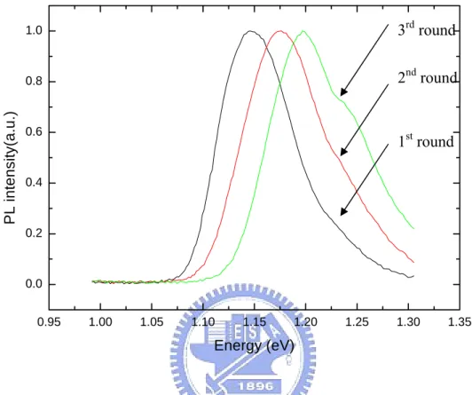
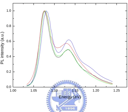
(46) successively three identical experiments to monitor the growth of QDs. The growth condition is given as follows: 2.6 MLs of InAs is deposited at 520oC with a growth rate of ~0.056µm/hr. In Fig.3.11, there are twofold size distributions of PL in all samples. There always exists a peak value of PL spectrum, whose transition energy is ~1.235eV (see the arrows), under this growth condition. We attribute this to the emission from the QDs that formed immediately after S-K transition. The other peak values are ranged from 1.14~1.20eV. In the first round of the experiment, most of the QDs grew gradually by absorbing In from their vicinity. However, with increase of As BEP, it would be to suppress the migration of In adatom and result in a group of QDs that is smaller than that of the first round. This result manifests the growth and decline of QDs in the S-K mode.. 3.3.4 Remark In order to solve the problem of slow response of arsenic BEP due to large thermal mass of the bulk material and obtain repeatable results in the different growth rounds, an annealed process was used. After QDs growth, the QDs are next annealing for a few seconds (30~60s), so that indium adatoms have enough time to migrate to appreciate sites on the surface to enhance the size distribution (shown in Fig.3.12). Besides, by altering the growth parameters of InAs QDs, the maximum of PL peak wavelength just extend to near 1.25µm at room temperature, no matter what substrate temperature is used (510oC ~530oC). We attribute this to stronger In-Ga intermixing occurring in the larger QDs during GaAs overgrowth [3.12, 3.14-3.16]. Hence, how to suppress or inhibit intermixing, or strain redistribution, during overgrowth is the main factor that extending the emission wavelength.. 33.
(47) 3.4 Summary In summary, the growth and characterization of InAs QDs have been investigated extensively. The results of AFM and PL of grown QDs are used to study the growth condition dependence. The growth parameters, such as GaAs capped growth rate, As2/As4 ratio, and arsenic beam flux, have been studied and discussed extensively. We found that the diffusion of group III atoms is dominating factor in the QDs growth. Arsenic molecular species would influence group III adatoms’ migration behavior on the surface. Besides, the capped growth rate has no or little effect on the QDs growth if the alloying effect dominates. We also study the growth and decline of QDs after S-K transition by a sequence of identical experiments.. 34.
(48) References. [3.1] D. C. Liu and C.P. Lee, Appl. Phys. Lett. 63, 3503(1993) [3.2] L. Goldstein, F. Glas, J. Y. Marzin, M. N. Charasse and G. Le Roux, Appl. Phys. Lett. 47, 1099 (1985). [3.3] J. Y. Tsao, Materals fundamentals of molecular beam epitaxy, Academic press, Inc. (1993) [3.4]. W.K. Liu and M.B. Santos, Thin films: heteroepitaxial systems, World Scientific, (1999) [3.5] Mitsuru Sugawara, Self-assembled InGaAs/GaAs quantum dots, Academic press, Tokyo, Japan (1999). [3.6].W. Seifert, N. Carlsson, M. Miller, M. Pistol, L. Samuelson, and L. R. Wallenberg, Prog. Crystal Growth and Charact. 33, 423 (1996) [3.7].S. D Lin, Doctoral dissertation, NCTU, Tawain(2002) [3.8] G. S. Solomon, J. A. Trezza, and J. S. Harris, Jr., Appl. Phys. Lett. 66, 991 (1995). [3.9] G. S. Solomon, J. A. Trezza, and J. S. Harris, Jr., Appl. Phys. Lett. 66, 3161 (1995). [3.10] L. Chu, A. Arzberger, G. Böhm and G. Abstreiter, J. Appl. Phys. 85, 2355 (1999). [3.11] M. G. Alessi, M. Capizzi, A. S. Bhatti, A. Frova, F. Martelli, P. Frigeri, A. Bosacchi, and S. Franchi, Phys. Rev. B 59, 7620 (1999). [3.12]J. M. Garcia, G. Medeiros-Ribeiro, K. Schmidt, T. Ngo, J. L. Feng, A. Lorke, J. Kotthaus, and P. M. Petroff, Appl. Phys. Lett. 71, 2014 (1997). [3.13] E. H. C. Parker, The technology and physics of molecular beam epitaxy, London, England (1985). [3.14] J. M. Garcia, J. P. Silveira, and F. Briones, Appl. Phys. Lett. 77, 409 (1997) [3.15]Ferdos, Fariba; Wang, Shumin; Wei, Yongqiang; Sadeghi, Mahdad; Zhao, Qingxiang; Larsson, Anders, J. Crystal. Growth, 251,145(2003). 35.
(49) [3.16] Heyn, Ch.and Hansen, W, J. Crystal. Growth, 251,140(2003). 36.
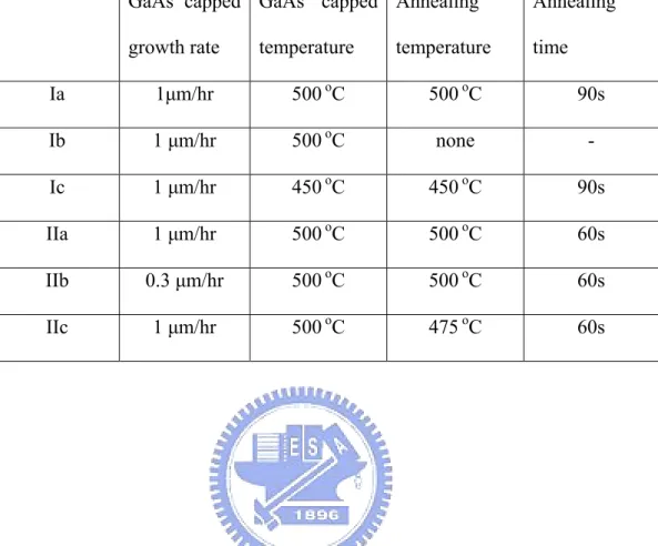
(50) Table 3.1 InAs QDs growth parameters. Lm3835(2.5ML) Lm3836(2.5ML) Lm3837(2.5ML) Lm3838(2.5ML) Lm3885(2.5ML) Lm3886(2.5ML) Lm3887(2.5ML) Lm3888(2.5ML) Lm3911(2.5ML) Lm3912(2.5ML) Lm3913(2.5ML) Lm3914(2.5ML). As cracker temperature. GaAs capping layer growth rate. 840 ℃ 730 ℃ 680 ℃ 570 ℃ 840 ℃ 730 ℃ 680 ℃ 570 ℃ 570 ℃ 680 ℃ 730 ℃ 840 ℃. 0.3 μm/hr 0.3 μm/hr 0.3 μm/hr 0.3 μm/hr 1.0 μm/hr 1.0 μm/hr 1.0 μm/hr 1.0 μm/hr 1.0 μm/hr 1.0 μm/hr 1.0 μm/hr 1.0 μm/hr. 37. As beam flux As beam flux during InAs during other deposition (torr) deposition (torr) ~5.3e-6 ~5.3e-6 ~7.9e-6 ~7.9e-6 ~9.4e-6 ~9.4e-6 ~1.24e-6 ~1.24e-6 ~3.8e-6 ~3.8e-6 ~5.4e-6 ~5.4e-6 ~5.9e-6 ~5.9e-6 ~7.8e-5 ~7.8e-5 ~1.23e-5 ~7.1e-6 ~9.5e-6 ~5.6e-6 ~7.6e-6 ~4.9e-6 ~5e-6 ~3e-6.
(51) Fig.3.1 Fabrication procedure of ‘thermal etching’ quantum dots. 38.
(52) Start from (100) GaAs substrate. GaAs buffer layer growth. InAs 2-D layer deposition. InAs 3-D island formation. GaAs capping layer deposition. Fig.3.2 Growth procedure for InAs/GaAs QDs in S-K mode.. 39.
(53) A B. FM. VW. SK. Fig.3.3 Three growth modes in heterostructure epitaxy, Frank-van der Merwe (F-M), Volmer-Weber (VW), and Stranski-Krastanow (S-K).. 40.
(54) InAs QDs 20nm GaAs 30nm Al0.3Ga0.7As 150nm GaAs InAs QDs 150nm GaAs 30nm Al0.3Ga0.7As ~250nm buffer GaAs (100) GaAs substrate Fig.3.4 A typical sample structure of InAs QDs growth, the top InAs QDs are used in AFM measurement.. 41.
(55) Fig.3.5 AFM images of uncapped InAs QDs.. 42.
(56) 25. 200uW 1mW 5mW 14mW. PL intensity(a.u.). 20. 15. 10. 5. 0 1.00. 1.05. 1.10. 1.15. 1.20. 1.25. Energy(eV). Fig.3.6 The PL spectrum of grown InAs/GaAs QDs measured under different excitation powers. 43.
(57) Cracker zone=840℃. Cracker zone=730℃. Cracker zone=680℃. Cracker zone=570℃. Fig.3.7 The surface morphology of uncapped InAs QDs using a mixture of As2/As4 vapor (on condition that a high V/III ratio is used during InAs deposition). 44.
(58) Cracker zone=840℃. Cracker zone=730℃. Cracker zone=680℃. Cracker zone=570℃. Fig.3.8 The surface morphology of uncapped InAs QDs using a mixture of As2/As4 vapor (on condition that a low V/III ratio is used during InAs deposition). 45.
(59) (a). 40 35. PL intensity(a.u.). 30. Cracker zone=840C Cracker zone=730C Cracker zone=680C Cracker zone=570C. 25 20 15 10 5 0 1.05. 1.10. 1.15. 1.20. 1.25. 1.30. 1.35. 1.40. 1.30. 1.35. 1.40. Energy(eV). (b). 20 18 16. PL intensity(a.u.). 14. Cracker zone=570C Cracker zone=680C Cracker zone=730C Cracker zone=840C. 12 10 8 6 4 2 0 1.05. 1.10. 1.15. 1.20. 1.25. Energy(eV). Fig.3.9. The PL spectrum of grown InAs QDs using a mixture of As2/As4 vapor (a) with a high V/III ratio , (b) with a low V/III ratio during InAs deposition. 46.
(60) (a). 40 35. PL intensity(a.u.). 30. Cracker zone=840C Cracker zone=730C Cracker zone=680C Cracker zone=570C. 25 20 15 10 5 0 1.05. 1.10. 1.15. 1.20. 1.25. 1.30. 1.35. 1.40. 1.30. 1.35. 1.40. Energy(eV). (b) 50 45 40. PL intensity(a.u.). 35. Cracker zone=840C Cracker zone=730C Cracker zone=680C Cracker zone=570C. 30 25 20 15 10 5 0 1.05. 1.10. 1.15. 1.20. 1.25. Energy(eV). Fig. 3.10 The PL spectrum of grown InAs QDs under different capped growth rate (using a mixture of As2/As4 vapor). (a) 1µm/hr, (b)0.3µm/hr. 47.
(61) PL intensity(a.u.). 1.0. 3rd round. 0.8. 2nd round. 0.6. 1st round. 0.4. 0.2. 0.0 0.95. 1.00. 1.05. 1.10. 1.15. 1.20. 1.25. 1.30. 1.35. Energy (eV). Fig. 3.11 The PL spectrum of grown InAs QDs (without growth interruption). 48.
(62) 1.0. PL intensity (a.u.). 0.8. 0.6. 0.4. 0.2. 0.0 1.00. 1.05. 1.10. 1.15. 1.20. 1.25. Energy (eV). Fig. 3.12 The PL spectrum of grown InAs QDs (with growth interruption). 49.
(63) Part A. Ordered Quantum Dots Lattice Growth. 50.
(64) Chapter 4 Selective growth of InAs quantum dots array on patterned GaAs(001) substrates. In this chapter, we study the MBE selective growth of InAs QDs on GaAs(100) substrates patterned by e-beam lithography and wet chemical etching. The purpose of QDs selective growth and a brief review are given. Then, the experiments about substrate patterning and MBE growth are presented. Various samples characterization and discussion are summarized finally.. 4.1 Introduction. 4.1.1Purpose to use selective growth on self-assembled QDs InAs self-assembled QDs grown by S-K mode have been intensively studied in the last several years due to their fabrication-easy and defect-free properties. The high crystalline quality found in QDs formed by these processes enables incorporation of the dots in optical and electronic devices. However, the stochastic nature of the formation of these QDs driving by the elastic relaxation of the strain leads to undesirable nonuniformity in their sizes as well as their spatial distribution. The size fluctuation results in large inhomogeneous broadening in their energy spectrum. Besides, it is almost impossible to place the QDs in a long-range-ordering manner or on the designated locations. These seriously limit the potential device applications of such QDs. As for size fluctuation, recent studies concentrated on the formation of high. 51.
(65) density and uniform sized QDs by optimizing the growth conditions. On the other hand, there has been increasing interest in the study of self-assembled QD selective formation on the grown surfaces, designed to improve position control.. 4.1.2 Overview of selective growth methods The common selective growth methods of self-assembled QDs can be classified into two categories: (a) patterned substrate methods and (b) strain engineering methods.. • Patterned substrate methods [4.1-4.9] The method is based on the differences in migration behaviors or sticking coefficient of group III adatoms on the faceted surface: D. S. L. Mui et al. made use of differences in atom diffusion on faceted surfaces to control QDs formation. M. Kitamura et al. grew QDs on the step edges of multi-atomic steps that result from the step bunching. R. Zhang et al. utilized selective area epitaxy and oxide-patterned substrate to position QDs on GaAs facet. C.Y. Hyon et al. selectively positioned QDs on GaAs patterning by AFM nanolithography. T. Fukui et al. demonstrated positionand number-controlled QDs via selective area epitaxy and SiNx (or SiO2)-patterned substrate. B.H. Choi et al. demonstrated almost one-dimensional alignment of QDs on Si substrate. S.C. Lee et al. fabricated a one-dimensional row of QDs using Orientation-dependent migration and incorporation of In atoms from (111)A to (100) facets. X. Mei et al. utilized anodic Al2O3 nanohole array template mask to fabricate QDs array.. • Strain engineering methods [4.10-4.13] This technique makes use of introducing a build-in or artificial strain anisotropy. 52.
(66) on the grown surface to control QDs formation: H. Lee et al. combined lithography with in situ lateral strain engineering to control QDs formed on mesoscopic surface. T. Mano et al. demonstrated a one-dimensional alignment of QDs by lateral surface strain field modulation generated by the underlying InGaAs superlattice template. 4.2 Experiments. 4.2.1 Electron-beam patterning Two chessboard-like patterns with sizes of ~ 80µm × 80 µm were first defined on a flat (001) GaAs substrate via e-beam nanolithography and the wet chemical etching. Figure 4.1(a) shows a schematic diagram of the grid pattern defined on the GaAs substrate. The two chessboard-like patterns were composed of cross stripes oriented at angles of 0◦, 90◦ (pattern A) and 45◦, 135◦ (pattern B) with respect to the [110] direction. On both pattern A and pattern B, those have a pitch size of 0.1 µm. The GaAs substrate was first covered with 2% PMMA, and then exposed to an e-beam to define the patterns. After PMMA development and wet chemical etching in a H2SO4:H2O2:H2O=1:8:80 solution, the e-beam-defined patterns were transferred onto the GaAs substrate. Figure 4.1(b) shows the scanning electron microscope (SEM) images of the patterns after the wet chemical etching. The anisotropic etching rate for different faceted surface results in pits with area of about 150 nm ×100 nm and depth about 15 nm [4.14]. The pits on pattern A have their edges parallel to [110], [1-10]. For pits on pattern B, their edges are parallel to [100], [010]. The pits were rectangular in shape since the etching processes were anisotropic on the two perpendicular facets inside the pits. This resulted in different thicknesses of the walls surrounding the pits. For example, on pattern A, the walls parallel to [110] are thinner than the walls along [1-10]. 53.
(67) 4.2.2 MBE regrowth Before introducing the patterned substrate into the MBE system, the wafer was cleaned in solvents and a thin layer of GaAs was removed from the top using wet chemical etching using H3PO4:H2O2:H2O = 3:1:50. The purpose of this procedure is to remove the contaminations that introduced from PMMA development and successive process. The MBE growth process started with oxide desorption under an As2 flux at 610oC.After the oxide layer was removed, a 100Å GaAs buffer layer was deposited at 610oC to recover the etched surface. Then the substrate temperature was lowered to 520oC to deposit 2MLs of InAs at a growth rate of about 0.056µm/hr. Finally, 500Å GaAs capped layer was grown at the same temperature and then cooled down under As2 flux. In order to investigate the effect of patterned substrate on QDs growth, we deposited 2ML of InAs, which is above the critical thickness of S-K transition. The QDs were formed on both patterned (A and B) and non-patterned regions, under the same growth conditions. The same procedure was repeated for AFM sample, except that after the QDs growth, the growth was stopped and then cooled down under As2 flux immediately.. 4.3 Results and discussion. 4.3.1 TEM and AFM characterization The transmission electron microscope (TEM) image of the QDs formed on the non-patterned area is shown in the upper part of Fig.4.2. We have also shown the AFM images taken from the centre of pattern A in Fig.4.3. The AFM image in Fig.4.3 looks slightly different from the SEM image of the e-beam defined pattern shown in Fig.4.1. 54.
(68) The reason is that the wet chemical etching process operative before introducing the patterned sample into the MBE chamber has effected further thinning of the stripes parallel to [110] on pattern A. Therefore, the image of the stripes parallel to [110] is not evident in Fig.4.3. Nevertheless, the inset in Fig.4.3 shows that only a single row of dots was formed on stripes parallel to [1-10]. Those stripes have top widths of about 50 nm. The dots that appeared on the stripes have an average base width of about 30 nm and are more uniform in size than dots formed on the non-patterned area. It is worth to note that no dot was found on a stripe parallel to [110] due to its much narrower top width. The AFM image taken from the inside of the pits on pattern A is also given in Fig.4.4. The inset in Fig.4.4 indicates that there is also a single row of dots formed inside the pits. The position of those dots that appeared inside the pits looks asymmetric with respect to the centre of the pits. The TEM image of QDs on pattern A as shown in Fig.4.5 is also consistent with results from the AFM images. In contrast to the results on pattern A, the TEM image of the dots on pattern B (as shown in Fig.4.6) shows that the dots were only grown inside the pits and no dots can be found on the top of mesas. This is due to the undercut edges of the etched sidewalls of the pits, which have prevented the dots from being grown on the top of the stripes. The estimated density of the QDs formed on pattern A is about 3 × 1010 cm−2 and is much higher than the densities of those on pattern B (about 4 × 109 cm−2) and the non-patterned area (about the same as for pattern B).. 4.3.2 Photoluminescence studies We have studied and compared the PL spectra from the QDs grown on pattern A, pattern B and the non-patterned area after the samples were capped with 50 nm GaAs. In Fig.4.7, we have shown the PL spectra of the QD sample taken from three different 55.
(69) region of the sample: pattern A, the non-patterned area and pattern B. The QDs grown on pattern A emitted the strongest PL intensity among the three (about four times stronger than that from the other areas). We attribute this to the improvement of the dot quality and the higher density of QDs formed in this area. It also indicated that our patterned surface has recovered during the regrowth from the processing damage. The peak of the luminescence also showed a significant blue shifting (about 25 meV) compared to the luminescence signal from the dots on the non-patterned area. This indicates that quantum dots formed on pattern A are different in size and composition compared to the dots on pattern B and on the non-patterned area. For QDs grown on pattern B, the luminescence intensity and peak position are not very different from those for dots on the non-patterned area.. 4.4 Summary In summary, we have grown QDs via molecular beam epitaxy on patterned GaAs(001) substrates prepared by e-beam lithography and wet chemical etching. TEM and AFM images show ordering of QDs formed on the stripes and inside the pits. From PL studies, we found that the QDs grown on pattern A gave the strongest luminescence intensity among the three areas that we have investigated. We attribute this to the higher density, ordering and improvement in quality of the dots. .. 56.
(70) References. [4.1] D. S. L. Mui, D. Leonard, L.A. Coldren, and P. M. Petroff, Appl. Phys. Lett. 66, 1620 (1995). [4.2] M. Kitamura, M. Nishioka, J. Oshinowo, and Y. Arakawa, Appl. Phys. Lett. 66, 3663 (1995). [4.3] R. Zhang, R. Tsui, K. Shiralagi, D. Convey, and H. Goronkin, Appl. Phys. Lett. 73, 505 (1998). [4.4] C. K. Hyon, S. C. Choi, S.-H. Song S. W. Hwang, M. H. Son, D. Ahn, Y. J. Park and E. K. Kim, Appl. Phys. Lett. 77, 2607 (2000). [4.5] Cheol-Koo Hahn, Junichi Motohisa, and Takashi Fukui, Appl. Phys. Lett. 76, 3947 (2000). [4.6] Hyo Jin Kim, Junichi Motohisa, and Takashi Fukui Appl. Phys. Lett. 81, 5147 (2002). [4.7] B. H. Choi, C. M. Park, S.-H. Song, M. H. Son, S. W. Hwang, D. Ahn, and E. K. Kim, Appl. Phys. Lett,78, 1403 (2001). [4.8] S. C. Lee, L. R. Dawson, K. J. Malloy, and S. R. J. Brueck, Appl. Phys. Lett. 79, 2630 (2001). [4.9] X. Mei, D. Kim, H. E. Ruda,and Q. X. Guo, Appl. Phys. Lett. 81, 361 (2002). [4.10] H. Lee, J. A. Johnson, M. Y. He, J. S. Speck, and P. M. Petroff, Appl. Phys. Lett. 78, 105 (2001). [4.11] T. Mano, R. No¨ tzel, G. J. Hamhuis, T. J. Eijkemans, and J. H. Wolter, Appl. Phys. Lett, 81, 1705 (2002). [4.12] Kwang Moo Kim, Young Ju Park, Young Min Park, Chan Kyeong Hyon, Eun. 57.
(71) Kyu Kim, and Jung Ho Park, J. Appl. Phys. 92, 5453 (2002). [4.13] T. Mano, R. No¨ tzel, G. J. Hamhuis, T. J. Eijkemans, and J. H. Wolter, J. Appl. Phys. 95, 109 (2004). [4.14] R. E. Williams, Gallium arsenide processing techniques (1984). 58.
(72) [1-1 0]. [1 1 0]. Pattern A. Pattern B. Fig.4.1 (a) Two types of square grids patterns with pitch of 0.1µm, (b) SEM images of the patterns after the wet chemical etching. 59.
(73) Fig.4.2 The TEM image of the uncapped QDs on the non-patterned area (in the upper half of the figure) and pattern B (in the lower half part).. 60.
(74) Fig.4.3 The AFM images of QDs grown on the pattern A. The inset shows a single row of dots that formed on the mesa stripes. 61.
(75) Fig.4.4 The AFM images of QDs inside the pits of pattern A. The inset also shows one single row of dots sited against one of the sidewalls.. 62.
(76) Fig.4.5. The TEM image shows that dots formed on the ridge and valley, which is consistent with the AFM image. 63.
(77) Fig.4.6 The TEM image shows that dots formed inside the pits only and no dot landed on the mesa top. 64.
(78) Fig.4.7 The PL spectra of the QDs sample are taken from three different areas: pattern A, non-patterned area, and pattern B.. 65.
(79) Chapter 5 Selective growth of single InAs quantum dots. In this chapter, a method to achieve long-range ordering and selective positioning of single InAs self-assembled QDs has been developed. The selective growth was achieved by manipulating the strain distribution on the sample surface. We have demonstrated single QD formation on small e-beam defined mesas. Controlled single dot arrays have also been achieved by using this technique.. 5.1 Introduction. 5.1.1 Single QDs fabrication The self-assembled quantum dots (QDs) grown by S-K mode are promising candidates for quantum devices because of ease of fabrication, and their high-quality, defect-free properties. However, as mentioned in the previous chapter, the ensemble of QDs grown using the S-K growth mode are usually randomly distributed on the grown surface and suffer from strain fluctuations in a random manner. It is almost impossible to place the QDs in a long-range ordered way or on the predesigned locations. These seriously limit the potential device applications of such QDs. Especially for single QDs; they should find applications in many new generation quantum devices, such as single electron transistors, single photon source, and single-photon photodetectors Recently, in order to solve these problems, there have been a great amount of efforts in the study of self-assembled QDs formation on patterned substrates to improve size uniformity and position controllability. However, as for single QDs fabrication,. 66.
數據
+4
相關文件
7 we define the critical exponents characterizing the singular behaviour of the parti- tion function and the susceptibilities of the order parameters as
O.K., let’s study chiral phase transition. Quark
We compare the results of analytical and numerical studies of lattice 2D quantum gravity, where the internal quantum metric is described by random (dynamical)
* Anomaly is intrinsically QUANTUM effect Chiral anomaly is a fundamental aspect of QFT with chiral fermions.
Monopolies in synchronous distributed systems (Peleg 1998; Peleg
In this study, we compute the band structures for three types of photonic structures. The first one is a modified simple cubic lattice consisting of dielectric spheres on the
Corollary 13.3. For, if C is simple and lies in D, the function f is analytic at each point interior to and on C; so we apply the Cauchy-Goursat theorem directly. On the other hand,
Corollary 13.3. For, if C is simple and lies in D, the function f is analytic at each point interior to and on C; so we apply the Cauchy-Goursat theorem directly. On the other hand,
