國 立 交 通 大 學
奈 米 科 技 研 究 所
碩 士 論 文
鉑矽化物奈米線生物感測器之製造與應用研究
Fabrication of Platinum-Silicide Nanowires for
Bio-electrical Sensor
研 究 生: 葉人豪 Jen-Hao Yeh
學 號: 9252507
指導教授: 劉增豐 博士 Dr. Tzeng-Feng Liu
柯富祥 博士 Dr. Fu-Hsiang Ko
中華民國九十四年六月
鉑矽化物奈米線生物感測器之製造與應用研究
Fabrication of Platinum-Silicide Nanowires for Bio-electrical
Sensor
研 究 生: 葉人豪 Student : Jen- Hao Yeh
指導教授: 劉增豐 博士 Advisor : Dr. Tzeng-Feng Liu
柯富祥 博士 Dr. Fu-Hsiang Ko
國 立 交 通 大 學
奈 米 科 技 研 究 所
碩 士 論 文
A Thesis
Submitted to Institute of Nanotechnology
College of Engineering
National Chiao Tung University
in partial Fulfillment of the Requirements
for the Degree of
Master
in
Institute of Nanotechnology
June 2005
Hsinchu, Taiwan, Republic of China
Acknowledgments
During my days as a graduate student in the Institute of Nanotechnology, National Chiao Tung University, many people have contributed their wisdom and advice to me. I thank them all for helping me to produce this Thesis.
I am particularly grateful to my advisors, Dr. Tzeng-Feng Liu and Dr. Fu-Hsiang Ko, who have always patiently guided and encouraged me. I have benefited a lot from their vision and advice, not only with respect to my studies but also with life’s experiences. My appreciation is also extended to the members of my oral defense committee for all of their valuable suggestions.
The help I have received from, and the discussions I have had with, my colleagues are too numerous to list in detail, but I am acknowledge my partner, Chieh-Tso Chen, and my older schoolmate, Chun-Chi Chen, who have given me a great deal of assistance and many suggestions for my experiments. In addition, I also am grateful to my classmates and younger schoolmates in the Institute of Nanotechnology, including Nicholas, Tzu-Yao, Tsu-Te, Jia-Hui, Wen-Hong, Tian-You, Su-Chen, Jian-Wen, Zhi-Wei, Kun-Lin, Yi-Jie, Jia-Dian, and Loris. I cherish the time that we shared together. I also thank the members of National Nano Device Laboratories for their support with the instrumentation facilities and experimental procedures.
Finally, to my family, my most devoted supporters: Thanks for your patience and understanding.
鉑矽化物奈米線生物感測器之製造與應用研究
研究生:葉人豪 指導教授:劉增豐 博士 柯富祥 博士國立交通大學奈米科技研究所 碩士班
摘 要
近年來一維奈米結構材料廣泛的被研究利用來當作高靈敏度的分子感測器, 能夠偵測的多種微小物質,例如:離子、蛋白質、DNA 以及氣體分子等等。在實驗 室裡,雖然奈米碳管或者矽奈米線可能達到單分子偵測的能力,但是其製作卻難 以與現代的半導體製程相容。為了改善這個缺點,在本論文中利用標準的半導體 製程技術,製造出經濟又大量的鉑矽化物奈米線感測元件。 首先,我們利用電子束微影技術(Electron-Beam Lithography)以及濕式蝕刻的 方法,製作出50-60nm 的多晶矽奈米線。在多晶矽奈米線表面沉積金屬鉑之後, 進行 400℃、450℃、500℃、550℃及 600℃快速退火,利用王水在 75℃的溫度下 將未參與反應的鉑蝕刻掉,能夠得到 40nm 的鉑矽化物奈米線。再者,我們在鉑矽 化物奈米線表面修飾上 APTMS,當作奈米線與 DNA 之間的 Linker,讓我們能夠將 單股 DNA 固定在奈米線表面,並偵測另一股特定序列的單股 DNA。利用鉑矽化物奈 米線表面電荷的不同會影響奈米線本身導電性的結果,來偵測特定序列的 DNA。並 且在實驗過程中利用 DNA 的螢光標定結果顯示,證明鉑矽化物奈米線確實是一良 好的 DNA 感測元件。Fabrication of Platinum Silicide Nanowires for Bio-electrical
Sensor
Student : Jen-Hao Yeh Advisor : Dr. Tzeng-Feng Liu Dr. Fu-Hsiang Ko
Institute of Nanotechnology
National Chiao Tung University
Abstract
One-dimensional nanostructures are good candidates for use in many applications as ultrasensitive, miniaturized molecule sensors for monitoring, for example, ions, proteins, DNA, and gases. Carbon nanotubes and silicon nanowires can behave as single-molecule biosensors, but the fabrication methods that been used to create such devices are not compatible with modern semiconductor manufacturing techniques, and large-scale integration is problematic. In this Thesis, we demonstrate the detection of DNA molecules, based on their intrinsic charge, by using a cheap polysilicon nanowire fabricated through standard “top-down” semiconductor processes.
First, we fabricated the 80-nm polysilicon nanowire through direct e-beam writing and shrank the width of the nanowire to 50–60 nm through wet etching. After depositing a thin platinum film using a sputtering system, we used rapid isothermal annealing technology to form the platinum silicide at temperatures ranging from 400 to 600 °C. The resulting wafers were immersed in a solution of HNO3/HCl/H2O (1:3:4) at
75 °C to remove any unreacted platinum. After this step, we obtained platinum silicide grain nanowires having final line widths that had shrunk to 40 nm; we determined the temperature at which they were most sensitive toward the intrinsic charge of DNA.
Next, we modified the nanowires’ surfaces for the goal of using them for biosensing. The platinum silicide surface was modified using APTMS to present amino groups and then single-stranded DNA was immobilized through these groups to allow the detection of its complementary single-stranded gene sequence. In a control experiment, we prepared a fluorescently labeled single-strand DNA so that we could observe, using fluorescence microscopy, that it did reside on the platinum silicide nanowire. Finally, we used a semiconductor analyzer to measure the conductance of the nanowires at each step of the modification process.
We fabricated this nanowire-based DNA device through a successful combination of top-down and bottom-up processes; this approach highlights the possibilities of fabricating sensor arrays at high density and directly integrating them into silicon-based circuitry.
Contents
Acknowledgment---Ⅰ
Chinese Abstract---Ⅱ
Abstract---Ⅲ
Contents---Ⅴ
List of Tables---Ⅶ
List of Figures---Ⅷ
Chapter 1: Introduction...1
1.1 General Introduction...1
1.2 Top-Down Nanotechnology...2
1.3 Bottom-Up Nanotechnology...7
1.4 Motivation ...11
1.5 Organization of Thesis...14
Chapter 2: Review and Design Concepts...15
2.1 Silicon Nanowire (Bottom-Up)...15
2.2 Silicon Nanowire (Top-Down)...19
2.3 Experimental Features...22
2.4 Detection Concepts...23
2.5 Electron Beam Lithography...24
3.1 General Information...26
3.2 Experimental Steps...28
3.2.1 Fabrication of a Polycrystalline Silicon Nanowire...28
3.2.2 Deposition of a Platinum Film and the Formation of the Platinum
Silicide...29
3.2.3 Self-Assembly of a Linker Layer Between the DNA and the
Nanowire...32
3.2.4 Detection of Complementary and Non-complementary
ssDNA...34
Chapter 4: Results and Discussion...37
4.1 Electrical Properties of the Polysilicon Nanowire...38
4.2 Electrical Properties of the Platinum Silicide Nanowire...39
4.3 Sensing of Multi-Steps-APTMS Modification, DNA Hybridization and
Denaturation...51
Chapter 5: Conclusions...57
Chapter 6: Future Work...58
List of Tables
Table 1.1...3
Overall roadmap technology characteristics (ORTC) by technology node.
Table 4.1...46
The theoretical resistance of a PtSi nanowire and a connect pad and the experimentally measured resistance.
List of Figures
Figure 1.1...2
The semiconductor industry roadmap of memory technologies and the associated lithographic technologies used to manufacture each generation of devices. Each box displays each device generation’s memory size and critical feature size (nm).
Figure 1.2...4
The concept of soft lithography (source: Physics World 11 (1998) 31–36).
Figure 1.3...6
The nanoimprinting process (source: Appl. Phys. Lett. 67 (1995) 3114–3116).
Figure 1.4...6
Nanoimprinting over topographies and multilayer 3D printing.
Figure 1.5...7
Two basic approaches to the fabrication of nanomaterials: top-down (from left to right) and bottom-up (from right to left).
Figure 1.6...8
System model for nanocomposites produced by the sol–gel process (source: Fraunhofer
IST).
Figure 1.7...10
The inert gas condensation method for producing nanoparticulate material (source:
FHG-IFAM, Bremen).
Figure 2.1...16
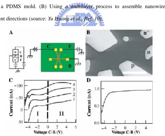
(A) “Fluidic alignment with surface-patterning techniques” for assembly using a PDMS mold. (B) Using a multilayer process to assemble nanowires in different directions (source: Yu Huang et al., Ref. 10).
Figure 2.2...16
n+–p–n SiNW bipolar transistors prepared from silicon nanowires. (A) Schematic structure and electrode of a silicon nanowire BJT device. (B) SEM image of a nanowire BJT. (C) The Ic–Vcb electronic characteristics of this BJT. (D) Plot of common base
current gain versus collector base voltage.
Figure 2.3...17
A field-effect transistor prepared from silicon nanowires. (A) Turn-on voltage of the silicon nanowire FET; the inset displays an SEM image of the FET device. (B) The Id–Vds electronic characteristics of this FET device (source: Yu Huang et al., Ref. 12)
Figure 2.4...17
A silicon nanowire logic gate. (A), (D), and (G) present the schemas, SEM images, and equal circuits of the logic gates, respectively. (B), (E), and (H) display the relationships between the input and output voltages. (C), (F), and (I) are truth tables (source: Yu
Huang et al., Ref. 12).
Figure 2.5...19
(A) Schematic illustration of the conversion of nanowire FETs into nanowire pH sensors. (B) Real-time detection of reversible protein binding (source: Yi Cui et al., Ref.
13).
Figure 2.6...20
(a) Optical image of the central region of a sensor test chip used for a DNA sensing study. (b, c) Representative SEM images displaying the SiNW bridging two contact leads (source: Z. Li et al., Ref. 15).
Figure 2.7...21
Field emission scanning electron microscopy images of the fabricated devices. There are two nanowires between the electrodes (source: R. Bashir et al., Ref. 16).
Electrical response of the device upon exposure to oxygen (dotted lines) and nitrogen (solid lines) gases (source: R. Bashir et al., Ref. 16).
Figure 2.9...24
Reversible nanoscale biosensing. A platinum silicide nanowire functionalized with single-stranded (capture) DNAs. Introduction of complementary (target) DNAs causes a rise in conductance across the nanowire. Rinsing with 55℃ buffer solution returned the conductance to its initial level.
Figure 3.1...29
Process flow chart for the fabrication of a platinum silicide nanowire device on a p-type <100> silicon wafer.
Figure 3.2...30
SEM image of the 80-nm polysilicon nanowire.
Figure 3.3...31
Cross-sectional view of the 60-nm platinum deposited on the wafer.
Figure 3.4...31
SEM image of the 40-nm-wide platinum silicide nanowire.
Figure 3.5...32
SEM image of the 20-µm-long platinum silicide nanowire.
Figure 3.6...32
AFM image of the 60-nm-wide platinum silicide nanowire.
Figure 3.7...34
Fluorescence microscopy image proving the existence of DNA on the Pt silicide nanowire.
Figure 3.8...35
The linker and DNA sequences.
The overall modification and DNA detection procedures.
Figure 4.1...37
Noise level of an HP-4156 semiconductor analyzer. The leakage current was ca. 50 fA.
Figure 4.2...38
The I–V curve of the 80-nm-wide and 6-µm-long polysilicon nanowire.
Figure 4.3...39
The I–V curve, obtained using an applied back-gate voltage (from –2 to +2 V), of the 80-nm-wide and 6-µm-long polysilicon nanowire.
Figure 4.4...40
SEM images of platinum ultra-thin films deposited on silicon wafers and annealed for 5 min at (a) 450, (b) 500, (c) 550, and (d) 600 °C.
Figure 4.5...41
The I–V curve of the 80-nm-wide and 6-µm-long polysilicon and platinum silicide nanowire.
Figure 4.6...41
SEM image of the 65-nm-wide and 6-µm-long platinum silicide nanowire.
Figure 4.7...42
SEM image of the polysilicon sidewall.
Figure 4.8...44
The conductance as a function of the RTA process temperature.
Figure 4.9...44
The conductances of 8-µm-long platinum silicide nanowires of different widths after RTA at 550 °C.
Figure 4.10...45
The conductances of 60-nm-wide platinum silicide nanowires of different lengths after RTA at 550 °C.
Figure 4.11...45
Producing a platinum silicide grain nanowire. Schematic diagram of polysilicon reacting with platinum, annealing at 550 ℃, and then washing with aqua regia solution to remove any unreacted platinum.
Figure 4.12...46
The concept of changing a platinum silicide grain nanowire’s electronic conduction properties through surface modification.
Figure 4.13...49
The standard deviation of conductance upon applying different back gate voltages to PtSi and polysilicon nanowires obtained after RTA at various temperatures.
Figure 4.14...49
The conductance of a platinum silicide nanowire (width: 38 nm; length: 6 µm) with repeat test.
Figure 4.15...50
The resistance of a platinum-silicide nanowire measured every five days.
Figure 4.16...50
The I–V curve of a platinum silicide nanowire (width: 40 nm; length: 4 µm) upon sweeping the applied voltage from 0 to 50 V.
Figure 4.17...54
The concept of modifying a platinum silicide nanowire’s surface. The inset presents the original I–V curves of modification steps (1)–(4).
Figure 4.18...54
The conductances obtained after modification steps (1)–(5).
Figure 4.19...55
The conductances, obtained after the modification steps, for wires in the presence of complementary and non-complementary DNA sequences.
Figure 4.20...55
The conductances, obtained after the modification steps, for wires having the same width but different lengths.
Figure 4.21...56
Variations of conductances measured and computed in the presence of different concentrations of target DNA.
Chapter 1 Introduction
1.1 General Introduction
“There is plenty of room on the bottom” is the title of a classic talk given on December 29, 1959, in which the great physicist Richard Feynman introduced a new field of physics to the annual meeting of the American Physical Society at the California Institute of Technology. Over 40 years ago, Feynman imagined a new physical world of ultra-small volumes and highlighted some difficulties that researchers might encounter when visiting it. His talk provided a vision for engineers and scientists to establish a new field, which—with subsequent developments in novel equipment and manufacturing skills—is know known as “nanotechnology.”
Nanotechnology has become a very popular word that is used to describe many types of research in which the characteristic dimensions are below ca. 1000 nm. For example, continuing improvements in lithography have resulted in the reduction of line widths to well below 1 micron. This kind of work is often called nanotechnology. Sub-micron lithography is clearly very profitable—ask anyone who uses a computer—but it is equally clear that conventional lithographic techniques will not let us prepare semiconductor devices in which individual dopant atoms are located at specific lattice sites. Although computer hardware capability has exhibited steady exponential growth for the last 50 years—and there is a fairly widespread belief that these trends are likely to continue for at least several more years—conventional lithographic techniques are beginning to reach their limits.
As semiconductor devices become scaled down to ever-smaller sizes within the nano-regime, a variety of technological and economic problems arise, the rules of classical physics give way to quantum mechanics, and the term “molecular-scale” becomes more accurate than “nanoscale.” At this point, the scaling of sizes that has
successfully reduced device features from the microscale to the nanoscale reaches its limits, and, therefore, alternative manufacturing methods, materials, device structures, and architectures are required. In this regime, the approach of fabricating nanoelectronic devices and interconnects using a combination of molecular and nanostructured materials with existing and emerging processing technologies promises to allow the continued miniaturization and enhancement in performance of the next generation of memory and logic chips.
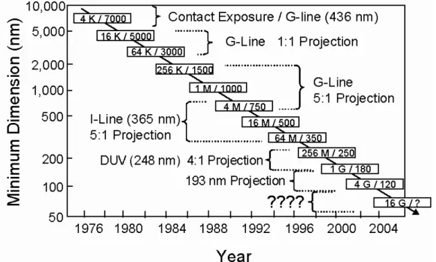
Figure 1.1 The semiconductor industry roadmap of memory technologies and the
associated lithographic technologies used to manufacture each generation of devices. Each box displays each device generation’s memory size and critical feature size (nm).
(nm)
1.2 Top-Down Nanotechnology
The lithography technology used to define each generation of circuit pattern has an enormous influence on the industrial manufacturing process. Figure 1.1 displays
the semiconductor industry roadmap of memory technologies and their associated lithographic technologies.[1] In the early days, the wavelength of the light source used was that of the G-line (436 nm), whose critical size was ca. 750 nm. Subsequently, the I-line (365 nm) was used. Currently, 193- and 157-nm radiation is the main source of exposure light. Table 1.1 lists the semiconductor industry roadmap of the key node indicators in the years 1999–2005 and three-year predictions for subsequent years through 2014.[2]
Table 1.1 Overall roadmap technology characteristics (ORTC) listed by technology node.
Year of First Product Shipment (Technology Generation) Technology
Node
Indicators 1999 2000 2001 2002 2003 2004 2005 2008 2011 2014
DRAM half-pitch (nm) 180 165 150 130 120 110 100 70 50 35 MPU gate length (nm) 140 120 100 85 80 70 65 45 32 22 MPU/ASIC half-pitch (nm) 230 210 180 160 145 130 115 80 55 40 ASIC gate length (nm) 180 165 150 130 120 110 100 70 50 35
Fabricating the high-performance integrated circuits requires increasingly shorter wavelengths of the radiation source to manufacture devices of decreasing critical sizes. Optical lithography technologies face a bottleneck for the formation of etched patterns over the next 10–15 years because the critical size of the patterns depends on the wavelength of the exposing radiation source.[3] When the wavelength
of the radiation source reaches its physical limit, it will become difficult and expensive to prepare pattern having, for example, 5–20-nm line widths. Despite the invention of some impressive techniques that increase process resolution—such as the use of phase shift masks (PSM),[4,5] off-axis illumination (OAI),[6] optical proximity correction (OPC)[7,8] and liquid immersion lithography (LIL)[9]—the limits of these methods to support process fabrication have been predicted to be ca. 65–90 nm. Therefore, emergency lithography technologies—including electron beam direct writing (EBDW),[10,11] extreme ultraviolet (EUV) lithography,[12] electron beam projection lithography (EPL),[13] electromagnetic radiation,[14] proximity X-ray lithography (PXL),[15] and ion beam projection lithography (IPL)[16]—have all been introduced for the fabrication of electronic devices. These approaches are all potential “next-generation lithography” (NGL) technologies, but currently they remain expensive and difficult to operate and implement.
Pattern transfer technologies can operate in two different ways, namely “top-down” and “bottom-up” approaches. Top-down fabrication is exemplified by conventional optical lithography and NGL techniques such as EBDW, EUV, EPL, PXL, and IPL, but “soft lithography” and “nanoimprinting” are also key technologies for preparing nanosized patterns. Figure 1.2 presents the concept of soft lithography,[17] which is based on the use of elastomeric polymers to transfer a pattern from a master to a large number of copies having single-layer structures. Soft lithography comprises a number of different fabrication processes, including microcontact printing (CP), replica molding (REM), microtransfer molding (TM), micromolding in capillaries (MIMIC), and solvent-assisted micromolding (SAMIM). Poly(dimethylsiloxane) PDMS molds are usually used as materials for transfering patterns to the substrates. Soft lithography utilizes the CP of a self-assembled monolayer (SAM) or organic material to define the nanosize pattern. Furthermore, soft lithography has great potential because it does not require expensive equipment or a high-quality clean room, but it is ineffective for fabricating multi-layer structures or for allowing precision alignment.
Nanoimprinting (Figure 1.3) is an emerging lithographic technology that has promise for the high-throughput patterning of nanostructures. Based on the mechanical embossing principle, the nanoimprinting technique can achieve pattern resolutions beyond the limitations set by light diffraction or e-beam scattering in other conventional techniques. The nanoimprinting lithography (NIL) technique[18,19] involves two main steps. The first requires electron beam direct writing on an e-beam resist, followed by the deposition of metal and reactive ion etching, to define a pattern on a mold. Secondly, the mold is imprinted upon the substrate, which has a coated resist, and then metal deposition and RIE etching allows the preparation of 2D or 3D nanostructures (Figure 1.4). The key to successful nanoimprinting is preventing
residual mold attachment after it is removed from the resist coating substrate during the imprinting process.
Figure 1.3 The nanoimprinting process (source: Appl. Phys. Lett. 67 (1995)
3114–3116).
The lithographic methods described above all have resolutions of 100 nm or better, but each of these methods has its limitations: diffraction effects during optical lithography, proximity effects during EBDW and EPL, difficulties in mask fabrication for X-ray and EUV lithographies, difficulties in aligning and preparing vertical structures during soft lithography and NIL, and stochastic space charge during ion projection lithography.
1.3 Bottom-Up Nanotechnology
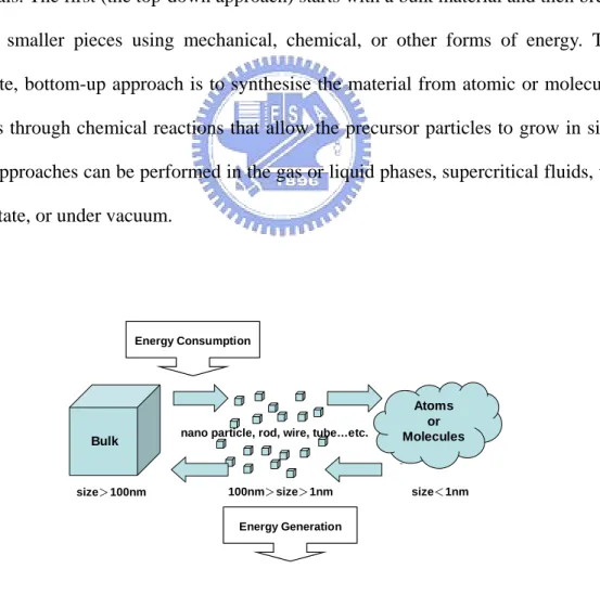
Figure 1.5 displays the two general methods available for producing nanosize materials. The first (the top-down approach) starts with a bulk material and then break it into smaller pieces using mechanical, chemical, or other forms of energy. The opposite, bottom-up approach is to synthesise the material from atomic or molecular species through chemical reactions that allow the precursor particles to grow in size. Both approaches can be performed in the gas or liquid phases, supercritical fluids, the solid state, or under vacuum.
Bulk
Atoms or Molecules
size>100nm 100nm>size>1nm size<1nm
Energy Consumption
Energy Generation nano particle, rod, wire, tube…etc.
Figure 1.5 Two basic approaches toward the fabrication of nanomaterials: top-down
Section 1.2 introduced some of the fabrication methods that may be used to shrink the sizes of electronic devices. In contrast, we can also fabricate nano-electronic devices by using the bottom-up method. The term “bottom-up” means that the nano-components (particles, nanotubes, and nanowires) are synthesized from single molecules, whereas the top-down process fabricates these nano-components from bulk materials.
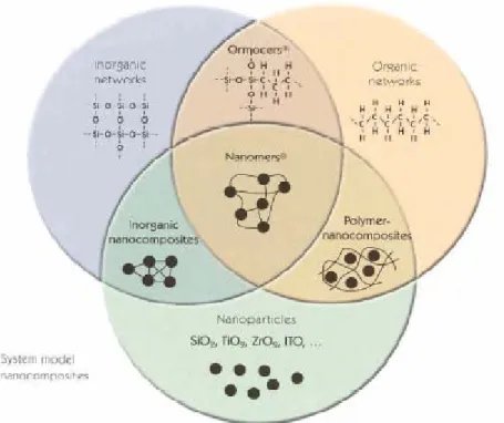
Figure 1.6 System model for nanocomposites produced by the sol–gel process
(source: Fraunhofer IST).
Methods for producing nanoscale materials from atoms are chemical processes based on transformations that occur in solution; e.g., sol–gel processing, chemical vapor deposition (CVD), plasma or flame spraying synthesis, laser pyrolysis, and atomic or molecular condensation. These chemical processes rely on the availability of appropriate “metal–organic” molecules as precursors. Sol–gel processing is different from other chemical processes because it requires a relatively low processing
temperature, which makes it a cost-effective and versatile technique (Figure 1.6). In spraying processes, the flow of reactants (gas or liquid in the form of aerosols, or mixtures of both) is introduced to a high-energy flame produced, for example, by a plasma spraying apparatus or a carbon dioxide laser. The reactants decompose and particles are formed in a flame by homogeneous nucleation and growth. Rapid cooling results in formation of nanoscale particles.
Chemical processes—that are based on transformations in solution—toward materials include sol–gel processing, hydro- or solvo-thermal syntheses, metal organic decomposition (MOD), and vapor phase chemical vapor deposition (CVD). Most chemical routes rely on the availability of appropriate “metal–organic” molecules as precursors. Of the various precursors of metal oxides, the metal β-diketonates, metal carboxylates, and metal alkoxides are the most versatile. They are available for nearly all elements; cost-effective syntheses from cheap feedstocks have been developed for some of these materials.
Two general methods are available for controlling the formation and growth of these nanoscale materials. One, “arrested precipitation,” depends on either the exhaustion of one of the reactants or the introduction of a chemical that would block the reaction. The other method uses templates to physically restrict the volume available for growth of the individual nanoscale materials.
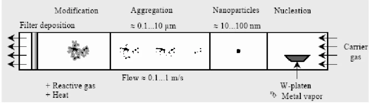
Figure 1.7 displays the principle of atomic or molecular condensation, which is used primarily for metal-containing nanoparticles. A bulk material is heated under vacuum to produce a stream of vaporized and atomized matter that is directed to a chamber containing either an inert or reactive gas atmosphere. Rapid cooling of the metal atoms—through collisions with gas molecules—results in the condensation and formation of nanoparticles. Metal oxide nanoparticles are produced if a reactive gas, such as oxygen, is used.
The theory of gas phase condensation for the production of metal nanopowders is well known; it was first reported in 1930.[20] Gas phase condensation uses a vacuum chamber comprising a heating element, the metal to be transformed into the nano-powder, powder collection equipment, and vacuum hardware.
Figure 1.7 The inert gas condensation method for producing nanoparticulate material
(source: FHG-IFAM, Bremen).
The process utilizes a gas, which is typically inert, at pressures high enough to promote particle formation, but also low enough to allow the production of spherical particles. The metal is introduced onto a heated element and is rapidly melted. The metal is quickly heated to a temperature far above its melting point, but less than its boiling point, so that an adequate vapor pressure is achieved. Gas is introduced into the chamber continuously and removed by the pumps so that the gas transfers the evaporated metal away from the hot element. Nanometer-sized particles form as the gas cools the metal vapor. These particles are in liquid form because they are still too hot to solidify. The liquid particles collide and coalesce in a controlled environment so that the particles grow to specific size and remain spherical and have smooth surfaces. When the liquid particles are further cooled under controlled conditions, they become solid and no longer grow. At this point the nanoparticles are very reactive; they must be coated with a material that prevents further interaction with
other particles (agglomeration) or with other materials.
Nanoparticles of a wide range of materials—including a variety of organic and biological compounds, inorganic oxides, metals, and semiconductors—can be processed using chemical self-assembly techniques (Meier et al. 2000, Zhang et al. 2002, Shimizu et al. 2003, Shimomura et al. 2000, Tomalia et al. 1999, Fendler et al. 2001). These techniques exploit the selective attachment of molecules to specific surfaces, biomolecular recognition, and self-ordering principles (e.g., the preferential docking of DNA strands with their complementary base pairs) in addition to the well-developed chemistry for attaching molecules onto clusters and substrates [e.g., thiol (–SH) end groups]; other techniques include reverse micelle, sonochemical, and photochemical syntheses to realize 1D, 2D, and 3D self-assembled nanostructures. The molecular building blocks act as parts of a jigsaw puzzle that join together in perfect order without the presence of an obvious driving force. Long-term and visionary nanotechnological concepts go far beyond these first approaches, particularly for the development—by means of molecular nanotechnology—of biomimetic materials that have the ability to self-organize, self-heal, and self-replicate. One objective here is to prepare combinations of synthetic and biological materials, architectures, and systems to imitate biological processes in technological applications. At present, the field of nanobiotechnology remains at the stage of basic research, but it is regarded as one of the most promising future research fields (European Commission 2001).
1.4 Motivation
When we talk about “nanotechnology”—building structures with atoms and molecules and getting them to do what we want—it is obvious that we mean very small structures. Nowadays, one approach to nanotechnology considers if it is
possible to examine how biological systems perform molecular processes and signaling in the living body. One molecule that directs its own synthesis is deoxyribonucleic acid (DNA), which is almost an entire nano-specialty in itself. Single-stranded DNA binds strongly only to other single DNA strands possessing a specific sequence of nucleotides; this property allows them to be used to position electrical wires and contacts precisely, without the need for direct manipulation.
Current DNA sensors are based on radiolabeling and fluorescence labeling techniques. These methods are sensitive, but they suffer the drawback of requiring radioisotopes that have a relatively long half-life, such as 32P. Exposure of a body to
32
P radioisotopes for a long time damages the normal cells of organs. This method also requires expensive monitoring equipment for optical detection, as well as the sample DNA, which is often fixed onto a membrane for hybridization with the probe. In addition, we must consider the expensive biological agents and time required to complete the DNA polymerase chain reactions (PCR)[21] that are necessary to obtain good analytic results. In the other words, conventional methods of DNA detection spend a lot of time and money.
Many research groups worldwide are focused on DNA detection through electrical signaling with the goal of rapidly diagnosing specific series of DNA that lead to diseases such as cancer, diabetes, cardiopathy and hypertension. The two most prominent groups are those of Chad A. Mirkin’s team at Northwestern University and Charles M. Lieber’s team at Harvard University. In Mirkin’s group, gold nanoparticles have been used to modify thiol ssDNA as a probe to hybridize with another capture ssDNA and target ssDNA in the gap. Silver ions can be reduced on these gold nanoparticles if the DNA is fully complementary, which decreases the resistance between the two electrodes.[22] Subsequently, C. C. Chen et al. proposed multilayer gold particle DNA sensors[23] and discussed their quantum conductivity behavior.
For sensing purposes, such zero-dimensional nanoparticles are difficult to arrange well for repetitive, real-time detection. On the other hand, a number of studies of 1D nanowire sensors have been reported. The Lieber group has proposed the use of silicon nanowires as powerful sensors for biological, chemical, and PH uses.[24,25] Furthermore, 2D sensors have also been studied.[26] These 1D and 2D sensors operate under the theory that the charge distribution changes when DNA or a chemical becomes attached to the sensor (nanowire or channel) area; when the charge distribution of the nanowire or channel changes, the conductance of the device changes. One rule of MOSFET research is that sensitivity is improved upon shrinking the channel width. When an FET device channel width is on the nano-scale, the device can be considered to be a nanowire sensor.
Although the results described above are inspiring, the fabrication methods that have been used to create these devices are typically incompatible with modern semiconductor manufacturing techniques so that their large-scale integration remains problematic.[27] In work described in this Thesis, platinum silicide nanowires were defined by electron beam lithography (EBL) and fabricated using a standard semiconductor process. When performing rapid thermal annealing under different temperatures, the platinum silicide grain sizes changed and influenced the conductance of their nanowires. The surfaces of platinum silicide nanowires were then modified to allow the attachment of DNA. The conductance of the nanowires rose when single-stranded DNA was attached. Once the complementary DNA hybridized with the surface, the conductance rose yet again. Upon denaturation, the conductance of the nanowire returned back to that of the single-strand-appended DNA surface. These findings highlight the potential of this system for use as a DNA hybridization sensor and for its integration into the processes used for the mass production of semiconductors.
1.5 Organization of Thesis
This Thesis reports platinum silicide nanowires—manufactured using a standard semiconductor process—that behave as novel DNA sensors. We fabricated the nanowires, which have high sensitivity, on inexpensive poly-Si/oxide/silicon SOI-like structured wafers. Label-free single-stranded DNA was then modified onto the nanowires using commercially available chemicals and solvents of reagent-grade quality that required no further purification. A number of challenges had to be overcome during this project, including defining the pattern, shrinking the nanowires, forming the platinum silicide, modifying the label-free DNA, and detecting the electrical signal. This study required knowledge of biology, biochemistry, and materials science and of electron beam lithography, nanofabrication, rapid thermal annealing, and self-assembly techniques.
Chapter 1 provides a general overview of the “top-down” and “bottom-up” approachs to “nanotechnology”, and the motivation behind biomolecule (DNA) detection. Chapter 2 introduces literature surveys of silicon nanowires, fabrication tools, and experimental ideals. Chapter 3 presents details of the fabrication processes and the modification steps. Chapter 4 not only discusses the electrical properties of polysilicon and platinum silicide nanowires but also demonstrates their application toward DNA detection. The final two Chapters summarize the contributions of this research and address potential future work, respectively.
Chapter 2 Review and Design Concepts
2.1 Silicon Nanowire (Bottom-Up)
The synthesis and characterization of silicon nanowires has recently attracted a great deal of attention. Silicon nanowires have been synthesized in a bottom-up process using a vapor–liquid–solid (VLS) mechanism;[1] the diameters of these nanowires can be controlled by varying the ambient gases[2] and pressure[3] and by employing[4] gold nanoclusters. The VLS method displays good diameter-control and the mass production of nanowires has been described in detail by Wagner and Ellis.[5,6] Silicon nanowires have also been demonstrated to function as simple field-effect transistors.[7,8] These results suggest that silicon nanowires can be used as critical components in nanoelectronic devices.
The assembly of these nanowires into devices remains a critical task that has limited the evolution of applications for nanowire devices. Lieber and co-workers developed[9] a new alignment method, which they named “fluidic alignment with surface-patterning techniques,” to accomplish the large-scale hierarchical organization of nanowire arrays for integrated nanosystems.[10] Figure 2.1 displays a schematic illustration of a fluidic channel structure. The authors demonstrated that nanowires could be assembled into parallel arrays with controlled average separation; a fluidic channel was fabricated using the poly(dimethylsiloxane) (PDMS) mold so that it was also possible to control the periodicity. In addition, complex arrays of crossed nanowires can be prepared in a layer-by-layer assembly when using different flow directions sequentially. This assembly process allows nanowires to be aligned accurately within a desired area; field-effect and bipolar transistors have been prepared from silicon nanowires (Figures 2.2 and 2.3, respectively).[11,12] In addition, this assembly method has been used to prepare nano-scale logic gate devices (OR,
AND, and NOR gates; Figure 2.4) from silicon nanowires.[12]
Figure 2.1 (A) “Fluidic alignment with surface-patterning techniques” for assembly
using a PDMS mold. (B) Using a multilayer process to assemble nanowires in different directions (source: Yu Huang et al., Ref. 10).
Figure 2.2 n+–p–n SiNW bipolar transistors prepared from silicon nanowires. (A) Schematic structure and electrode of a silicon nanowire BJT device. (B) SEM image of a nanowire BJT. (C) The Ic–Vcb electronic characteristics of this BJT. (D) Plot of
A B
Figure 2.3 A field-effect transistor prepared from silicon nanowires. (A) Turn-on
voltage of the silicon nanowire FET; the inset displays an SEM image of the FET device. (B) The Id–Vds electronic characteristics of this FET device (source: Yu Huang
et al., Ref. 12).
Figure 2.4 A silicon nanowire logic gates. (A), (D), and (G) present the schemas,
SEM images, and equal circuits of the logic gates, respectively. (B), (E), and (H) display the relationships between the input and output voltages. (C), (F), and (I) are truth tables (source: Yu Huang et al., Ref. 12).
Silicon nanowires not only display good performance as electronic devices, but they also function as chemical and biological sensors. In a recent issue of Science, Cui et al.[13] reported (Figure 2.5) the conductance behavior of nanofabricated doped silicon nanowires functionalized with organic molecules and biomolecules. Their results indicate that these functionalized nanowires may provide a new type of platform for the sensitive and selective sensing of chemical and biological agents. The small size and capability of these semiconductor nanowires lead to their sensitive, label-free, and real-time detection of a wide range of chemical and biological species (e.g., DNA and proteins), which could be exploited for array-based screening and in vivo diagnostics. What is particularly exciting about these results is the potential for realizing a nanoscale interface that bridges solid state electronics and true molecular-scale processes, not only for its selective detection capabilities but also for its eventual use in extra- and intercellular measurement.[14]
Figure 2.5 (A) Schematic illustration of the conversion of nanowire FETs into
nanowire pH sensors. (B) Real-time detection of reversible protein binding (source: Yi
Cui et al., Ref. 13).
Although basic nanowire electrode devices appear to be similar to standard monolithic integrated circuit devices (i.e., those prepared on a single substrate), there are important differences. The nanowires are grown off-chip and then dispersed onto a wafer; contact leads are then aligned individually to randomly placed nanowires. The large-scale integration of this technique is limited by the hybrid and serial (versus monolithic and parallel) fabrication of devices, with concurrent issues of yield and uniformity.
2.2 Silicon Nanowire (Top-Down)
Bottom-up approaches to nanotechnology are popular, but most of the existing studies based on bottom-up nanostructures are limited by their complex integration processes, which require transfer and positioning of individual nanostructures and the forming of reliable ohmic contacts. Furthermore, controlling the doping concentrations in self-assembled semiconducting nanostructures remains a challenge, and the fabrication of high-density sensor arrays is also very difficult. Therefore, top-down processes for fabricating electronic devices are still being developed by using techniques such as electron beam lithography (EBL) and dry etching. Z. Li et al. of Hewlett–Packard have fabricated a 50-nm-wide single-crystal silicon nanowire on
an SOI wafer by using electron bean lithography.[15] These authors demonstrated the detection of DNA molecules, based on their intrinsic charge, by using silicon nanowires fabricated by standard top-down semiconductor processes. This method creates a pathway for fabricating high-density, high-quality, well-organized nanoscale sensors that can be integrated into silicon-based signal processing and communication circuits (Figure 2.6). Highly sensitive and sequence-specific DNA sensors have been demonstrated on silicon nanowires that possess single-stranded DNA probes covalently immobilized onto their surfaces. For a 12-mer oligonucleotide probe, a 25 pM solution of target DNA could be detected with excellent discrimination against a single base mismatch.
Figure 2.6 (a) Optical image of the central region of a sensor test chip used for a
DNA sensing study. (b, c) Representative SEM images displaying the SiNW bridging two contact leads (source: Z. Li et al., Ref. 15).
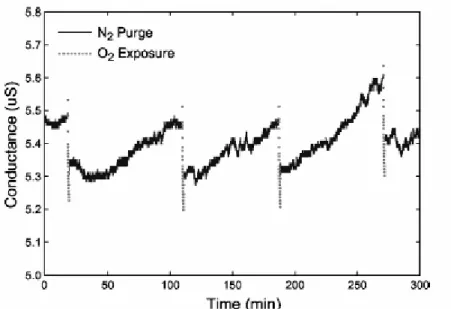
R. Bashir and co-workers have also described the fabrication and initial testing of a silicon nanowire sensor that they realized using top-down microelectronics processing techniques.[16] They used a process known as confined lateral selective epitaxial growth (CLSEG)[17] to obtain single-crystal silicon nanoplates as thin as 7 nm and nanowires as small as 40 nm in diameter at precise locations (Figure 2.7). This method allows the realization of truly integrated dense sensor arrays. Initial testing of the device indicated its sensitivity towards ambient oxygen gas, and suggested the possibility of using these sensors for chemical and biological detection (Figure 2.8).
Figure 2.7 Field emission scanning electron microscopy images of a fabricated device.
Figure 2.8 Electrical response of the device in Fig. 2.7 upon exposure to oxygen
(dotted lines) and nitrogen (solid lines) gases (source: R. Bashir et al., Ref. 16).
2.3 Experimental Features
The previous two Sections introduced silicon nanowires that have been fabricated using bottom-up and top-down processes. The results demonstrated by these authors are outstanding and exciting, but the methods for fabricating these systems still display many shortcomings. New approaches to overcoming these problems must be discovered. This Thesis provides a comparison of the new concepts provided by the our experimental findings with the methods described in the reference literature. The following points highlight the features and concepts of this thesis.
First, we believed that it may be possible to deposit silicon dioxide and polysilicon sequentially to replace the silicon-on-insulator (SOI) wafer. This replacement will lower costs because SOI wafers are ten times as expensive as bare silicon wafers. Thus, we defined the nanowire pattern onto polySi/SiO2/Si wafers by
using electron beam direct writing. After the patterns were defined, we shrank the width of the nanowires through a wet etching process.
top of the polysilicon nanowire and formed platinum silicide by RTP annealing to replace ion implantation. The electron conduction mechanism is discussed in Chapter 4.
Thirdly, DNA-based sensors described to date in the literature—from the efforts of the Lieber, Mirkin, and HP groups—have all featured immobilized single-stranded DNA on the substrate or nanowire. These DNA strands have always been attached to the surfaces after previously modifying one of their functional groups; e.g., Mirkin’s approach to functionalizing DNA strands with thiol groups at their 5´ or 3´ termini for the purpose of coupling them to gold nanoparticles. We have found, however, a method to directly couple DNA molecules’ 5´ termini with amino groups in an aqueous CDI/imidazole solution. This approach avoids the need for preparing chemically modified nucleic acids, which reduces production costs.
Finally, our experiments utilized commercial equipment available at the National Nano Device Laboratories for our front-end nanowire fabrication. Thus, our platinum silicide nanowire device is compatible with standard semiconductor fabrication processes.
2.4 Detection Concepts
If a silicon nanowire acts as a channel between source and drain electrodes, its conductance changes depending on the gate voltage applied. Thus, we modified APTMS on the platinum silicide to behave as a linker between the surface-immobilized single-stranded DNA and the nanowire. This nanowire can detect the complementary single-stranded DNA of the immobilized DNA strand on its surface. The conductance of the nanowire rose after the DNA immobilization, and then it rose again after the complementary DNA strand hybridized with its surface-bound congener. Upon denaturation of the double-stranded DNA, the
conductance of the nanowire returned back to the level it displayed for the immobilized single-stranded DNA; Figure 2.9 provides a diagram of the concept.
I1 I2 I1 nanowire C o nd uc ta nc e Time
Capture DNA Target DNA
Figure 2.9 Reversible nanoscale biosensing. A platinum silicide nanowire
functionalized with single-stranded (capture) DNAs. Introduction of complementary (target) DNAs causes a rise in conductance across the nanowire. Rinsing with 55℃ buffer solution returned the conductance to its initial level.
2.5 Electron Beam Lithography (EBL)
Electron beam lithography (EBL) is a well-established high-resolution patterning technique in which highly accelerated (10–100 keV) electrons are focused into a narrow beam and used to expose electron-sensitive resists. Higher energy causes strong particle scattering in materials and, hence, it ruins the resolution of the tools. In addition to the relatively expensive cost of the equipment, conventional focused beam techniques offer only a direct writing capability. This tool can focus charged particle beams to a size as low as 10 nm. The critical size of the e-beam system at the National
Nano Device Laboratories is, however, only 100 nm, and, therefore, we needed to perform additional shrinking processes.
Chapter 3 Experimental Section
A number of technologies for the fabrication of silicon nanowires, including both bottom-up and top-down processes, were introduced in the previous Chapter. This Chapter describes the preparation of the nanowire-like structures of polycrystalline silicon. We fabricated polycrystalline silicon nanowires (PSNWs) through electron beam lithography (EBL) and shrank them by using isotropic wet etching. These fabrication processes all employed commercial semiconductor equipment located in the National Nano Device Laboratories.[1]
3.1 General Information
All reagents and solvents were of reagent-grade quality, purchased commercially, and used without further purification, unless otherwise noted. The experimental reagents included:
1. Deoxyribonucleic acids (OPC grade; Purigo Biotech) Fluorescence Capture DNA (MW 8160)
5´-ATC CTT ATC AAT ATT TAA CAA TAA TCC-3´ Complementary target DNA (MW 8391)
3´-TAG GAA TAG TTA TAA ATTT GAA ATT AGG-5´ Non-complementary target DNA (MW 8251)
3´-AAG CAC GGT CCT TTA TGC TCC GGA TGC-5´
2. (3-Aminopropyl)trimethoxysilane [APTMS; H2N(CH2)3Si(OCH3)3; 97% purity;
Sigma].
APTMS was used to modify the exposed SiO2 surface on the platinum silicide
nanowire. The methoxy functional groups of APTMS are displaced through covalent bond formation between the hydrophilic hydroxyl groups of the SiO2
surface and the silicon atom of APTMS; this process leads to the formation of a molecular layer of amino groups for bonding with DNA molecules.
3. 2-Morpholinoethanesulfonic acid (MES; C6H13NO4S; 99% purity; Sigma).
MES is an acid buffer solution. In this study, MES was prepared as a 50 mM solution in DI water and then mixed with 0.1 M imidazole and 0.1 M CDI solutions for immobilizing nucleic acids onto the silanized surface.
4. Imidazole (C3H4N2; 99% purity; Sigma).
Imidazole was mixed with the MES buffer and CDI cross-linker for immobilizing DNA onto the SiO2 surface.
5. N-Cyclohexyl-N´-[2-(N-(methylmorpholino)ethyl]carbodiimide-4-toluene sulfonate (CDI; C14H25N3O·C7H8SO3; 99% purity; Sigma).
CDI was used to link the nucleic acid molecules to the amino groups bound on the SiO2 surface.
6. Sulfuric acid (H2SO4; 98% purity; Sigma).
Sulfuric acid was mixed with hydrogen peroxide in a 3:1 ratio and used to lift off the NEB resist pattern exposed to high-energy radiation from the electron beam after the polysilicon was etched using a TCP 9400SE dry etching system.
7. Sodium hydroxide (NaOH; 98% purity; Sigma).
10 M Sodium hydroxide in DI water was used to adjust the pH of the HEPES/EDTA buffer solution.
8. N-2-Hydroxyethylpiperazine-N´-2-ethanesulfonic acid (HEPES; C8H18N2O4S;
99% purity; CALBIOCHEM).
HEPES, a biological buffer solution, was mixed with EDTA to conserve the target DNA molecules during their hybridization reactions with capture strands. 9. Ethylenediaminetetraacetic acid [EDTA; (HOOCCH2)2NC2H4N(CH2COOH)2;
EDTA was used to capture cations, such as Mg2+ and Ca2+, that can induce certain enzymes to digest and destroy the structures of nucleic acids during experimental processes.
10. Phosphate-buffered saline tablets (PBS; CALBIOCHEM).
PBS, a biological buffer solution, was used to increase the selectivity of the DNA chips by washing away any non-hybridized nucleic acids and non-complementary target DNA sequences.
3.2 Experimental Steps
All experiments were performed using single-crystalline p-type <100> silicon wafers. There were four major steps: (1) fabrication of polycrystalline silicon nanowires (PSNWs), (2) deposition of the platinum film and formation of platinum silicide, (3) self-assembly of the linker layer and attachment of DNA strands to the nanowire, (4) detection of complementary and mismatched single-stranded DNA sequences.
3.2.1
Fabrication of polycrystalline silicon nanowires (PSNWs)
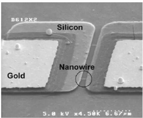
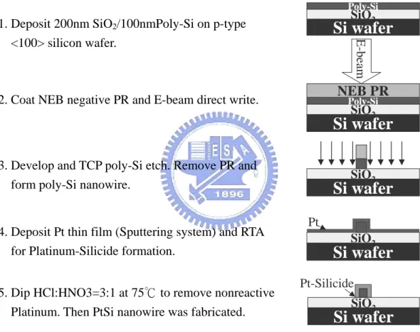
Figure 3.1 illustrates the process procedure. Single-crystalline p-type <100> silicon wafers were used. Standard RCA cleaning was followed by deposition using a thermal oxidization furnace of a silicon dioxide film (200 nm) as the isolation layer. Low-pressure CVD was used to deposit a polysilicon layer (100 nm). The electron beam resist NEB 22-A was spin-coated using a TEL CLEAN TRACK MK-8. Next, a Leica WePrint 200 e-beam writer was used to pattern nanowires of various widths and lengths and the contact pad. 2.38% Tetramethyl ammonium hydroxide (TMAH) solution was used for developing. Because of the resolution of the Leica e-beam direct writer, we needed to choose an optimal exposure dose. The polysilicon layer was
etched using a TCP (LAM TCP 9400SE) polysilicon etcher and then the resist was removed by treatment with thermal ozone (FUSION OZONE ASHER) and dipping the wafer in H2O2/H2SO4 (3:1) for 20 min. This procedure produced 80-nm
polysilicon nanowires (Figure 3.2). An additional wet etching process was performed to achieve sub-80-nm nanowires; i.e., NH4OH/H2O2/H2O (0.25:1:5) was
applied to shrink the 80-nm nanowires to 50–60-nm widths.
Si wafer
SiO2 Poly-SiSi wafer
SiO2 Poly-Si NEB PR E -b ea mSi wafer
SiO2Si wafer
SiO2 PtSi wafer
SiO2 Pt-Silicide1. Deposit 200nm SiO2/100nmPoly-Si on p-type
<100> silicon wafer.
2. Coat NEB negative PR and E-beam direct write.
3. Develop and TCP poly-Si etch. Remove PR and form poly-Si nanowire.
4. Deposit Pt thin film (Sputtering system) and RTA for Platinum-Silicide formation.
5. Dip HCl:HNO3=3:1 at 75℃ to remove nonreactive Platinum. Then PtSi nanowire was fabricated.
Figure 3.1 Process flow chart for the fabrication of a platinum silicide nanowire
device on a p-type <100> silicon wafer.
3.2.2 Deposition of a Platinum Film and the Formation of the Platinum
Silicide
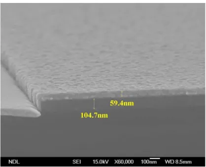
Platinum films (60 nm) were deposited on the pre-patterned polysilicon nanowire wafers using an ULVAC SBH-3308 RDE sputter system (Figure 3.3). The wafers
were then annealed at various temperatures (400–600 °C at 50 °C per step) using a HeatPulse 610 rapid thermal processing system to form the platinum silicide on the polysilicon nanowire. The resulting wafers were immersed in HNO3/HCl/H2O
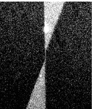
solution (1:3:4) at 75 °C to remove and unreacted platinum. After this step, the platinum silicide nanowires were observed to have final line widths that had shrunk to ca. 30%. Figures 3.4 and 3.5 present the nanowires having the minimum line width (a 38-nm nanowire) and the maximum line length (20 µm). Figure 3.6 displays an AFM image of a 60-nm-wide PtSi nanowire.
Figure 3.3 Cross-sectional view of the 60-nm-thick platinum layer deposited on the
wafer.
Figure 3.5 SEM image of a 20-µm-long platinum silicide nanowire.
Figure 3.6 AFM image of a 60-nm-wide platinum silicide nanowire.
3.2.3 Self-Assembly of a Linker Layer Between the DNA and the
Nanowire
For biosensing purposes, the nanowire surface was modified by attaching DNA strands. The PtSi surface was first modified with amino groups using APTMS. The
samples were prepared[2] by using the following three processes:
<1.> Pre-cleaning the surface of the platinum silicide nanowire.
The samples were rinsed with DI water and then they were immersed in 2.5% potassium dichromate in 15% nitric acid for 30 min at 56 °C. The samples were then washed with 0.02 N HCl and DI water.
<2.> Modifying with the APTMS linker.
The samples were immersed for 30 min at 37 °C in 10% aqueous APTMS solution whose pH had been adjusted to 3.5 using HCl. The samples were then rinsed with DI water and dried by hot baking at 110 °C.
<3.> Immobilized single-stranded DNA sequences.
The selective immobilization technique of Ghosh and Musso[3] was used to bind the terminal 5´ phosphate groups of the oligonucleotides to the amino groups on the surface. A solution was prepared of water-soluble 0.1 M CDI and
0.1 M imidazole. This solution was mixed with 1 nM single-stranded capture DNA solution, and then the wafers were immersed in the mixture solution for 16 h to ensure complete bonding. After being rinsed with DI water, the sample was immersed in 0.1*SSC solution at 37 °C for 10 min; this procedure was repeated twice. The wafer was then washed with DI water and PBS solution, purged with N2, and dried by hot baking. A fluorescence-labeled single-stranded DNA was
prepared for use in a control experiment to determine, using fluorescence microscopy, whether the DNA strands were present on the PtSi nanowires (Figure 3.7).
Figure 3.7 Fluorescence microscopy image proving the existence of DNA on the PtSi
nanowire.
3.2.4 Detection of Complementary and Non-complementary ssDNA
After surface modification and the bonding of capture DNA, strands of target DNA were applied to hybridize with the immobilized capture DNA. The sequences of target DNA that were used were both complementary and mismatched with respect to the capture DNA. Figure 3.8 presents the complementary and mismatched DNA sequences. A 10 mM HEPES (J.T. Baker Chem. Co.) solution was prepared and 5 mM EDTA buffer was used to adjust its pH to 6.6 (i.e., to form the HEPES buffer). The 27-mer target DNA (1 nM) was de-aerated in the prepared HEPES buffer. The wafers were immersed in the buffer for ca. 2 h for DNA detection, washed with 0.3 M PBS buffer to remove any excess target DNA, and then dried under N2. The resulting chip
was washed with 0.3 M PBS buffer again to ensure that the target DNA had indeed hybridized with the capture DNA. Finally, the chips were immersed in DI water for a few seconds and then dried under a N2 purge and stored in a low-vacuum chamber.
Linker:
Aminopropyltrimethoxysilane (APTMS)
Capture DNA:
5´ ATC CTT ATC AAT ATT TAA CAA TAA TCC 3´ Complementary DNA:
3´ TAG GAA TAG TTG TAA ATT GTT ATT AGG 5´ Non-complementary DNA:
3´ AAG CAC GGT CCT TTA TGC TCC GGA TGC 5´
Figure 3.8 The linker and DNA sequences.
The electrical behavior of the DNA sensors was characterized using an HP 4156A semiconductor parameter analyzer. We measured the conductance of the platinum silicide nanowire after every step of the modification procedure. In the hybridization experiments, the conductances of the nanowires were measured in the presence of both the complementary and mismatched DNA. After measuring the electrical characteristics, the chips were washed with PBS solution at 55 °C to denature the complementary hybridized double-stranded DNA. The electrical characteristics were then measured once again. Figure 3.9 displays the overall procedure.
Capture DNA Pt-Silicide nanowire Si Si Si OH OH OH Pt Pt O O O Si NH2 O O O Si NH O O O P O AT C CT T AT C AA T AT T T A A C A A T A A T C C O O O Si NH O O O P O A T C C T T A T C A A T A T T T A A C A A T A A T C C TA G G AA T A G T T G T A A A T T G TT A TT A G G Target DNA Modify APTMS Capture DNA Immobilize Detect Target DNA CDI+Imidazole HEPES+EDTA
DNA Detection
Scheme
Chapter 4 Results and Discussion
We have successfully fabricated nanowires of polycrystalline silicon and platinum silicide on silicon wafers. The platinum silicide nanowire device is similar in structure to a planar field effect transistor (FET); the conductive channel is replaced by the platinum silicide nanowire so that the conductance can be controlled by applying a backgate voltage. We characterized the electrical behavior of the nanowire device and its behavior as a DNA sensor at room temperature using an HP 4156A semiconductor parameter analyzer. Prior to sample measurement, the noise level of the electrical analyzer was measured to be ca. 50 fA; when a 1-V potential was applied (Figure 4.1), we estimated the conductance to be 0.05 pS. The results are discussed in the following paragraphs.
-3 -2 -1 0 1 2 3 -400.0f -200.0f 0.0 200.0f 400.0f Curren t (A) Voltage(V)
Figure 4.1 Noise level of an HP-4156 semiconductor analyzer. The leakage current
4.1 Electrical Properties of Polysilicon Nanowires
Although the polysilicon nanowires themselves were not the main focus of our study, it was still necessary to perform some measurements with them to clarify our findings. Prior to platinum silicide formation, we measured the I–V characteristics of a polysilicon nanowire of 80 nm width and 6 µm length (Figure 4.2). We determined the approximate conductance of the polysilicon nanowire to be 2.5 pS when applying a potential (Vds) of 1 V. After applying a backgate voltage (Vbg), the polysilicon
nanowire displayed an accumulation mode at negative Vbg and a depletion mode at
positive Vbg (Figure 4.3). As a result, we postulate that the polysilicon nanowire
behaves as a p-type conductive channel that is sensitive to applied charge. Next, we compared the effect of charge on a polysilicon nanowire with that of a platinum silicide nanowire. -1.0 -0.5 0.0 0.5 1.0 -20.0p -10.0p 0.0 10.0p 20.0p I ds (A) Vds(V)
0.5 1.0 1.5 2.0 2.5 0.0 10.0p 20.0p 30.0p Ids (A ) Vds (V) - 2V - 1V 0V +1V +2V Vbg
Figure 4.3 The I–V curve, obtained using an applied back-gate voltage (from –2 to +2
V), of an 80-nm-wide and 6-µm-long polysilicon nanowire.
4.2 Electrical Properties of Platinum Silicide Nanowires
The platinum silicide nanowires in this experiment were prepared using the RTA process at different temperatures in an effort to increase the conductance of the nanowires for their use as biomolecule sensors. First, we deposited ultra-thin platinum films (5 nm) on silicon wafers and anneal them at 400, 450, 500, and 550 °C. The platinum film separated into isolated platinum islands after annealing. The shapes of the isolated islands tended to be rounder at higher temperatures. After RTA, we investigated the surface of the ultra-thin platinum film deposited on the wafer using high-resolution scanning electron microscopy (SEM; Figure 4.4). Figure 4.5 provides a comparison of the I–V characteristics of a polysilicon nanowire (80 nm wide/6 µm wide) and a platinum silicide nanowire (65 nm/6 μm; 450 °C, 5 min) as determined using an HP-4156 semiconductor analyzer; Figure 4.6 provides an SEM image of the
latter nanowire. In Figure 4.5, we observe that it is easy to discriminate between the conductances of the polysilicon and platinum silicide nanowires. Although the silicide nanowire has higher conductivity than does the polysilicon one, it remains too close to the noise level for reliability. We believe that platinum silicide formation did not occur to completion. We did not observe, using SEM (Figure 4.7), any platinum residues on the polysilicon nanowire’s sidewalls, which we believe may be the reason why the conductance of the platinum silicide nanowire was so small. Thus, we needed to deposit platinum at a suitable thickness and make sure that platinum silicide formation was complete.
(a) (b)
(c) (d)
Figure 4.4 SEM images of platinum ultra-thin films deposited on silicon wafers and
-1.0 -0.5 0.0 0.5 1.0 -15.0p -10.0p -5.0p 0.0 5.0p 10.0p 15.0p Id s ( A ) Vds (V) PtSi Poly
Figure 4.5 The I–V curves of 80-nm-wide and 6-µm-long polysilicon and platinum
silicide nanowires.
Figure 4.7 SEM image of the polysilicon sidewall.
Next, we deposited 60-nm-thick platinum films on pre-patterned polysilicon nanowire wafers using a ULVAC SBH-3308 RDE sputter system (Figure 3.3). Figure 4.8 presents the conductances of platinum silicide nanowires subjected to RTA annealing at 400, 450, 500, 550, and 600 °C. The PtSi obtained after RTA at 450 °C (60 nm width/4 µm length) exhibited the best device conductance. This result suggested that 450 °C was the best RTA temperature for forming the silicide; it provides a sample that has the lowest Schottky barrier between the platinum and polysilicon layers, which, for ohmic contact purposes, it is a good result.[1,2] We also measured the conductance of nanowires having different line widths and lengths. These results confirmed that the nanowires exhibit conductor behavior. Figure 4.9 indicates that as the width increases, the conductance of the platinum silicide nanowire also increases. In contrast, the conductance of the nanowire depressed upon increasing the length (Figure 4.10). This phenomenon occurs because conductance is directly proportional to the cross-sectional area and length. From these measurements, the platinum silicide nanowires appeared to be ohmic and conductive nanowires, but
some questions remained. Because we know that the resistivity (ρ) of platinum silicide is 28–35 µΩ-cm and we know the lengths and widths of the platinum silicide nanowires, we can estimate their resistance. Table 3.1 lists the measured and theoretical resistances of PtSi nanowire and connect pad obtained after the 550 °C RTA process. We used the resistance formula R = ρL/A to calculate the resistances of the PtSi nanowire and the two connect pads on both sides of the nanowire. The widths and thicknesses of the PtSi nanowires were ca. 40 and 100 nm, respectively, the value of ρ was 35 µΩ-cm, and the length was variable. Both the measured and theoretical values of resistance displayed an increasing trend, but the measured resistance was high as six orders larger than theoretical value. There are great differences between the nanowire and thin-film structures of platinum silicide. Platinum silicide formed a grain-like structure during the RTA process[3] and, furthermore, we deposited platinum above polysilicon nanowire so that the platinum that reacted with the polysilicon was confined to the nanowire. Not only did the nanosize wire align the platinum silicide grains but also a thin SiO2 film formed on platinum silicide grain surface,[4] as
illustrated in Figure 4.11. Thus, we are sure that there is a high energy barrier at the grain-boundary between two platinum silicide grains (Figure 4.12).
400
450
500
550
600
0.0
2.0u
4.0u
6.0u
8.0u
Conductance(S)
RTA Temperature
e 4.8 The conductance as a function of the RTA process temperature. Figur 40 60 80 100 120 0 50n 100n 150n 200n 250n Conductance ( S ) Wire width (nm)
Figure 4.9 The conductances of 8-µm-long platinum silicide nanowires of diff ent er widths after RTA at 550 °C.
5 10 15 20 0.0 1.0n 2.0n 3.0n 4.0n 5.0n 6.0n Conductance (S)
Wire length (um)
Figure 4.10 The conductances of 60-nm-wide platinum silicide nanowires of di erent ff lengths after RTA at 550 °C.
Pt Deposit 550℃ RTA
Poly-silicon nanowire Platinum-silicide grains nanowire A A’ Substrate Grains-boundary Platinum-silicide SiO2 A A’
Figure 4.11 Producing a platinum silicide grain nanowire. Schematic diagram of
regia solution to remove any unreacted platinum.
Table 4.1 The theoretical resistances (Ω) of PtSi nanowires and connect pads and the
experimentally measured resistances.
Length Resistance 1 µm 2 µm 3 µm 4 µm 5 µm 6 µm 7 µm 8 µm PtSi nanowire 8.75 × 101 1.75 × 10² 2.625 × 10² 3.5 × 10² 4.375 × 10² 5.25 × 10² 6.125 × 10² 7 × 10² Contect pad 1.052 × 10² 1.047 × 10² 1.042 × 10² 1.036 × 10² 1.031 × 10² 1.026 × 10² 1.021 × 10² 1.016 × 10² Measurement 1.98 × 10⁸ 2.88 × 10⁸ 3.97 × 10⁸ 4.93 × 10⁸ 6.36 × 10⁸ 7.55 × 10⁸ 9.02 × 10⁸ 1.13 × 10⁹ e- e-Surface DNA Modification PtSi Grain Boundary Surface Oxide Layer
Conduction Band Diagram
eV
Figure 4.12 The concept of changing a platinum silicide grain nanowire’s electronic