國 立 交 通 大 學
材料科學與工程學系
碩 士 論 文
硒奈米晶體之成長控制與其光電特性研究
Controlled Growth of Selenium Nanocrystals and the Study of Their
Optoelectronic Properties
研 究 生:邱耀德
指導教授:徐雍鎣 博士
硒奈米晶體之成長控制與其光電特性研究
Abstract (in Chinese)
學生: 邱耀德 指導教授:徐雍鎣 博士 材料科學與工程研究學系 國立交通大學 中文摘要 在此論文中,我們成功地利用 CMC 聚醣分子作為軟性模版以還原出高品質 之硒奈米棒,並且系統性地探討硒奈米晶體之成長機制。我們證實 CMC 分 子會形成類一維結構,並包覆於硒奈米晶體周圍,使硒晶體進行非等向性 成長而形成一維奈米棒。在此合成系統中,硒奈米晶體之形貌與尺寸可藉 由相關反應條件之操控來調整,例如 pH 值、反應溫度、CMC 濃度、還原劑 種類與還原劑濃度還原等。經由將銀離子加入硒奈米晶體溶液,可直接將 銀置入硒晶體中而形成硒化銀奈米棒,此硒化銀奈米棒可進一步被使用於 陽離子交換反應中,進而合成出硒化鎘和硒化鋅之奈米棒。與此系統中所 製備之硒奈米棒,乃展現出優異之光導特性,說明了其可應用在光電開關 裝置上的潛能;再者,硒奈米棒在紫外光照射下對亞甲基藍分子之降解展 現出相當高的光催化活性,這也意味著硒奈米棒可能成為一個可多方面應 用的光催化材料。 I
Controlled Growth of Selenium Nanocrystals and Their
Optoelectronic Properties Study
Abstract (in English)
Student: Yau-De Chiou Advisor:Dr. Yung-Jung Hsu Department of Materials Science and Engineering
National Chiao Tung University ABSTRACT
In this thesis, we successfully synthesized high-quality Se nanorods through a CMC-assisted chemical reduction approach. The growth mechanism for Se nanorods was systematically studied and discussed. We demonstrated that CMC molecules formed quasi-1-D channels that surrounded Se nanocrystals, enabling the occurrence of anisotropic growth of Se to form nanorods. Control over the resulting morphology of Se can be achieved through carefully modulating the relevant reaction conditions such as the pH value, reaction temperature and concentrations of CMC and reducing agents. Through the direct incorporation of Ag+ into Se, Ag2Se nanorods could be readily obtained. In
addition, cation-exchange reaction was performed on the as-synthesized nanorods of Ag2Se, resulting in the formation of CdSe and ZnSe nanorods. The
photoconductive properties of the as-synthesized Se nanorods were characterized, demonstrating their potential application in optoelectronic switching devices. Furthermore, the as-obtained Se nanorods showed
considerably high photocatalytic activity for MB degradation under UV light illumination, implying that they could be a good photocatalyst toward many species.
致謝
Acknowledgements
首先誠摯的感謝指導教授徐雍鎣博士,老師悉心的教導使我得以一窺 奈米材料領域的深奧 ,不時的討論並指點我正確的方向,使我在這些年中 獲益匪淺。另外也感謝,段興宇教授和黃暄益教授對學問的嚴謹更是我輩 學習的典範。 本論文的完成另外亦得感謝家人們的大力協助。因為有你的體諒及幫 忙,使得本論文能夠更完整而嚴謹。 兩年裡的日子,實驗室裡共同的生活點滴,學術上的討論、言不及義 的閒扯、讓人又愛又怕的玩笑話、趕作業的革命情感、因為睡太晚而遮遮 掩掩閃進實驗室...,感謝眾位學長、同學、學弟妹的共同砥礪(墮 落?),你/妳們的陪伴讓兩年的研究生活變得絢麗多彩。感謝楹凱、韋達學 長們不厭其煩的指出我研究中的缺失,且總能在我迷惘時為我解惑,也感 謝同學們的幫忙,恭喜我們順利走過這兩年。實驗室的陳宇志學弟、方郁 歆學妹們當然也不能忘記,你/妳們的幫忙及搞笑我銘感在心。 最後,謹以此文獻給我摯愛的母親。 IVTable of Content
Abstract (in Chinese) ...I
Abstract (in English)... II
Acknowledgements ...IV
Table of Content ... V
Figure Captions...VIII
Chapter 1. Introduction... 1
1.1 Properties of Se ... 1 1.2 One-dimensional Se Nanocrystals... 21.2.1 Previous Studies of 1-D Se Nanocrystals ...3
1.2.2 Recently Studies of Se 1-D Nanocrystals ...6
1.3 Soft-Template Synthesis ... 8
1.4 Cation-Exchange Reaction ... 11
1.4.1 Studies of Cation-Exchange Reaction... 11
Chapter 2. Experimental Section... 14
2.1 Chemicals ... 14
2.2 Instruments ... 14
2.3 Preparation of Se Nanorods...15
2.4 Preparation of Ag2Se, CdSe, ZnSe Nanorods ...16
2.5 Preparation of Se Nanorod Film for Electrical Measurement...19
2.6 Photocatalytic Activity Study ...19
2.7 Characterizations...19
Chapter 3. Results and Discussion... 21
3.1 High-Quality Se Nanorods ...21
3.2 Formation Mechanism of Se Nanorods ...24
3.3 Morphological Control of Se Nanorods ...28
3.3.1 Effect of pH value... 28
3.3.2 Effect of Reaction Temperature... 32
3.3.3 Effect of CMC Concentration... 33
3.3.4 Effect of NaBH4 Concentration ... 34
3.3.5 Effect of Type of Reducing Agent ... 36
3.4 Direct Introduction of Ag+ into Se Nanorods ...36
3.5 Cation-Exchange Reaction for Ag2Se Nanorods ...37
3.7 Photoconductivity of Se nanorods ...39
3.8 Photocatalytic Activity of Se Nanorods... 40
Chapter 4. Conclusion ... 43
References... 44
Figure Captions
Figure 1.1 List of photoconductivity of common materials. ... 1 Figure1.2 SEM images of Se nanowires with a mean diameter of 10 nm obtained with a
refluxing temperature of (A) 90oC, (B) ... 4 Figure 1.3 Se nanowires synthesized through a sonochemical process: (A, B) TEM images,
(C) XRD pattern and a typical electron diffraction pattern (insert), (D) high-resolution TEM image obtained from the edge of an individual
nanowire.23... 4 Figure 1.4 Schematic illustration of the formation mechanism for Se nanowires obtained
in a “two-step” process. ... 5 Figure 1.5 TEM images of Se nanorods obtained with an ultrasonic time of (A) 14 min
and (B) 20 min. Their corresponding HRTEM images were shown in ... 7 Figure 1.6 SEM images of Se nanorods prepared at the hydrothermal reaction times of (a) 6 h, (b) 9 h, (c) 12 h, (d) 24 h.28... 8 Figure 1.7 TEM images of Se nanocrystals prepared by using the soft template of (a) CTS, (b) KGM, (c) ACG, and (d) CMC.19... 9 Figure 1.8 Molecular Structure of CMC (carboxymethyl cellulose). ... 10 Figure 1.9 Reversible transformation between CdSe and Ag2Se nanocrystals through the
cation-exchange process. ... 13 Figure 1.10 TEM images of various sulfides and selenides nanocrystals obtained by
cation-exchange reaction.29... 13 Figure 2.1 Schematic illustration of the experimental procedure. ... 18 Figure 3.1. (a) SEM image, (b) XPS spectrum and (c) XRD pattern of the as-synthesized
Se nanorods... 22
Figure 3.2 (a) TEM image, (b) HRTEM and (c) SAED images of the as-synthesized Se nanorods. ...23 Figure 3.3. SEM images of Se nanorods obtained with different reaction times: (a) 5 min,
(b) 10 min, (c) 20 min, (d) 40 min, (e) 60 min, (f) 80 min, (g) 100 min, (h) 2hr, and (i) 4hr. ...25 Figure 3.4 A schematic illustration of the formation mechanism for Se nanorods...26 Figure 3.5 (A) Rheological structure of polysaccharides when α > 2.0. (B) TEM image of
...27 Figure 3.6 TEM images of Se nanorods obtained with various amounts of NaOH added:
(a) 0.6 mmole, (b) 0.8 mmole, (c) 1.0 mmole, (d) 1.2 mmole. ...29 Figure 3.7 Relation between the amount of NaOH added and the length of Se nanorods.
...29 Figure 3.8 UV-Vis spectra of Se nanorods with different lengths. ...31 Figure 3.9. SEM images of Se nanorods obtained at the reaction temperatures of (A) 25℃, (B) 50℃, (C) 75℃ and (D) 100℃...32 Figure 3.10. SEM images of Se nanocrystals obtained with a CMC concentration of (a)
0%, (b) 2%, (c) 4%, (d) 6% and (e) 8%. ...33 Figure 3.11. SEM images of Se nanocrystals obtained with the molar ratio (NaBH4 to
SeO2) of (a) 0.5, (b) 1.0 and (c) 2.0...35
Figure 3.12. SEM images of Se nanocrystals obtained by using the reducing agents of (a) NaBH4, (b) hydrazine and (c) ascorbic acid...36
Figure 3.13. (a) SEM image, (b) EDS analysis and (c) XRD pattern of Ag2Se nanorods. 37
Figure 3.14. (a) SEM image and (b) EDS analysis of CdSe nanorods. (c), (d) are for ZnSe nanorods. ...38 Figure 3.15 UV-Vis spectra of Se, Ag2Se, CdSe and ZnSe nanorods. The inset arrows
indicated the observed bandgap energies...39
X
Figure 3.16. (a) I-V curves of Se nanorod film under different illumination conditions. (b) Reversible switching of Se nanorod films between low and high conductance states when the UV light was turn on and off. The bias on the film is 10V... 40 Figure 3.17. Time-dependent absorption spectra of the MB solution in the presence of (a)
Se nanorods and (b) P25. (c) Comparison of MB degradation under UV
Chapter 1. Introduction
1.1 Properties of Se
Elemental Selenium (Se) possesses many unique physical and chemical properties. As shown in Figure 1.1, its noticeable photoconductivity (0.8×10⁴
S/cm) ensures great potentials in the fields of solar cells, rectifiers, photographic exposure meters, xerography and solid-state light sensing.1 In addition, Se is
semiconducting with a relatively low melting point (~217℃) and exhibits good catalytic activities toward many organic reactions.2 From the chemical point of
view, Se has a high reactivity toward metal ions, which can be potentially exploited to convert into other semiconductor materials such as Ag2Se, CdSe, and
ZnSe.3 One of the topics in my thesis attempts to perform this chemical
conversion toward Se to explore the properties of Se-derived compounds.
Figure 1.1 List of photoconductivity of common materials.
1.2 One-dimensional Se Nanocrystals
One-dimensional (1-D) nanostructures including nanowires, nanorods, nanoribbons and nanotubes have been the subject of intensive research due to their potential use as active components or interconnects in fabricating nanoscale electronic or electromechanical devices.4 Recently, 1-D Se nanocrystals have
been fabricated with a few approaches, such as laser ablation,5 solution-phase
approach,6 vapor-phase growth,7 electrochemical synthesis,8
photothermally-assisted solution phase,9 ultrasonic,10 hydrothermal or
solvothermal method,11 and micelle-mediated synthesis.12 The as-prepared 1-D
Se nanostructures could be used as the sacrificial template for further growth of various 1-D architectures of other compounds. For example, Xia et al reported the synthesis of high-quality Pt nanotubes by using trigonal Se (t-Se) nanowires as the sacrificial template.13 To the best of our knowledge, all of these syntheses
of 1-D Se nanostructures were characteristic of relatively severe reaction conditions such as elevated temperatures, high pressures, long growth time and of unsatisfactory product quality including low yields and non-uniformity in sizes. There is limited study available to obtain 1-D Se nanostructures with uniform dimensions using a facile method. In this thesis, we developed a simple soft-template solution-phase approach to obtain high-quality single-crystalline
Se nanorods. We also investigated the relevant optoelectronic properties of the as-synthesized Se nanorods such as the photoconducting behavior and photocatalytic activity.
1.2.1 Previous Studies of 1-D Se Nanocrystals
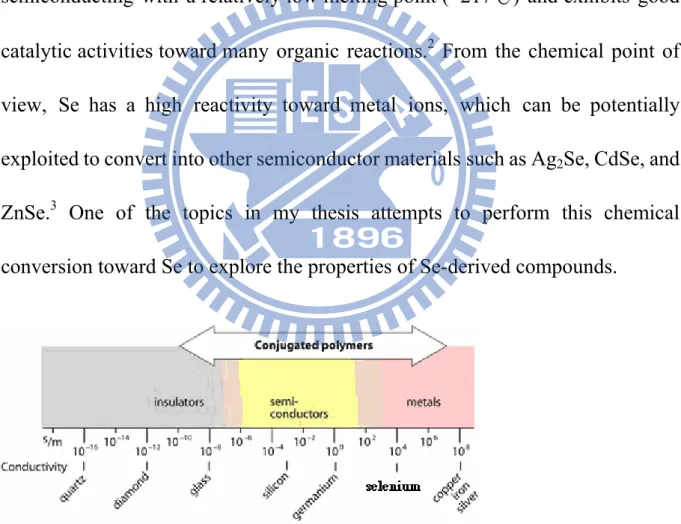
The most representative system for the growth of 1-D Se nanocrystals was first demonstrated by Xia et al. They succeed to obtain trigonal Se nanowires with uniform sizes through a simple “two-step” chemical reduction method1 and
a sonochemical approach.23 In the chemical reduction synthesis, selenious acid
and hydrazine were used as the precursor and reducing agent, respectively. The diameter of the as-synthesized Se nanowires can be well modulated by controlling the refluxing temperatures. As shown in Figure 1.2, the diameter of Se nanowires can be grown from 10 to 800 nm as increasing the refluxing temperatures from 90 to 130℃. Figure 1.3 displays the TEM images of high-quality Se nanowires which were synthesized by the sonochemical process.
Figure1.2 SEM images of Se nanowires with a mean diameter of 10 nm
obtained with a refluxing temperature of (A) 90oC, (B) 100 oC, (C) 110 oC, (D) 130 oC. The average diameter of Se nanowires was 10, 32, 100, 800 nm for (A), (B), (C), (D), respectively.1
Figure 1.3 Se nanowires synthesized through a sonochemical process: (A, B)
TEM images, (C) XRD pattern and a typical electron diffraction pattern (insert), (D) high-resolution TEM image obtained from the edge of an individual nanowire.23
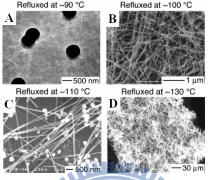
The “two-step” process means “seed and growth”, and it is a well-known system in the synthesis of Se nanowires. Xia et al illustrate a plausible mechanism as depicted in Figure 1.4.1 First, Se ion would be reduced by
appropriate reducing agent like hydrazine and uniform amorphous nanocrystals of Se were formed. Then, there were definite driving force which could make the amorphous Se nanocrystals re-construct to form nanowires.
Figure 1.4 Schematic illustration of the formation mechanism for Se nanowires
obtained in a “two-step" process.1
1.2.2 Recently Studies of Se 1-D Nanocrystals
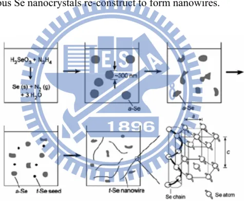
Even though the development of the synthetic system for Se nanocrystals has been nearly complete in the past decade, research regarding to 1-D Se nanorods is just popular in present. In the recent two years, Chen et al27 and
Mondal et al28 reported two organic-molecule-assisted synthetic systems that can
produce Se nanorods. These syntheses are different from those in previous studies, mainly coming from the utilization of shape-confining organic molecules such as L-cysteine. Figure 1.5 displays the TEM images of Se nanorods synthesized with the L-cysteine assisted hydrothermal process. By controlling the ultrasonic times, the diameter of Se nanorods could be effectively tuned. Figure 1.6 further shows the morphological evolution of Se nanorods with increasing hydrothermal reaction times.
There have been more and more studies about the soft-template-assisted synthetic system since these shape-confining soft templates could confine the growth of atoms to form various anisotropic nanocrystals. Through these recently reported studies, mechanism of Se nanorods formation get much more understood, but there still are lots of issues needed to be solved such as the wide size-distribution and non-uniformity of products and complicated experiment
setups. In this thesis, we try to solve these issues by carefully controlling the reaction conditions in a simple soft-template synthetic system.
Figure 1.5 TEM images of Se nanorods obtained with an ultrasonic time of (A)
14 min and (B) 20 min. Their corresponding HRTEM images were shown in (C) and (D).27
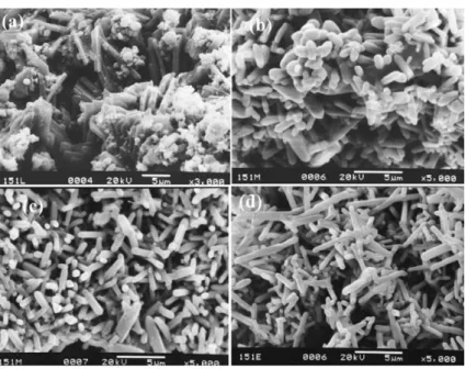
Figure 1.6 SEM images of Se nanorods prepared at the hydrothermal reaction
times of (a) 6 h, (b) 9 h, (c) 12 h, (d) 24 h.28
1.3 Soft-Template Synthesis
It has been well-known that specific organic compounds could be applied as the soft-template for the growth of inorganic nanomaterials. For the syntheses of Se nanocrystals in solution, polymers with long alkyl chains such as PVP and PVA are commonly used.17,18 Additionally, various polysaccharides, such as
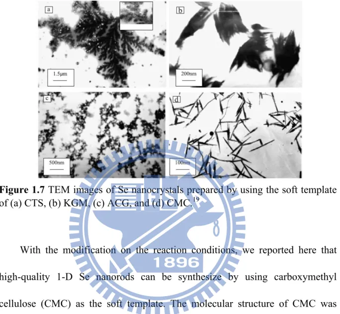
chitosan (CTS), konjac glucomannan (KGM), acacia gum (ACG) and carboxylmethyl cellulose (CMC), can be applied to obtain Se nanocrystals,19 but
the resulting morphologies were unfortunately not uniform. Figure 1.7 shows the TEM images of Se nanocrystals synthesized by using the above-mentioned polysaccharides as soft template.
Figure 1.7 TEM images of Se nanocrystals prepared by using the soft template
of (a) CTS, (b) KGM, (c) ACG, and (d) CMC.19
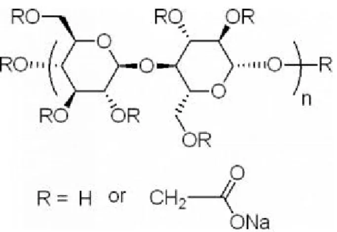
With the modification on the reaction conditions, we reported here that high-quality 1-D Se nanorods can be synthesize by using carboxymethyl cellulose (CMC) as the soft template. The molecular structure of CMC was shown in Figure 1.8, We studied in details the effect of reaction conditions on the morphologies of the resulting Se nanocrystals. A plausible reaction mechanism was also proposed to interpret the formation of 1-D Se nanorods in the presence of CMC.
Figure 1.8 Molecular Structure of CMC (carboxymethyl cellulose).
1.4 Cation-Exchange Reaction
Presently, an improved in-situ template method involving a cation-exchange reaction is demonstrated as an efficient way to “duplicate” nanostructures without altering the morphology.14,15 Large difference in the solubility product (Ksp) is a
key factor toward direct replacement between two kinds of cations. Nanocrystals can spontaneously be converted into another much stable one with smaller Ksp. For example, several cations including Cu+, Ag+, Sb3+, and Bi3+have been used to
replace Zn2+in ZnS nanotubes to produce the corresponding sulfides with the
preservation of the tubular shape.16
This approach opens up a new access to design and prepare nanostructures that is difficult to achieve through other general methods. Based on the concept introduced above, we performed the cation-exchange approach on Ag2Se
nanorods which were fabricated through the direct introduction of Ag+ into the
as-synthesized Se nanorods. The result showed that a series of selenides including ZnSe and CdSe can be obtained with the preservation of rod shapes.
1.4.1 Studies of Cation-Exchange Reaction
In order to extend the application of Se nanorods, we tried to exploit the high chemical activity of Se to transform Se into other semiconductor. The realization of cation-exchange seemed relevant to this concept, so we took a
survey of this method. In 2004, Alivisatos et al first published a research about the cation-exchange reaction for nanocrystals in Science, and they found some interesting phenomena about the reversible transformation between CdSe and Ag2Se nanocrystals.14 CdSe could be transformed into Ag2Se easily by the
addition of Ag+ due to thermodynamically favorable regime. Note that the
reverse transformation (i.e. from Ag2Se to CdSe) was thermodynamically
forbidden. Such conversion however can be achieved through a kinetically controlled approach, in which a large amount of Cd2+ and the reaction initiator
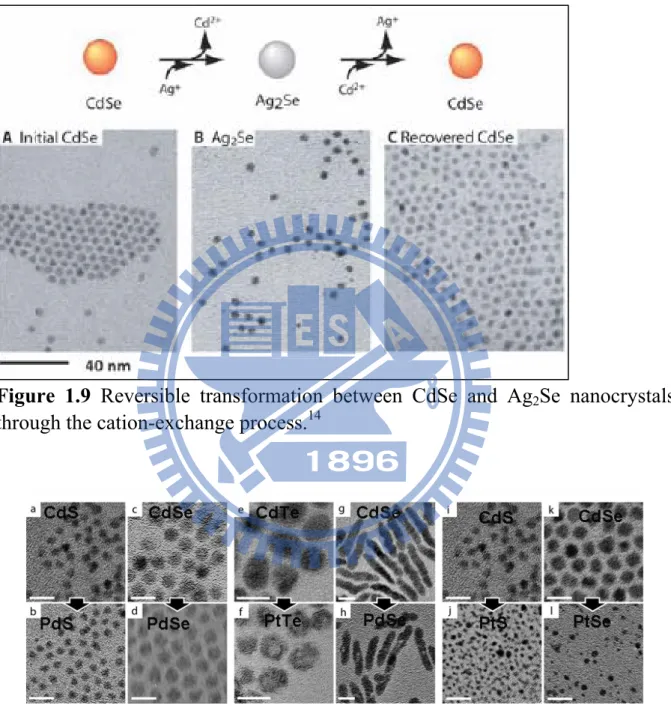
(TBP, tri-butyl phosphate) were necessarily added in the growth. As shown in Figure 1.9, the shape and dimension of nanocrystals could be reversibly maintained at suitable reaction conditions. Besides the result reported by Alivisatos, Wark et al succeed to synthesize various sulfides and selenides nanocrystals through the cation-exchange reaction.29 Figure 1.10 displays the
variety of sulfides and selenides nanocrystals obtained in the specific cation- exchange process. Note that even the rod-shape can be preserved for nanocrystals after the ion exchange reaction. The concept of cation-exchange reaction is applicable in our system because Se nanorods can be readily transformed into Ag2Se by adding Ag+. We could then perform cation-exchange
reaction upon the as-obtained Ag2Se nanorods to fabricate other selenides
nanorods.
Figure 1.9 Reversible transformation between CdSe and Ag2Se nanocrystals
through the cation-exchange process.14
Figure 1.10 TEM images of various sulfides and selenides nanocrystals
obtained by cation-exchange reaction.29
Chapter 2. Experimental Section
2.1 Chemicals
All chemicals used were analytic grade reagents and used without further purification.
1. Selenium(IV) oxide (SeO2), 98%, Aldrich
2. Sodium borohydride (NaBH4), 96%, Fluka
3. Sodium hydroxide (NaOH), 98%, Mallinckrodt
4. Carboxymethyl cellulose (CMC), Sodium salt, 98%, Sigma 5. Silver nitrate (AgNO3), 99.9%, J.T.Baker
6. Zinc nitratre hexahydrate (Zn(NO3)2), 98%, Riedel-deHaën
7. tri-Butyl phosphate (TBP), 96%, Kanko Chemical 8. Cadmium nitrate tetrahydrate (Cd(NO3)2), 98%, Fluka
9. Polyvinylpyrrolidone (PVP), MW=10000, 99%, Sigma Aldrich
2.2 Instruments
1. Field-Emission Scanning Electron Microscope (FESEM):Jeol, JSM-6500F, operated at 15 kV
2. Transmission Electron Microscope (TEM):Philips Tecnai, F20 G2, operated at 200kV
3. UV-Visible Spectrophotometer:Hitachi, U-3900H
4. X-ray photoelectron spectroscope (XPS):VG Scientific, Microlab 350 5. X-Ray Diffraction (XRD):MAC Science, MXP18, operated at 40kV and
30mA
2.3 Preparation of Se Nanorods
First, 4.0wt %CMC solution was prepared and stored at room temperature. 0.0821g SeO2 (0.74 mole) was then dissolved in 9mL CMC solution, and 1M
NaOH solution of 1mL was added into it with vigorous stirring at 25℃ until the solution turned transparent. Subsequently, NaBH4 solution of 0.79 mole (0.030g
NaBH4 in 1mL deionized water) was added dropwise with a rate of about
0.2μL/sec into the selenious solution. The color of the solution changed quickly from transparent to brick red. After the stand for 4 hours at 25℃, the color of solution would change from brick red to brown. The product (Se nanorods) was collected by centrifugation at 10000 rpm for 10 min and washed with distilled water and ethanol to remove remaining ions and impurities. The washed product was then dried and stored at 60℃ in vacuum for later characterization and use.
2.4 Preparation of Ag
2Se, CdSe, ZnSe Nanorods
Ag2Se nanorods were obtained through the direct introduction of Ag+ into
Se nanorods at room temperature. CdSe and ZnSe nanorods were then produced using the cation-exchange approach from the as-obtained Ag2Se nanorods. For
the preparation of Ag2Se nanorods, 0.0395g Se NRs (5×10⁻⁴ mole) were first
re-dispersed in 10mL of 5% PVP solution. AgNO3 solution of 10mL (0.17g
AgNO3, 1×10⁻³ mole) was then added dropwise into Se nanorod solution. The
solution was stirred for reaction at 25℃ in water bath. The product was obtained after the color of the solution turned to black. The product (Ag2Se
nanorods) was collected by centrifugation at 8000 rpm for 10 min and washed with distilled water and ethanol for several times. The washed product was then dried and stored at 60℃ in vacuum for later characterization and use.
For the synthesis of CdSe nanorods, 0.147g Ag2Se nanorods (5×10⁻⁴ mole)
were re-dispersed in 10mL of 5% PVP solution and put into round-bottom flask with vigorous stirring at 80℃. Cd(NO3)2 of 2.364 g (1×10⁻² mole) was dissolved
in 20mL methanol. The above two solutions were then mixed to reach the thermal equilibrium at 80℃. 300μL TBP was injected into the above mixing solution to proceed with the cation-exchange reaction. After six hours of reaction, the solution turned dark-red and was cooled down naturally. As to the
fabrication of ZnSe nanorods, Zn(NO3)2 of 1.894g (1×10⁻² mole) was used as the
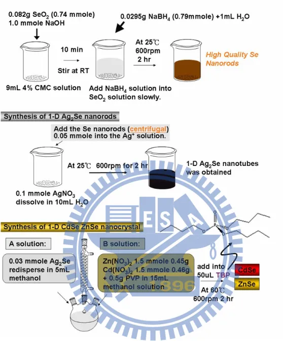
cation source, followed by the same procedure performed in the synthesis of CdSe nanorods. The product (CdSe and ZnSe nanorods) was collected by centrifugation at 8000 rpm for 10 min and washed with distilled water and ethanol for several times. The washed product was then dried and stored at 60℃ in vacuum for later characterization. A schematic illustration of the whole experimental procedures in this work was depicted in Figure 2.1.
Figure 2.1 Schematic illustration of the experimental procedure.
2.5 Preparation of Se Nanorod Film for Electrical Measurement
Nanorod film, well adhered to Si substrates, was prepared by dripping nanorod suspensions of sufficient amount onto Si wafers, followed by a heat treatment to remove the solvent.
2.6 Photocatalytic Activity Study
Photodecomposition of methylene blue (MB) was monitored to test the photocatalytic activity of the as-prepared Se nanorods. Irradiation was provided by a UV lamp (8W) with a wavelength of 275 nm. The concentration of MB in the presence of Se nanorods under illumination was determined by the absorption spectra on the basis of Beer’s Law.
2.7 Characterizations
The morphology and dimensions of the products were examined with a field-emission scanning electron microscope (FESEM, Jeol, JSM-6500F). The crystallographic structure of the samples was investigated with X-ray diffraction (XRD, MAC Science, MXP18) and a high-resolution TEM (Philips Tecnai, F20 G2) operated at 200 kV. The compositional information was obtained with an energy dispersive spectrometer (EDS), an accessory of the TEM (F20 G2), and
X-ray photoelectron spectroscope (XPS, VG Scientific, Microlab 350). UV-Visible absorption spectra were obtained using a Hitachi U-3900H at 25oC
under ambient atmosphere. Electrical measurement for the Se nanorod film was conducted under white-light (Halogen lamp, 150W) and UV illumination (UV lamp, 30mW) via a Keithley 236 semiconductor parameter analyzer by contacting the film surface with two measuring microprobes.
Chapter 3. Results and Discussion
3.1 High-Quality Se Nanorods
Reduction of SeO2 by NaBH4 in the presence of CMC produced nanorods
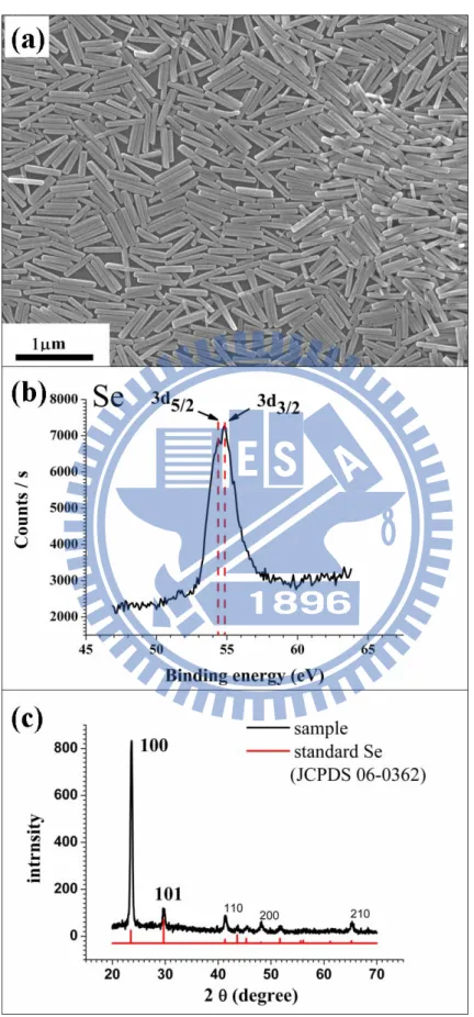
with considerably uniform dimensions. From the SEM image shown in Figure 3.1(a), the dimension of the as-prepared nanorods was 45±3 nm in diameter and 500±28 nm in length. The compositional information of nanorods was then studied with XPS and XRD. Figure 3.1(b) shows XPS spectrum of the as-synthesized nanorods. Note that the binding energies obtained in the XPS analysis were corrected for specimen charging by referencing the C1s to 284.60 eV. In Figure 3.1(b), the binding energies observed at 54.4 and 54.8 eV correspond well to Se3d5/2 and Se3d3/2 peaks of elemental Se, respectively,20
implying that nanorods were made of Se. The corresponding XRD pattern in Figure 3.1(c) confirms the formation of elemental Se. All the diffraction peaks in this spectrum can be indexed as the hexagonal phase of Se by referring to the reference (JCPDS, No.06-0362). As a result of these two surveys, it was confirmed that we succeed in synthesizing high-quality Se nanorods with considerably uniform dimensions.
Figure 3.1. (a) SEM image, (b) XPS spectrum and (c) XRD pattern of the
as-synthesized Se nanorods.
To obtain more details about structures of Se nanorods, HRTEM and SAED were exploited and the result was shown in Figure 3.2. From the HRTEM image of Figure 3.2(b), a growth direction of [001] could be observed for the as-synthesized Se nanorods. In addition, the dot-pattern of SAED in Figure 3.2(c) revealed the single-crystallinity of Se nanorods. The growth direction of [001] for Se nanorods explained why (100) peak was the most intense among the other crystallographic planes in the XRD survey. Because the direction of X-ray was basically parallel to the longitudinal direction of nanorods (i.e. the [001] direction), a direction of [100] which was perpendicular to [001] would possess the highest probability during the diffraction of X-ray.
Figure 3.2 (a) TEM image, (b) HRTEM and (c) SAED images of the
as-synthesized Se nanorods.
3.2 Formation Mechanism of Se Nanorods
The growth mechanism of 1-D Se nanocrystals has been extensively
investigated in many solution-based approaches. In general, there are three steps involved in the solution-phase growth of 1-D Se nancrystals. At first, the precursor of Se was reduced by suitable reducing agent to form amorphous Se (a-Se) particles of hundreds nm in sizes. Secondly, trigonal Se nanocrystals (t-Se) were accompanied to generate by providing definite driving force for system, such as sonication operation,21 variation of temperature or exertion of high
pressure.22 Finally, Ostwald ripening took place in solution to re-dissolve a-Se,
leading to the further growth of 1-D Se nanocrystals.23 The re-dissolution of a-Se
was probably due to its higher surface energy than t-Se. The above mechanism however didn’t account for the formation of Se nanorods in our experiment because we didn’t observe the generation of a-Se and no extra driving force was provided in the system. To interpret the growth of the as-synthesized Se nanorods, experiments with various reaction times were performed and the resulting morphologies were compared in Figure 3.3. At the beginning of reaction, Se particles of 40-60 nm in sizes were produced, followed by a particle-to-particle aggregation. A branch was then pulled out of individual particle-to-particle
blocks, resulting in the formation of quarsi-1-D nanostructures. As the reaction proceeded, 1-D nanorods shaped up with considerably uniform dimensions.
Figure 3.3. SEM images of Se nanorods obtained with different reaction times:
(a) 5 min, (b) 10 min, (c) 20 min, (d) 40 min, (e) 60 min, (f) 80 min, (g) 100 min, (h) 2hr, and (i) 4hr.
A schematic illustration of the formation mechanism for the current Se nanorods was proposed and shown in Figure 3.4. At the beginning of reaction, Se particles with 40 nm in sizes were generated through the reduction of SeO2 by
NaBH4. The polysaccharide of CMC added in the growth solution may surround
Se particles, forming the quasi-1-D channels for the later crystal growth. After this stage, Se started to nucleate and grow at the surfaces of the first-formed
particles, which can be inferred from the morphology observed at 40 min of reaction time. Due to the confinement of the quasi-1-D channels built by CMC molecules, anisotropic growth may start to dominate the growth of Se,
resulting in the formation of 1-D nanocrystals.
Figure 3.4 A schematic illustration of the formation mechanism for Se
nanorods.
The quasi-1-D channels formed by CMC molecules can be further verified with the Mark–Houwink equation which is usually applied to investigate the rheological structures of polymers. Here is the expression of Mark-Houwink equation: weight molecular average -Viscosity : M viscosity Limiting : ] [ constant Houwink – Mark : K KM ] [ parameter Houwink – Mark : : Equation Houwink – Mark η η α α =
By referring to the value of α, one is able to identify the rheological structures of the tested molecules. For most of the flexible polymers, the value of α is between 0.5 to 0.8. As to the semi-flexible polymers, α is found to be larger than 0.8. For
polymers with an absolute rigid rod-shape, the value of α is roughly 2.0.31 As
shown in Figure 3.5, the rod shape was clearly revealed for the polysaccharide molecule (tobacco mosaic virus) with the α value of 2.0.33 It was known that an
increase in α value was observed for CMC molecules with increasing concentration of NaOH.32 Thus, it’s reasonable to infer that the rheological
structure of CMC is also the absolute rigid rod. Although the exact structure of CMC molecules was not observed in solution, the rod-shaped rheological structures supported the soft-template concept in the growth of Se nanorods in this work.
Figure 3.5 (A) Rheological structure of polysaccharides when α > 2.0. (B)
TEM image of tobacco mosaic virus particles.31,33
3.3 Morphological Control of Se Nanorods
3.3.1 Effect of pH value
It should be noted that we failed to obtain nanorods of Se in the CMC-assisted chemical reduction system without the addition of NaOH. It is therefore worthy to investigate the role of NaOH played in the growth of Se nanorods in this system. It was found that by changing the amount of NaOH we added, the dimension of the resulting Se nanorods can be effectively tuned. As increasing the amount of NaOH from 0.6 to 1.2 mmol, the length of Se nanorods increased evidently, accompanied by a slight growth in diameter. As shown in Figure 3.6, Se nanorods with 200 nm in length and 40 nm in diameter can be obtained when 0.6 mmole NaOH was added. When the amount of NaOH was raised to 0.8 mmol, the mean length of Se nanorods increased to 350 nm. With the addition of 1.0 mmole NaOH, we could obtain Se nanorods with longer length of 450 nm. A further increase of NaOH to 1.2 mmol produced Se nanorods with 80 nm in diameter and 884 nm in length. A more detailed relation between the amount of NaOH added and the length of Se nanorods was depicted in Figure 3.7.
Figure 3.6 TEM images of Se nanorods obtained with various amounts of
NaOH added: (a) 0.6 mmole, (b) 0.8 mmole, (c) 1.0 mmole, (d) 1.2 mmole.
Figure 3.7 Relation between the amount of NaOH added and the length of Se
nanorods.
When the amount of NaOH increased from 0.1 mmole to 1.2 mmole, the length of Se nanorods increased gradually. But this tendency was terminated when NaOH of more than 1.2 mmol was added. This phenomenon could be explained by three concepts. First, the addition of NaOH would alter the pH value of CMC solution, which is determinant to the viscosity of CMC.24 CMC solution
is stable with a constant viscosity at the pH value of 2 ~10.24 An amount of NaOH
of more than 1.2mmole resulted in a pH value over 10 of the solution, which may significantly reduce the viscosity of CMC and thus losing its ability to stabilize the growth of Se. Consequently, the lengths of the Se nanorods get shortened when more than 1.2 mmol of NaOH was added. Secondly, the pH value would affect the reducing ability of NaBH4.25 The higher the pH value gets, the less
reducing ability NaBH4 shows, leading to the slow growth of Se and thus shorter
nanorods. Lastly, the solubility of Se4+ ion may also play an important role since it
is related to the pH value, too. The solubility of Se4+ gets higher with increasing
pH value.22 It explained why the length of Se nanorods increased with increasing
amount of NaOH added since there are increasing amount of Se4+ ions that can be
readily consumed.
Because Se crystal possesses the direct bandgap energy of 1.95 eV and the indirect bandgap energy of 1.85 eV, its optical property would be revealed by
measuring the UV-Vis spectrum. Figure 3.8 shows the UV-Vis spectra of Se nanorods with different lengths. From these spectra, we could observe the direct bandgap absorption at about 636nm (1.95eV). Besides, the absorbance at around 600nm increased with increasing length, possibly due to the interaction among the inside-chain atoms of Se nanorods in the [001] direction.30
Figure 3.8 UV-Vis spectra of Se nanorods with different lengths.
3.3.2 Effect of Reaction Temperature
From the viewpoint of growth kinetics, higher reaction temperature caused the higher reaction rate, which could probably vary the dimensions of the resulting nanorods. It is thus expected that Se nanorods became longer in length and larger in diameter as increasing the reaction temperature. From the SEM result of Figure 3.9, we concluded undoubtedly that Se nanorods with larger dimensions in both diameter and length can be produced as the reaction temperature is increased.
Figure 3.9. SEM images of Se nanorods obtained at the reaction temperatures of
(A) 25℃, (B) 50 ,℃ (C) 75℃ and (D) 100℃.
3.3.3 Effect of CMC Concentration
We also tried to change the concentration of CMC solution (wt 0%, 2%, 4%, 6%, and 8%) to see if Se nanorods with different dimensions can be obtained. As shown in Figure 3.10, a CMC solution of 4% was found to be the optimal recipe for the growth of Se nanorods. Experiments with CMC of lower or higher concentrations produced Se nanocrystals with irregular morphologies.
Figure 3.10. SEM images of Se nanocrystals obtained with a CMC
concentration of (a) 0%, (b) 2%, (c) 4%, (d) 6% and (e) 8%.
3.3.4 Effect of NaBH
4Concentration
Experiments with different molar ratio of reducing agent (NaBH4) to SeO2
were conducted to study its influence on the morphology of product. As shown in Figure 3.11, a molar ratio of 0.5 produced Se nanoparticles instead of nanorods because there was not enough amount of reducing agent to reduce Se2+
ion. As the ratio was raised to 1, nanorods of Se with uniform dimensions resulted. Further increase in the ratio of NaBH4 to SeO2 produced rod-like
nanocrystals of Se with irregular dimensions.
Figure 3.11. SEM images of Se nanocrystals obtained with the molar ratio
(NaBH4 to SeO2) of (a) 0.5, (b) 1.0 and (c) 2.0.
3.3.5 Effect of Type of Reducing Agent
In this work, other reducing agents (hydrazine and ascorbic acid) that are commonly used in the synthesis of inorganic nanocrystals were also utilized to synthesize Se nanocrystals. As shown in Figure 3.12, nanorods of Se with a much shorter length can be fabricated by using hydrazine as the reducing agent. On the other hand, Se particles of irregular shapes were produced when ascorbic acid was utilized.
Figure 3.12. SEM images of Se nanocrystals obtained by using the reducing
agents of (a) NaBH4, (b) hydrazine and (c) ascorbic acid.
3.4 Direct Introduction of Ag
+into Se Nanorods
It was reported that silver selenide (Ag2Se) can be formed through a direct
introduction of Ag+ into Se crystals at room temperature. The reaction involved
in this process can be shown as follows:3
+
+ + ⎯⎯→ + +
+6Ag 3H O 2Ag Se(s) Ag SeO (aq) 6H
3Se (s) (aq) 2 2 2 3
As shown in Figure 3.13(a), a 2:1 molar ratio of Ag+ to Se nanorods produced
Ag2Se nanocrystals with rod-shaped morphology. The corresponding EDS and
XRD analyses confirmed the composition of the resulting nanorods as Ag2Se.
Figure 3.13. (a) SEM image, (b) EDS analysis and (c) XRD pattern of Ag2Se
nanorods.
3.5 Cation-Exchange Reaction for Ag
2Se Nanorods
The cation-exchange reaction was carried out for the as-synthesized Ag2Se
nanorods to obtain CdSe and ZnSe nanocrystals. From the SEM result shown in Figure 3.14, the rod shape was found to preserve after the cation-exchange reaction. The EDS analysis indicated that nanorods of CdSe and ZnSe were successfully obtained by exchanging Ag+ of Ag2Se with Cd2+ and Zn2+,
respectively. Then, the UV-Vis spectra shown in Figure 3.15 would be exploited to observe the bandgap energy of the products.
Figure 3.14. (a) SEM image and (b) EDS analysis of CdSe nanorods. (c), (d) are
for ZnSe nanorods.
Figure 3.15 UV-Vis spectra of Se, Ag2Se, CdSe and ZnSe nanorods. The inset
arrows indicated the observed bandgap energies.
3.7 Photoconductivity of Se nanorods
Figure 3.16 shows the typical I-V curves of Se nanorod film under different illumination conditions. It was found that visible light could stimulate photocurrents inside Se nanorods. A much more drastic enhancement of about an order of magnitude in photocurrents was observed for Se nanorods under the UV illumination. The above result indicated that the as-prepared Se nanorods can be integrated as the photoconducting devices. To demonstrate this potential application, we tested the reversible switching of nanorod film between low and high conductance states when the UV light was turn on and off. The
characteristics of the photoconductive Se nanorods suggest that they are good candidates for optoelectronic switches, with dark insulating states as “off” and the light-excited conducting state as “on”.
Figure 3.16. (a) I-V curves of Se nanorod film under different illumination
conditions. (b) Reversible switching of Se nanorod films between low and high conductance states when the UV light was turn on and off. The bias on the film is 10V.
3.8 Photocatalytic Activity of Se Nanorods
A great enhancement in the photocurrents was observed for Se nanorods upon light illumination, implying that photo-induced charge carriers of a
considerable amount can be produced therein. One effective way to utilize these photogenerated charge carriers in Se nanorods is to perform the photocatalytic reaction. We chose MB as a representative organic dye for the photocatalysis test. Figure 3.17(a) shows the time-dependent UV-Vis absorption spectra of MB solution during the photodegradation in the presence of Se nanorods. MB solution exhibits two characteristic absorption bands at around 610 and 660 nm. The absorbance of these two bands got less intense during the course of photocatalysis. The decolorization was completed at 30 min of irradiation for the Se nanorods. The result for Degussa P25 TiO2 was included in Figure 3.17(b) for
comparison, which shows a lower efficiency of MB degradation. In Figure 3.17(c), the decolorization comparison of MB over irradiation time revealed that Se nanorods showed more effective phtocatalytic activity than P25. The result indicated that the as-synthesized Se nanorods possessed high photocatalytic activity for MB degradation under UV light.
Figure 3.17. Time-dependent absorption spectra of the MB solution in the
presence of (a) Se nanorods and (b) P25. (c) Comparison of MB degradation under UV illumination between Se nanorods and P25.
Chapter 4. Conclusion
In this thesis, high-quality Se nanorods have been successfully synthesized
using the CMC-assisted chemical reduction approach. The growth mechanism for Se nanorods was systematically studied and discussed. We demonstrated that CMC could form the quasi-1-D channels surrounding the Se nanocrystals, enabling the occurrence of anisotropic growth of Se to form nanorods. Control over the resulting morphology of Se can be achieved through carefully modulating the relevant reaction conditions. Through the direct incorporation of Ag+ into Se, Ag2Se nanorods could be readily obtained. In addition,
cation-exchange reaction was performed on the as-synthesized nanorods of
Ag2Se, resulting in the formation of CdSe and ZnSe nanorods. The
photoconductive properties of the as-synthesized Se nanorods were characterized, demonstrating their potential applications in optoelectronic switching devices. Furthermore, the as-obtained Se nanorods showed considerably high photocatalytic activity for MB degradation under UV light illumination, implying that they could be a good photocatalyst for many species.
References
1. Gates, B.; Mayers, B.; Cattle, B.; Xia, Y. N. Adv. Funct. Mater. 2002, 12, 219. 2. Mort, J. J. Appl. Phys. 1968, 39, 3543–3549.
3. Gates, B.; Wu, Y. Y.; Yin, Y. D.; Yang, P. D.; Xia, Y. N. J. Am. Chem. Soc. 2001, 123, 11500.
4. Duan, X.; Huang, Y.; Cui, Y.; Wang, J.; Lieber, C. M. Nature (London) 2001, 409, 66. 5. Jiang, Z. Y.; Xie, Z. X.; Xie, S. Y.; Zhang, X. H.; Huang, R. B.; Zheng, L. S. Chem. Phys.
Lett. 2003, 368, 425.
6 .Zhang, H.; Yang, D.; Ji, Y. J.; Ma, X. Y.; Xu, J.; Que, D. L. J. Phys. Chem. B 2004, 108, 1179.
7. Ren, L.; Zhang, H. Z.; Tan, P. H.; Chen, Y. F.; Zhang, Z. S.; Chang, Y. Q.; Xu, J.; Yang, F. H.; Yu, D. P. J. Phys. Chem. B 2004, 108,4627.
8. Zhang, S. Y.; Liu, Y.; Ma, X.; Chen, H. Y. J. Phys. Chem. B 2006,110, 9041.
9. Zhang, B.; Dai, W.; Ye, X. C.; Zuo, F.; Xie, Y. Angew. Chem. Int. Ed. 2006, 45, 2571. 10. Li, X. M.; Li, Y.; Li, S. Q.; Zhou, W. W.; Chu, H. B.; Chen, W.; Li, I.; Tang, Z. K. Cryst.
Growth Des. 2005, 5, 911.
11. Lu, Q. Y.; Gao, F.; Komarneni. S. Chem. Mater. 2006, 18, 159.
12. Ma, Y. R.; Qi, L. M.; Ma, J. M.; Cheng, H. M. Adv. Mater. 2004, 16, 1023.
13. Mayers, B.; Jiang, X.; Sunderland, D.; Cattle, B.; Xia Y. J. Am. Chem. Soc. 2003, 125, 13364
14. Son, D. H.; Hughes, S.M; Yin. Y.; Alivisatos, A.P., Science, 2004, 306, 1009 15. Zhu, W.; Wang, W.; Shi, J., J. Phys. Chem. B 2006, 110, 9785-9790
16. Dloczik, L.; Ko¨nenkamp, R. Nano Lett. 2003, 3, 651.
17. Song, J. M.; Zhu, J. H.; Yu, S. H., J. Phys. Chem. B 2006, 110, 23790-23795
18. Xiong, S. L.; Xi, B. J.; Wang, W. Z.; Wang, C. M.; Fei, L. F.; Zhou, H. Y.; Qian, Y. T.,
45
Cryst. Growth Des. 2006, 6, 1711
19. Zhang, S. Y.; Zhang, J.; Wang, H. Y.; Chen, H. Y. Mater. Lett. 2004, 58, 2590–2594
20. Panakkattu K. Babu et al. J. Am. Chem. Soc. 2007, 129, 15140-15141
21. Zhu, W.; Wang, W. Z.; Xu, H. L.; Zhou, L.; Zhang, L. S.; Shi, J. L. J. Cryst. Growth, 2006,
295, 69–74
22. Xi, G.; Xiong, K.; Zhao, Q.; Zhang, R.; Zhang, H.; Qian, Y. Cryst. Growth Des. 2006, 6, 577
23. Gates, B.; Mayers, B.; Grossman, A.; Xia, Y. Adv. Mater. 2002, 14,1749 24. Eremeeva, T. E.; Bykova, T.O. Carbohydr. Polym. 1998, 36, 319–326 25. Chatain, V.et al. J. Hazard. Mater. 2005, 122, 119–128
26. Lapasin R.; Pricl S. Rheology of Industrial Polysaccharides 1995, 250-494
27. Chen, Z. X.; Shen, Y. H.; Xie, A. J.; Zhu, J. M.; Wu, Z. F.; Huang, F. Z. Cryst. Growth
Des. 2009, 9, 1327
28. Kamalesh, M.; Poulomi, R.; Suneel, K. S.Cryst. Growth Des. 2008, 8, 1580
29. Wark, S. E.; Hsia, C. H.; Soon, D. H. J. Am. Chem. Soc. 2008, 130, 9550 30. Joannopoulos, J. D.; Schlüter, M.; Cohen, M. L. Phys. Rev. B 1974, 11, 2186 31. Lapasin R.; Pricl S. Rheology of Industrial Polysaccharides 1995, 250-494 32. Eremeeva, T. E.; Bykova, T. O. Carbohydrate Polymers 1998, 36, 319–326 33. Stryer, L. “Biochemistry” 3rd edition, 1988, W.H. Freeman & Company.