Effect of gold coating on local oxidation using an atomic force microscope
J. S. Hwang,a兲Z. Y. You, S. Y. Lin, and Z. S. Hu
Institute of Optoelectronic Sciences, National Taiwan Ocean University, Keelung, Taiwan C. T. Wu and C. W. Chen
Department of Material Science and Engineering, National Taiwan University, Taipei, Taiwan K. H. Chen
Institute of Atomic and Molecular Sciences, Academia Sinica, Taipei, Taiwan
共Received 20 December 2004; accepted 9 March 2005; published online 11 April 2005兲
A simple method to enhance atomic force microscopy local oxidation by coating the substrate with a thin layer of gold is reported. The effect of gold coating is demonstrated experimentally by atomic force microscopy oxidation at various thicknesses of gold on Si and InP. Oxide heights reaching 30 nm are easily achieved on silicon at rates 10 times greater than traditional methods. The gold layer is assumed to increase conductance and current during oxidation, thereby reducing decline in growth rates caused by the increasing resistance of the growing oxide layer itself. Improvement in growth rate and height increases with increasing gold thickness up to a maximum height, but beyond that thickness the heights and rates decrease because the gold layer itself becomes a barrier to the migration of oxyions. The presented method is demonstrated to improve the oxidation rate and height on normal and highly resistive substrates, with lower requirements for applied voltage during oxidation. © 2005 American Institute of Physics.关DOI: 10.1063/1.1901804兴
Local oxidation using an atomic force microscope 共AFM兲, or AFM nano-oxidation, is a promising scanning-probe-based lithography method suitable for fabrication of nanometer scale structures and devices.1–8 The tremendous electric field built by the applied voltage and the automati-cally formed “water bridge” 共water meniscus兲 between the AFM conducting tip and the substrate in an ambient environ-ment are capable of inducing anodic oxidation on the sub-strate and forming nanoscale oxide patterns. The electric field, reaching the order of 109V / m, has been applied to the local oxidation of silicon, GaAs,9 silicon nitride,5,10 silicon carbide,11metals,12–15and even oxides,7,16–18including high-temperature superconductors. Fabrication of nanoelectronic devices such as transistors,1,7,19–21 single electron memory,4 Josephson junctions, and superconducting quantum interfer-ence devices6,18 共SQUID兲 with AFM nano-oxidation has been demonstrated.
For potential mass production of nanodevices, it is es-sential to develop nano-oxidation techniques with high growth rates, which will enable not only increased final ox-ide heights but also easy oxidation of other than highly doped substrates. Tello et al.22have reported on this issue by replacing the water bridge with alcohol, thereby attaining oxide heights exceeding 20 nm on silicon with a growth rate 4–5 times higher than those obtained under the same condi-tions in water. Simpler than Tello’s alcohol bridge, our present study continues the use of the traditional water bridge in an ambient environment. The proposed method can produce oxides reaching a few tens of nanometers in height with an estimated growth rate 10 times greater than tradi-tional water-based methods under identical conditions on semiconductor substrates including Si and InP at low applied voltage, without requiring a highly doped substrate. The nano-oxidation of semi-insulating InP is reported, in contrast
to the tip-induced oxidation observed during carrier profiling using scanning spreading resistance microscopy23 on nor-mally doped InP substrates.
Our method requires a simple coating of the substrate with gold, which can presumably be replaced with other noble metals. Figure 1 shows the schematic diagram of the method. It is known that during the process of conventional AFM oxidation with constant applied voltage, as the insulat-ing oxide is forminsulat-ing, the total resistance of the circuit in-creases rapidly with simultaneous decrease of the current flow. The current flow helps drive oxyanions2,24such as OH− and O2−in the water bridge through the forming oxide
bar-rier to the SiO2/ Si interface, inducing further oxidation, but both current reduction and the diffusion barrier of the formed oxide limit growth rate and the final growth height of the silicon oxide. Therefore, coating the substrate with a thin conductive layer such as gold reduces the current decay that results from increasing oxide resistance. Likewise, the in-creased surface conductivity from the coating also helps en-large initial current flow. However, it should be noted that the conductive layer itself can become a diffusion barrier at larger thicknesses, which implies the existence of an optimal
a兲Author to whom correspondence should be addressed; electronic mail:
[email protected] FIG. 1. Schematic diagram of gold coating enhanced AFM local oxidation. APPLIED PHYSICS LETTERS 86, 161901共2005兲
0003-6951/2005/86共16兲/161901/3/$22.50 86, 161901-1 © 2005 American Institute of Physics
conductive layer thickness for enhancement of local oxida-tion.
We have demonstrated the effect on nano-oxidation of gold coating using a NTMDT P47H AFM. Surface-cleaned
p-type 共100兲 silicon 共with a resistivity of 4.1 ⍀ cm兲 and
semi-insulating InP 共100兲 共AXT, Inc., with a resistivity of 5.5⫻106⍀ cm and a carrier concentration of 1.1 ⫻1013cm−3, evaluated under a standard Hall effect
measure-ment system兲 were coated with gold layers of various thick-nesses using a sputter coater共Emitech K575X兲 before local oxidation. Local oxidation was performed using the tapping mode by applying a negative pulse voltage of 84 ms within 1 Hz duration on a conductive Pt-coated silicon tip scanning at the speed of 3000 Å / s under a humidity of 70%. A JEOL JEM-2000FX transmission electron microscope共TEM兲 was used to observe the grown oxide.
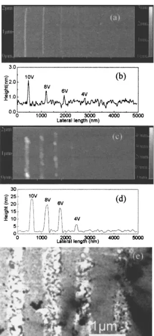
Figures 2共a兲–2共d兲 show typical AFM images and oxide heights of oxidation performed on a pure silicon substrate
关Figs. 2共a兲 and 2共b兲兴 and a Au-coated silicon substrate 关Figs. 2共c兲 and 2共d兲兴 at various applied voltages. Our results show the oxide height on Au-coated silicon is much greater than that grown on a pure silicon substrate, but with irregular height along the oxidative lines. After examination by AFM, the irregular height seems due to peeled portions关an unusu-ally bright spot in Fig. 2共c兲兴 of the gold film extruded by oxide grown beneath the metal film. This interpretation was reinforced by the existence of a trench on the substrate after the oxide line was etched away in HF and by a TEM planar view micrograph shown in Fig. 2共e兲, which further evi-denced the oxide grown beneath the gold layer. Note that the oxide lines in the TEM micrograph, whose width 共⬃500 nm兲 is apparently larger than that in Fig. 2共d兲, was intentionally grown at high humidity共⬃90%兲 to make pos-sible the TEM sample preparation under the optical micro-scope. The dependence of oxide height on applied voltage for the AFM images of Figs. 2共a兲 and 2共c兲 can be seen re-spectively in Figs. 2共b兲 and 2共d兲, both of which demonstrate the typical decay in height at lower voltages. Nevertheless, the voltage required to attain the same oxide height for the gold-coated sample is apparently much lower than that needed for pure silicon. Since oxidation of the two samples was performed under identical conditions and identical oxi-dation times, a comparison of Figs. 2共b兲 and 2共d兲 shows an estimated growth rate on the Au-coated silicon substrate that is at least 10 times greater than without Au coating.
For further clarification of the effect of gold coating, local oxidation on silicon substrates coated with different thicknesses of the gold layer were conducted. The relations of the average height and width of the oxide lines to the FIG. 3. AFM oxidative共a兲 height and 共b兲 width dependence on gold thick-ness under two applied voltages共8 and 10 V兲; the solid lines connecting data points are only for visual guides.
FIG. 2.共a兲–共d兲 Typical AFM images and oxide height of local oxidation on 共a兲, 共b兲 pure silicon substrate and 共c兲, 共d兲 silicon substrate with a 29-nm gold coating, at different applied voltages.共e兲 TEM planar view micrograph of oxide lines共brighter part兲 grown by AFM oxidation on silicon substrate with a 22-nm gold coating at an applied voltage of 10 V.
161901-2 Hwanget al. Appl. Phys. Lett. 86, 161901共2005兲
thickness of the gold layer are shown, respectively, in Figs. 3共a兲 and 3共b兲. Figure 3共a兲 shows that as the thickness of gold increases, the height and width of the oxide also increase, reaching a maximum at 22 nm of gold. As the thickness of the gold layer increased further, the vertical and lateral di-mensions of the grown oxide decreased. This behavior can be explained by the concepts discussed earlier in this letter 共Fig. 1兲, i.e., the thin gold layer during oxidation increases both conductance and current, which helps migration of oxy-ions to the silicon/SiO2 interface. However, when the gold layer becomes thicker than a certain value, it becomes a dif-fusion barrier and hampers migration of oxyions through the gold to the Si/ SiO2 interface. With regard to this, it is
be-lieved that microcracks or slits between gold grains in the sputtered gold layer constitute the main channels for oxyion migration. It should be mentioned that oxide growth stopped at a gold thickness beyond about 80 nm, which precludes the possibility of impurities in gold forming the oxide.
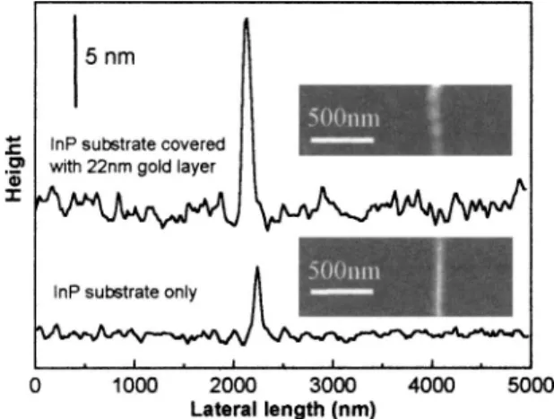
The effect of gold coating on oxidation was examined also on semi-insulating InP共100兲 substrates, with behavior similar to that found for silicon. Figure 4 compares the oxi-dation results of InP with and without gold coating, with AFM images shown in the insets. The height of the oxide lines with gold was about three times higher than without gold. We report here the AFM local oxidation on semi-insulating InP. Of note is the surprising ease of AFM oxida-tion on the pure semi-insulating InP substrate with a 5.5 ⫻106⍀ cm resistivity. Compared to the difficulty of local
oxidation of other high-resistivity substrates, the phenom-enon indicates a negative change of Gibb’s free energy dur-ing the reaction of the system at high applied voltage, show-ing the importance of chemical thermodynamics in the technique of AFM oxidation.
In conclusion, a simple method to enhance the AFM local oxidation by coating the substrate with a thin layer of gold has been reported. We have demonstrated the effect of
gold coating on the AFM local oxidation of various sub-strates including Si and InP. The grown oxidative heights can be increased to a few tens of nanometers with deposition of an appropriate thickness of gold on the surface of the silicon substrate for increased conductance and current. When the thickness of the gold is increased beyond a certain level, the grown oxidative height then decreases due to limited migra-tion of oxyions through the gold layer. The presented method, which assists oxidation on resistive substrates by improving efficiency as well as lowering the voltage required for oxidation, improves chances to realize AFM-based mass production of nanodevices.
The authors are grateful to financial support from the National Science Council共Grant No. NSC93-2112-M-001兲, Taiwan.
1
E. S. Snow, P. M. Campbell, F. A. Buot, D. Park, C. R. K. Marrian, and R. Magno, Appl. Phys. Lett. 72, 3071共1998兲.
2
R. Garcia, M. Calleja, and H. Rohrer, J. Appl. Phys. 86, 1898共1999兲.
3
E. B. Cooper, S. R. Manalis, H. Fang, H. Dai, K. Matsumoto, S. C. Minne, T. Hunt, and C. F. Quate, Appl. Phys. Lett. 75, 3566共1999兲.
4
K. Matsumoto, Y. Gotoh, T. Maeda, J. A. Dagata, and J. S. Harris, Appl. Phys. Lett. 76, 239共2000兲.
5
F. S. Chien, Y.-C. Chou, T. T. Chen, W.-F. Hsieh, T. S. Chao, and S. Gwo, J. Appl. Phys. 89, 2465共2001兲.
6
V. Bouchiat, M. Faucher, C. Thirion, W. Wernsdorfer, T. Fournier, and B. Pannetier, Appl. Phys. Lett. 79, 123共2001兲.
7
L. Pellegrino, I. Pallecchi, D. Marré, E. Bellingeri, and A. S. Siri, Appl. Phys. Lett. 81, 3849共2002兲.
8
A. Dorn, M. Sigrist, A. Fuhrer, T. Ihn, T. Heinzel, K. Ensslin, W. Wegsc-heider, and M. Bichler, Appl. Phys. Lett. 80, 252共2002兲.
9
Y. Okada, Y. Iuchi, M. Kawabe, and J. S. Harris, Jr., Appl. Phys. Lett. 88, 1136共2000兲.
10
F. S. S. Chien, J. W. Chang, S. W. Lin, Y. C. Chou, T. T. Chen, S. Gwo, T. S. Chao, and W. F. Hsieh, Appl. Phys. Lett. 76, 360共2000兲.
11
X. N. Xie, H. J. Chung, C. H. Sow, and A. T. S. Wee, Appl. Phys. Lett. 84, 4914共2004兲.
12
M. S. Hagedom, D. D. Litfin, G. M. Price, A. E. Gordon, and T. K. Higman, J. Vac. Sci. Technol. B 14, 4153共1996兲.
13
E. S. Snow and P. M. Campbell, Science 250, 1639共1995兲.
14
H. Sugimura, T. Uchida, N. Kitamura, and H. Masuhara, Appl. Phys. Lett. 63, 1288共1993兲.
15
K. Matsumoto, M. Ishii, K. Segawa, Y. Oka, B. J. Vartanian, and J. S. Harris, Appl. Phys. Lett. 68, 34共1996兲.
16
Y. R. Ma, C. Yu, Y. D. Yao, Y. Liou, and S. F. Lee, Phys. Rev. B 64, 195324共2001兲.
17
R. W. Li, T. Kanki, H. A. Tohyama, J. Zhang, H. Tanaka, A. Takagi, T. Matsumoto, and T. Kawai, J. Appl. Phys. 95, 7091共2004兲.
18
I. Song, B. M. Kim, and G. Park, Appl. Phys. Lett. 76, 601共2000兲.
19
P. M. Campbell, E. S. Snow, and P. J. McMarr, Appl. Phys. Lett. 66, 1388 共1995兲.
20
E. S. Snow, P. M. Campbell, R. W. Rendell, F. A. Buot, D. Park, C. R. K. Marrian, and R. Magno, Appl. Phys. Lett. 72, 3071共1998兲.
21
I. Pallecchi, L. Pellegrino, E. Bellingeri, A. S. Siri, and D. Marre, J. Appl. Phys. 95, 8079共2004兲.
22
M. Tello and R. Garcia, Appl. Phys. Lett. 83, 2339共2003兲.
23
M. W. Xu, P. Eyben, T. Hantschel, and W. Vandervorst, Jpn. J. Appl. Phys., Part 1 41, 1048共2002兲.
24
A. E. Gordon, R. T. Fayfield, D. D. Litfin, and T. K. Higman, J. Vac. Sci. Technol. B 13, 2805共1995兲.
FIG. 4. AFM oxide heights of local oxidation on共a兲 InP and 共b兲 InP with a 22-nm gold coating; insets show the corresponding AFM images.
161901-3 Hwanget al. Appl. Phys. Lett. 86, 161901共2005兲