Growth and Electrical Characteristics of Liquid-Phase
Deposited SiO
2on Ge
B.-C. Hsu,
*
W.-C. Hua, C.-R. Shie, K.-F. Chen, and C. W. Liu**
,z Department of Electrical Engineering, National Taiwan University, Taipei, TaiwanThe liquid-phase deposition共LPD兲 of SiO2at 50°C on Ge substrates is investigated. Silicic acid (SiO2•xH2O) is used to saturate hydrofluorosilicic acid at 30°C and this shortens the time required for solution preparation to 3 h. The growth rate of LPD oxide on Ge is much slower than that of LPD oxide on Si at the beginning of the deposition process, while surface roughness of LPD oxide on Ge is larger than that of LPD oxide on Si. A metal-oxide-semiconductor tunneling diode on Ge is fabricated using the LPD oxide. The tunneling current of the Ge diodes at inversion bias increases as LPD oxide thickness increases, indicating that the trap density in the LPD oxide increases with increasing oxide thickness, and the current transport is dominated by the trap assistant tunneling.
© 2002 The Electrochemical Society. 关DOI: 10.1149/1.1530030兴 All rights reserved. Manuscript received September 1, 2002. Available electronically December 3, 2002.
Silicon dioxide (SiO2) is a most frequently used material in modern ultralarge scale integrated共ULSI兲 technology. To avoid dop-ant out-diffusion,1,2the low temperature oxide is often required to reduce the thermal budget in device fabrication. Liquid-phase depo-sition共LPD兲 has been investigated for the last decade to serve this purpose. Due to the lack of reliable oxide on Ge, the metal-oxide-semiconductor共MOS兲 structure on Ge cannot be fabricated, and this has restricted the fabrication of some novel devices on Ge sub-strates. The process of SiGe materials for Si/SiGe heterojunction bipolar transistors3 and high speed strained Si field effect transistors4,5also demands low-temperature insulators to avoid ma-terial degradation such as strain relaxation and Ge segregation. The low temperature LPD oxide on Ge can provide good insulators to facilitate device fabrication on the Ge substrate as well as on the Si substrate with SiGe layers. LPD is a promising low-temperature process for SiO2formation with the advantages of low thermal bud-get, low cost, selective growth, and high throughput.6,7A simplified mechanism of LPD growth was proposed originally by Nagayama et al.8,9based on the reaction of H2SiF6with water to form hydro-fluoric acid and solid SiO2
H2SiF6⫹ 2H2O SiO2⫹ 6HF 关1兴 Several LPD methods were reported. Hydrofluorosilicic acid (H2SiF6) was first diluted with water to 2 M. Then silica powder was added to this solution to saturate the solution for 16-20 h at 30°C. After heating the solution to 50°C, boric acid (H3BO3) was added to supersaturate the solution with SiO2. However, the time for solution preparation was too long in this LPD process. LPD oxide films were also obtained by adding Al or boric acid to H2SiF6 solution saturated with silica10with complicated chemical reactions. In this article we use LPD without Al or H3BO3addition, which was similar to Ref. 11-13. The experimental flow diagram for the LPD process is illustrated in Fig. 1a.
First, silicic acid (SiO2•xH2O) was added to hydrofluosilicic acid (H2SiF6, 3 mol/L兲 at 35°C to replace the SiO2 powder in a conventional LPD process. Since the hydroxyl共OH兲 abounding in silicic acid makes it more soluble than SiO2powder, the saturation time for the solution can be short. In our experiment, the solution stirred for 3 h is sufficient for applications. Next, the solution was filtered to remove the undissolved silica, and a solution saturated with silica was obtained. H2O was then added to the saturated solu-tion. The H2O enabled the solution to become supersaturated with silicon oxide. Both 0.4⍀ cm n-type Ge and 1-5 ⍀ cm n-type Si
wafers were used in this experiment to compare the deposition rate of LPD oxide on both substrates. The native oxide was removed by dipping the wafers in diluted HF solution before the LPD process. The substrates were then placed in the immersing solution at 50°C for different growth times. The substrates were then removed from the solution and rinsed with deionized water. Oxide thickness was measured by ellipsometry. Aluminum was evaporated on the LPD oxide as the gate electrode with various circular areas defined by photolithography, and the MOS tunneling structures were fabricated. The solution for Al etching contains H3PO3, HNO3, CH3COOH, and H2O in a ratio of 85:5:5:5. No damage to the device was found according to our years’ experience. The device structure is shown in Fig. 1b.
The LPD oxide thickness vs. growth time on both Si and Ge substrates is illustrated in Fig. 2a. The growth rate of LPD oxide on Si substrates is much higher than that on Ge substrates, especially in the initial 20 nm growth. After 20 nm, the growth rate of LPD oxide on Ge substrate increases, and the growth rate on Ge is similar to that on Si. The result indicates that at the very beginning of the process, it is difficult for SiO2 to nucleate on Ge substrate as compared to Si substrate. But after 20 nm growth, the deposition process changes from SiO2deposition on Ge substrate to SiO2 depo-sition on SiO2, and the growth rate of LPD oxide on Ge substrate starts to increase after initial 20 nm growth. Because the Si substrate is cleaned by HF dip, the surface is almost all terminated with hydrogen.14Reoxidation occurs if the surface is exposed to water because the Si-H bond on the surface can react with water molecules with certain time constant and is transformed to Si-OH. Further immersion in hydrofluoric acid transforms the Si-OH back to Si-H. The reactions are described as
SiH⫹ H2O Si-OH ⫹ H2 关2兴
SiOH⫹ HF SiF ⫹ H2O 关3兴
Si3-Si-F⫹ 5HF 3Si-H ⫹ H2SiF6 关4兴
When a substrate is immersed in H2SiF6 solution, two competing reactions occur. One is the replacement of Si-H with Si-OH by water
共Eq. 2兲 and subsequent oxidation. The other reaction is the etching
of oxide by HF共Eq. 3 and 4兲. It has been reported that the modifi-cation of the surface from Si-H to Si-OH is the main mechanism for the delay time in initial growth.7 Therefore, we assumed that the same reactions occur on the Ge surface, and the difficulty of chang-ing the Ge surface to form Ge-OH bond is responsible for the longer delay time as compared to Si substrate, because the weak Ge-OH bond can enhance the forward reaction of Eq. 3. Note that there is no obvious adhesive problem in our device process with LPD oxide on Ge substrates. To further study the difference of the LPD oxide on Ge and Si substrates, the surface roughness of LPD oxide was *Electrochemical Society Student Member.
**Electrochemical Society Active Member.
zE-mail: [email protected]
Electrochemical and Solid-State Letters, 6共2兲 F9-F11 共2003兲
0013-4651/2002/6共2兲/F9/3/$7.00 © The Electrochemical Society, Inc.
F9
measured. The surface roughness was measured by atomic force microscope共AFM兲. Figure 2b shows that the surface roughness of LPD oxide on Ge continues to increase as oxide thickness increases. However, the surface roughness is relatively constant for LPD oxide on Si substrate. This indicates that the initial nucleation of SiO2on Si is very dense and uniform, and this leads to a smooth morphology during deposition. Therefore the surface roughness of LPD oxide on Si is small and the roughness is relatively independent of oxide thickness. However, the nucleation of SiO2on Ge is not as uniform and dense as on Si. The coarse nucleation yields large island growth before the overlapping between islands. This rough oxide surface can cause extra MOS device leakage.
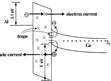
Figure 3 shows the current voltage (I-V) characteristics of Al/ LPD oxide/n-Ge diodes with different oxide thicknesses. The oxide roughness of each sample is also indicated in Fig. 3. Since the oxide thickness is measured by ellipsometry, where the flat interface and surface are assumed, the oxide thickness given here is only for ref-erence. Note that the thickness of really rough oxide is not well defined. The circular areas for all devices are 3.2⫻ 10⫺4 cm2. For sufficiently large negative gate voltage at an inversion condition, the gate current is relatively constant in the log scale. There are two current components in this PMOS diode at inversion bias.15Figure 4 illustrates these two current transport mechanisms. Since the con-duction band discontinuity between Si and Ge is negligible,16 the bandgap difference falls into the valence band discontinuity. Therefore, the valence band barrier height in Fig. 4 is calculated as 5 eV, given a Ge bandgap of 0.66 eV.17The hole current of the
PMOS diode at inversion bias is determined by the minority共hole兲 generation rate in the deep depletion region, because the tunneling rate through the LPD oxide via traps is sufficiently large at large negative gate bias. The hole concentration at the oxide/Ge interface of the PMOS diode is balanced by the thermal generation rate and the tunneling rate through the oxide. As negative gate bias continues to increase, the hole concentration at the oxide/Ge interface in-creases slowly and oxide voltage also inin-creases slightly共soft pin-ning兲. Since the oxide voltage increases slightly with gate voltage, most gate voltage drops on Ge substrates to form deep depletion in Ge substrates. The oxide voltage also causes the tunneling of elec-trons from the Al gate electrode to an n-type Ge substrate. However, the soft pinning of oxide voltage at large negative gate bias restricts the further increase of the electron tunneling current, which is strongly dependent on oxide voltage, and the total inversion current is relatively constant in log scale. In Fig. 3, the inversion current increases with LPD oxide thickness. The mechanism that the thick oxide generates large stress at Ge/SiO2interface, and creates inter-face states may be responsible for this. These interinter-face states gener-ate excessive holes at the interface, and increase the leakage current at the inversion bias.
Figure 1. 共a兲 Experimental flow diagram of the LPD process. 共b兲 The Al/ LPD oxide/n-type Ge MOS devices.
Figure 2. 共a兲 LPD oxide thickness vs. growth time on Si and Ge substrates.
共b兲 Surface roughness vs. LPD oxide thickness on Ge and Si substrates.
Figure 3. I-V characteristics of Ge PMOS diodes with different oxide thick-nesses prepared by LPD.
Figure 4. The schematic diagram of inversion current mechanisms for a PMOS diode. The dark current consists of thermal generated hole current and electron current. Note that the conduction bandedge of Si and Ge are at the same position. Therefore most of the bandgap difference between Si and Ge falls in the valence band discontinuity.
Electrochemical and Solid-State Letters, 6共2兲 F9-F11 共2003兲
F10
The current at an accumulation region 共positive gate voltage兲 shows similar magnitude for different oxide thicknesses. This indicates the transport mechanism is trap-assistant tunneling
共Poole-Frenkel effect兲,18,19when the electrons tunnel from Si to Al at positive gate bias. The tunneling rate through LPD oxide is not thickness-dependent, because the trap in the oxide dominates the tunneling rate through the oxide and the carriers can tunnel through oxide via the assistance of multiple traps.
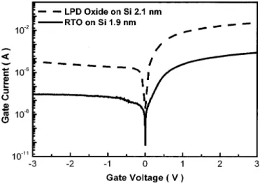
To further confirm our results, the MOS diodes with rapid ther-mal oxide共RTO兲 and LPD oxide on Si were also investigated. Note that no thermal oxide can be grown on Ge substrates. Figure 5 illustrates the I-V characteristics of two these kinds of MOS diodes on Si substrates. The devices areas are 3.2⫻ 10⫺4cm2. The oxide thickness is slightly different. RTO oxide is 1.9 nm and LPD oxide is 2.1 nm. From Fig. 5, the devices with LPD oxide have higher gate leakage current共about two orders of magnitude兲 on both polarities as compared to devices with RTO oxide. The traps in the LPD oxide cause trap-assistant tunneling of gate current, and are responsible for the increase in accumulation current in the LPD oxide. The large interface state density at the Si/LPD oxide interface is responsible for the large inversion current as compared to devices with RTO oxide. Due to the large leakage current, low frequency capacitance-voltage (C-V) and quasi-static C-V cannot be measured,20and the
quantitative value of interface states cannot be determined. In conclusion, a low-temperature LPD process for SiO2 on Ge substrates was well developed. Silicic acid was used to saturate hydrofluorosilicic acid and the time required for solution preparation was only 3 h. At the beginning of the deposition process, the growth rate for LPD oxide on Ge substrates was slow. The surface rough-ness for LPD oxide on Ge was larger than that on Si substrates. The inversion current increased with LPD oxide thickness because the thick oxide generated a large stress at the Ge/SiO2 interface, and created interface states. This LPD process for oxide deposited on Ge can facilitate the integration of SiGe into the Si process.
Acknowledgment
This work is supported by National Science Council, Taiwan, R.O.C. under contract no. NSC 2212-E-002-224 and NSC 90-2212-E-002-226.
National Taiwan University assisted in meeting the publication costs of this article.
References
1. P. Kringhoj, A. N. Larsen, and S. Y. Shirayev, Phys. Rev. Lett., 76, 3372共1996兲. 2. K. Rajendran and W. Schoenmaker, J. Appl. Phys., 89, 980共2001兲.
3. F. Sato, T. Hashimoto, T. Tatsumi, and T. Tashiro, IEEE Trans. Electron Devices,
42, 483共1995兲.
4. Z.-Y. Cheng, M. T. Currie, C. W. Leitz, G. Taraschi, E. A. Fitzgerald, J. L. Hoyt, and D. A. Antoniadas, IEEE Electron Device Lett., 22, 321共2001兲.
5. T. Mizuno, N. Sugiyama, T. Tezuka, and S.-i. Takagi, Appl. Phys. Lett., 80, 601
共2002兲.
6. T. Homma, T. Katah, Y. Yamada, and Y. Murao, J. Electrochem. Soc., 140, 2410
共1993兲.
7. J.-S. Chou and S.-C. Lee, J. Electrochem. Soc., 141, 3214共1994兲.
8. H. Nagayama, H. Honda, and H. Kawahara, J. Electrochem. Soc., 135, 2013
共1988兲.
9. T. Goda, H. Nagayama, A. Hishinuma, and H. Kawahara, Mater. Res. Soc. Symp.
Proc., 105, 283共1988兲.
10. A. Hishinuma, T. Goda, and M. Kitaoka, Appl. Surf. Sci., 49, 405共1991兲. 11. S. Yoshitomi, S. Tomioka, and N. Haneji, Appl. Surf. Sci., 50, 22共1992兲. 12. C.-F. Yeh, C.-L. Chen, and G.-H. Lin, J. Electrochem. Soc., 141, 3177共1994兲. 13. J.-S. Chou and S.-C. Lee, Appl. Phys. Lett., 64, 1971共1994兲.
14. S. Watanabe, N. Nakayama, and T. Ito, Appl. Phys. Lett., 59, 1458共1991兲. 15. B.-C. Hsu, C. W. Liu, W. T. Liu, and C.-H. Lin, IEEE Trans. Electron Devices, 48,
1047共2001兲.
16. C. G. Van de Walle and R. M. Martin, Phys. Rev. B, 34, 5621共1986兲. 17. K. F. Brennan and A. S. Brown, Theory of Modern Electronic Semiconductor
Devices, p. 436, John Wiley & Sons, New York共2002兲.
18. V. Dallacasa and C. Paracchini, Phys. Rev. B, 34, 8967共1986兲.
19. V. Dallacasa and C. Paracchini, IEEE Trans. Electr. Insul., EI-22, 467共1987兲. 20. K. J. Yang and C. Hu, IEEE Trans. Electron Devices, 46, 1500共1999兲.
Figure 5. I-V characteristics of two devices with RTO and LPD oxide.
Electrochemical and Solid-State Letters, 6共2兲 F9-F11 共2003兲 F11