radiation patterns is observed, and front to back ratios of 13 and 11 dB were obtained for the theoretical and experimental results respectively. Both diagrams exhibit a sidelobe
-
5dB down from the mainlobe in the E-plane, which we believe is caused by spuri- ous radiation from the CPW feedline. The measured gain of the antenna at 6 . 7 5 G H z was 7.5dBi.Conclusions: A broadband CPW fed stacked patch antenna was
designed on a high dielectric constant feed substrate with a band- width of &%, and was fabricated and tested. This is a notable improvement in bandwidth over other CPW fed patch antennas. This antenna is suitable for integration with optical modulators, as part of a transducer module for microwave/optical transmission systems requiring a large bandwidth.
0 IEE 1999
Electronics Letters Online No: 19990499 DOZ: IO, 1049/el:19990499
16 March 1999
W.S.T. Rowe and R.B. Waterhouse (Department of Communication and Electronic Engineering, RMZT University, GPO Box 2476 V, Melbourne, VIC 3001, Australia)
E-mail: [email protected]
References
AHMED, Z., NOVAK, D , WATERHOUSE, R.B., and LIU, H.-F.: ‘37GHz
fiber-wireless system for distribution of broad-band signal’, ZEEE Trans., 1997, MTT-45, (8), pp. 1431-1435
coplanar feed line’, ZEEE Microw. Guid. Wave Lett., 1991, 1, (ll), pp. 340-342
GIAUFFRET, L., and LAHEuRTE, LM.: ‘Theoretical and experimental
characterisation of CPW-fed microstrip antennas’, ZEE Proc. Microw. Antennas Propagat., 1996, 143, (l), pp. 13-17
HETTAK, K., DELISLE, G., and BOULMALF, M.: ‘A novel integrated antenna for millimeter-wave personal communications systems’, IEEE Trans., 1998, AP-46, (ll), pp. 1757-1758
LEFORT, G., and RAZBAN, T.: ‘Microstrip antennas printed on lithium niobate substrate’, Electron. Lett., 1997, 33, (9), pp. 7 2 6 727
TARGONSKI, S.D , WATERHOUSE, R.B., and POZAR, D.M.: ‘Design of wide-band aperture-stacked patch microstrip antennas’, ZEEE Trans., 1998, AP-46, (9), pp. 1245-1251
‘High Frequency Structure Simulator Version 5.2’ (Hewlett Packard, 1998)
MENZEL, W., and GRABHERR, W.: ‘A microstrip patch antenna with
CPW-fed slot-loop coupled patch antenna on
narrow substrate
Shih-Wen Lu, Tsung-Fang Huang and Powen Hsu
A coplanar waveguide (CPW) fed rectangular patch antenna excited by a rectangular slot-loop is designed for use in the 2.4GHz ISM band. The size of the slot-loop is chosen to be as close to that of the patch as possible, and the substrate is cut to be as narrow as possible. Experimental results show that this antenna has a nearly omnidirectional pattern in the H-plane and a bandwidth of -22% for VSWR < 2.
Introduction: A simple back-to-back patch antenna fed by a copla-
nar waveguide (CPW) has recently been reported to radiate an omnidirectional pattern in the horizontal plane [I]. This antenna has two identical rectangular patches printed separately on two dielectric substrates, with the CPW and its open-end slot on the ground plane sandwiched in between the two. The two patches are arranged back-to-back relative to the CPW, and the widths of the substrate and the ground plane are cut to be as narrow as that of the patch. It is this narrow width that makes the H-plane pattern of the antenna nearly omnidirectional [l]. This antenna, however, has an inherently narrow bandwidth of -1.7% for VSWR < 2. In this Letter, we propose a CPW-fed slot-loop coupled patch antenna which preserves the omnidirectional pattern but sigdi- cantly increases the bandwidth. The proposed antenna is com- posed only of a rectangular patch and a layer of dielectric substrate. The other patch and substrate in the back-to-back patch
antenna are replaced by a rectangular slot-loop attached to the end of the CPW in the ground plane. The replacement is suitable since the slot-loop is itself a radiating element, and the larger the slot-loop, the more power it radiates to the loop side [2]. The size of the slot-loop is chosen to be as close to that of the rectangular patch as possible so that the radiated power of the slot-loop can be made almost the same as that of the patch. To preserve the omnidirectional pattern in the H-plane, the width of the substrate
is kept as narrow as possible. The input characteristics and radia- tion patterns of this antenna designed for use in the 2.4GHz ISM band are measured and shown in the following.
W
>
substrate
Z
9
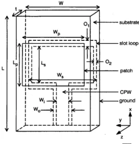
Fig. 1 Configuration of CP W-fed slot-loop coupled patch antenna
Antenna design and experimental results: The antenna configura- tion is shown in Fig. 1. A rectangular patch is placed on one side
of the substrate, while a rectangular slot-loop fed by a CPW is arranged opposite to the patch in the ground plane on the other side of the substrate. The rectangular patch is placed centrally about the rectangular slot-loop, and the size of the slot-loop is made comparable to that of the patch. Experimental models were fabricated on a low cost FR-4 substrate with E, = 4.3, tan6 = 0.02, and t = 1.58mm. Theoretical dimensions of the patch and slot- loop were determined first by setting that both the patch and the slot-loop were resonant at 2.45GHz and by using the moment- method similar to that developed for an infinitely large substrate
[3]. After cutting short the substrate width, resonant frequencies moved lower and higher for the patch and slot-loop, respectively.
-5
I-
4
-25
\
I I I I II
2.2 2.3 2.4 2.5 2.6 2.7 2.8 frequency,GHz
I%
Fig. 2 Measured return loss of CPW-fed slot-loop coupled patch antenna on narrow substrate
Therefore, the lengths and widths of the patch and slot-loop had to be slightly adjusted so that the 2:l VSWR bandwidth of the antenna could cover the entire 2.4GHz ISM band. The final
design parameters used are L, = 2 7 . 5 m , W, = 35.0mm, 0, = 2.0mm, O2
=
0.5mm, L, = 25.7mm and W, = 3 3 . 0 ~ . The widths of the CPW areW; =
3.0mm and WO = 3.6mm, which cor- respond to the characteristic impedance of 50R. The length of the substrate is L = 135.0mm, the width of the substrate is W = 39.0mm, which is only 4.0 mm wider than that of the slot-loop, and the distance between the upper edges of the patch and the substrate is 46.5mm. Return losses of the antenna were measured by using an HP8510B network analyser and adopting the TRL (through-reflect-line) calibration technique, and the measurements were referenced to the end of the CPW line (or the input of the excitation slot-loop). Fig. 2 shows the measured return losses against frequency. The results show that the antenna has a band- width of -22% for VSWR < 2.0. This is more than 12 times largerthan that of the back-to-back patch antenna, which has only 1.7% bandwidth [l].
180"
m
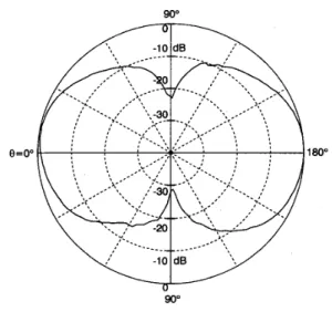
Fig. 3 H-plane patterns of CPW-fed slot-loop coupled patch antenna on narrow substrate, f = 2.45 GHz - co-polarisation _ _ _ _ cross-polarisation 1 80" -10 dB 90" lJdlvllv
Fig. 4 E-plane pattern of CP W-fed slot-loop coupled patch antenna on narrow substrate, f = 2.45GHz
Radiation patterns of the antenna were measured in an ane- choic chamber. The measured H-plane (yz-plane in Fig. 1) pat- terns of both co-polarisation and cross-polarisation are shown in Fig. 3. It is seen that the co-polarisation H-plane pattern is nearly omnidirectional. The variation in the antenna gain is < 3dB. The level of cross-polarisation radiation is at least 9dB lower than that of the co-polarisation radiation. The cross-polarisation arises mainly from the two slots along the x-direction in the slot-loop. For the case where the patch was not used, our other experiment
ELECTRONICS LETTERS
29th April 1999Vol.
35
showed that the cross-polarisation level for the slot-loop alone would be much higher. The E-plane (xz-plane
in
Fig. 1) pattern,as shown in Fig. 4, is a typical sine pattern similar to that of an electric dipole with maxima pointing in the kz directions. Only the co-polarisation pattern is shown in Fig. 4, since the cross-polarisa- tion E-plane pattern is too small to be measured correctly. Com- bining the H- and E-plane patterns, the total radiation pattern of this narrow substrate width, large slot-loop excited, CPW-fed patch antenna is almost the same as that of a dipole antenna.
Compared with the CPW-fed back-to-back patch antenna reported in [l], the CPW-fed slot-loop coupled patch antenna pre- sented above has a better bandwidth performance. The radiation patterns are similar in the two cases. However, the cross-polarisa- tion level is higher in the present case.
Conclusions: Experimental results of a CPW-fed slot-loop coupled
patch antenna fabricated on a narrow-width inexpensive FR-4 substrate for the 2.4GHz ISM band has been described. The pro- posed antenna is low-cost, and has a wide bandwidth and dipole- like radiation pattern. It is suitable for mobile communications, indoor radio, and wireless LAN systems.
0 IEE 1999
Electronics Letters Online No: 19990381 DOZ: 10/1049/el:19990381
4 March 1999
Shih-Wen Lu, Tsung-Fang Huang and Powen Hsu (Department of Electrical Engineering, National Taiwan University, Taipei, Taiwan 1061 7 , Republic of China)
Powen Hsu: Corresponding author
References
1 IWASAKI, H.: 'A back-to-back rectangular-patch antenna fed by a
CPW, ZEEE Trans., 1998, AP-46, (lo), pp. 1527-1530
2 GIAUFFRET, L., LAHEURTE, J.M., and PAPIERNIK, A.: 'Study of various shapes of the coupling slot in CPW-fed microstrip antennas', ZEEE Trans., 1997, AP-45, (4), pp. 642-647
3 DENG, S.M., wu, M.D., and HSU, P.: 'Analysis of coplanar waveguide-
fed microstrip antennas', ZEEE Trans., 1995, AP-43, (7), pp. 73& 737
FDTD
model of scattering from tuned
dielectric strut found in large ground based
radomes
S .
Papadopoulos,C.G.
Parini andJ.
DupuyAn accurate model of dielectric strut scattering using the FDTD method is presented. The strut, formed by joining two radome panels, consists of a dielectric rectangular rod and retaining bolts. Tuning using longitudinal wires embedded in the strut is studied and verified experimentally. Comparison between the FDTD and near-field measurements for a scaled strut model shows very good agreement.
Introduction: Dielectric struts are formed when panels are joined together in the construction of large, ground based, geodesic radomes. The set of struts constitutes the space-frame of the radome. This frame is the main source of coherent scattering that causes degradation of the enclosed antenna's radiation pattern, the scattering from the radome panel being insi&icant in compari- son. With the ever increasing requirements for low sidelobe high performance radome enclosed antennas, there is a need for accu- rate modelling of the effects of strut scattering on the enclosed antenna's far-field radiation pattern.
Some attempts have been made [l, 21 to predict the scattering behaviour of the strut. However the models used did not take into account the details of the strut geometry. In this Letter we describe an FDTD based model, the accuracy of which is con- firmed by near-field measurements.
Modelling of strut and experimental setup: A cross-sectional view
of the actual strut is shown in Fig. la and the gridded FDTD