Digital Signal Processing Engine Design for Polar Transmitter in
Wireless Communication Systems
Hung-Yang Ko, Yi-Chiuan Wang and An-Yeu (Andy) Wu
Graduate Institute of Electronics Engineering, andDepartment of Electrical Engineering, National Taiwan University, Taipei, 106, Taiwan, R.O.C.
Abstract-Polar modulation techniques offer the capability of multimode wireless system and the potential for the high efficiency Power Amplifier (PA). This paper describes a new design of Digital Signal Processing (DSP) engine for the polar transmitter. The digital part includes rectangular-to-polar converter and digital phase modulator, and the engine is designed for EDGE (2.5G) system. We employ the Coordinate Rotation Digital Computer (CORDIC) and Direct Digital Frequency Synthesizer (DDFS) techniques in our design. A prototype chip has been designed and fabricated in UMC 0.18 um CMOS process with 1P6M technology.
1. INTRODUCTION
Polar modulation offers the capability of achieving high linearity and high efficiency simultaneously in a wireless transmitter. Improved efficiency is achieved by using a highly efficient and non-linear PA to work at its peak efficiency. Linear transmission is achieved by modulating the envelope of the signal through the voltage supply of the PA.
Polar transmission utilizes envelope and phase component to represent the digital symbols instead of the conventional I/Q format [1]. The baseband signal V(t) is split into the phase signal
θ(t) and the envelope signal A(t).
).
(
)
(
)
(
t
x
t
j
y
t
V
=
+
⋅
(1).
)
(
)
(
tan
)
(
,
)
(
)
(
)
(
1 2 2
=
+
=
−t
x
t
y
t
t
y
t
x
t
A
θ
(2)It is clear that from Eq. (2) we can have a phase-only signal through phase modulator and multiplied with its envelope at the PA to recreate the original complex signal V(t). This polar modulation process is like the Envelope Elimination and
Restoration (EER) [2] architecture. In the conventional design,
one part goes through a limiter to remove the envelope and keeps the phase information only. And the other part is detected by an envelope detector to extract the envelope information.
This work is supported by the MediaTek Inc., under NTU-MTK wireless research project.
But both circuits would suffer from the non-linearity and distortion of the analog devices and would cause mismatch
problem through the two paths. In this paper we proposed a DSP engine which includes rectangular-to-polar converter and digital
Phase Modulator (PM). The design does not have the distortion
problem caused by the analog components and the phase modulation process can be precisely controlled by the digital phase modulator. The baseband phase signal is modulated through digital phase modulator at the specific frequency range. The phase modulated signal is represented as SIF-PM(t).
)).
(
cos(
)
(
t
w
t
t
s
IF−PM=
c+
φ
(3)The PA stage of amplitude modulator (AM) operates in principle as a multiplier in our design model. This gives the output signal in the specific frequency band as follows:
{
}
).
sin(
)
(
)
cos(
)
(
,
Re
)
(
),
(
)
(
)
(
) (t
w
t
y
j
t
w
t
x
e
e
t
A
t
s
t
A
t
s
c c t jw t j PM IF IF c⋅
+
=
⋅
⋅
=
⋅
=
− φ (4)For convenience of the simulation model [2], the gain of the PA is set to one. Thus the Eq. (4) is equal to the signal of EDGE, which is up-converted at Intermediated Frequency (IF) band. The non-linearity of PA and analysis of up-converter to Radio Frequency (RF) stage are beyond the scope of this paper.
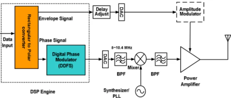
Fig. 1. Architecture of polar transmitter.
2. POLAR TRANSMITTER ARCHITECTURE
The architecture of the polar transmitter is shown in Fig. 1. The rectangular-to-polar converter extracts the symbol phase and envelope information in the digital domain. Then the phase information is modulated through digital phase modulator to create a constant envelope and phase modulated signal. The phase modulated precision and channel selection can be well controlled in the digital part first. In this paper we use the concept from [3] to realize the digital phase modulator design. The digital fine-tune frequencies are generated by the DDFS. The DDFS interpolates
6026
0-7803-8834-8/05/$20.00 ©2005 IEEE.
the carrier frequencies between the coarse frequencies generated by the integer-N PLL. The main design considerations of the DSP engine include: (a) the bandwidth of the envelope and the phase signal; (b) the numbers of the fine-tune frequencies generated by the DDFS would affect the clock rate of DDFS and rectangular-to-polar converter; (c) the quantization effect in digital domain will cause phase noise and frequency spurs. And this effect also influences the Error Vector Magnitude (EVM) performance and the signal spectrum. Typically the bandwidths of envelope and phase signal are equal to 1~2 MHz and larger than the EDGE signal bandwidth 200k Hz. The clock rate of the DDFS can be derived [3] as below:
)
2
)
1
(
(
4
.
0
1
tb cs sym clkf
N
f
f
S
f
=
⋅
>
⋅
×
+
+
(5)Where fclk is the clock rate of DDFS, S is the number of samples
per symbol and fsym is the symbol rate of the EDGE signal. The
maximum output frequency of DDFS is limited to 0.4 times the clock frequency. The parameter fcs is the carrier spacing (200 kHz)
in EDGE system, N is the number of digital fine tune frequency and ftb is the transition BW of the filter which is located after
up-converter stage. In our design, we choose N=25, ftb=10 MHz,
fcs=200 kHz and S=96. Thus the clock rate of DDFS should be
operated at 26 MHz. The digital fine tuning frequencies are generated by the DDFS and locating at 5 MHz~10.4 MHz. Each interpolated frequency (channel) is stored in the fine-tune
Frequency Control Word (FCW) table.
3. RECTANGULAR-TO-POLAR CONVERTER
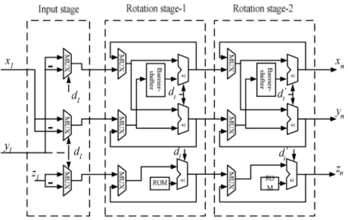
For a coordinate axis converter, we adopt the CORDIC algorithm in our design since the CORDIC algorithm is very simple and low hardware cost. In order to further reduce the complexity, we also apply the technique in [4] to our rectangular-to-polar converter. For the first iteration we move the input vector into 1-th and 4-th
quadrant with simply sign inversing and data exchanging. Second we replace yi by yi·2-i as compared with conventional CORDIC
algorithm. This modification can save once iteration and one barrier shifter in the rectangular-to-polar converter. This can save more area in our design. For i=1 and input vector is (x1, y1) from
the EDGE signal:
.
5
.
0
,
,
1 2 1 1 2 1 1 2d
z
x
d
y
y
d
x
⋅
=
⋅
−
=
⋅
=
.
0
,
1
0
,
1
)
(
≥
<
−
=
=
i i i iy
y
y
sign
d
(6)And the remaining iterations (for i=2~n) are shown in Eq. (7).
[
]
.
,
2
,
2
1 1 ) 2 ( 2 1 i i i i i i i i i i i i ip
d
z
z
x
d
y
y
y
d
x
x
⋅
+
=
−
⋅
=
⋅
⋅
+
=
+ + − − + (7).
2
1
1
),
2
(
tan
1
) 2 ( 2 ) 2 ( 1∑
− − − − −+
=
⋅
=
i i i iK
p
π
The desired phase is zi+1 and the desired envelope value is xi+1
multiplied by a constant scaling factor K. Due to the iterative feature of CORDIC algorithm, the clock rate of this module is n*fclk, and n is iteration number. It is hard for the module to
operate at such high clock rate. A compromise is to use unfolded technique and the architecture is shown in Fig. 2.
± ± ± ± ± ±
Fig. 2. Architecture of rectangular-to-polar converter.
4. DIGITAL PHASE MODULATOR
⊕
mod−4πFig. 3. Architecture of DDFS
The DDFS architecture is shown in Fig. 3. The DDFS has three basic blocks: FCW table, phase accumulator and phase-to-amplitude converter. The FCW table stores the desired fine-tune frequency control words and can be derived from Eq. (8).
1
2
,
2
−<
∀
⋅
=
L L clk cFCW
f
FCW
f
(8)In our design we focus on the phase-to-amplitude converter design and propose an architecture which is based on Least
Squared (LS) algorithm [5] and Merged-Multiply Accumulator
(MAC) technique [6]. The input phase is first truncated by 3-bit according to the π/4 symmetry and the amplitude of the sine
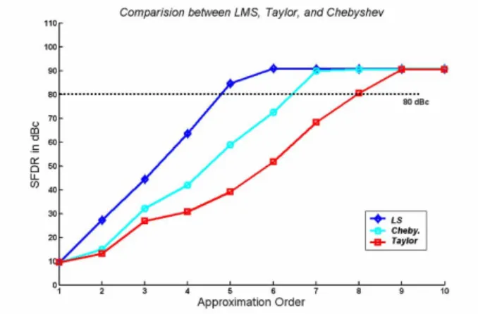
function can be express by the polynomial. The approximated polynomial is generated according to the LS algorithm. In this paper we compare the Spurious Free Dynamic Range (SFDR) performance with the other approximation algorithm such as Taylor and Chebyshev [9]. The comparison method is set the input phase from 0 to π/2. The phase word-length is 15-bit and amplitude output is 15-bit. From the simulation result in Fig. 4, we can easily see that the LS-based polynomial can achieve better performance than Taylor and Chebyshev approximation algorithm with less polynomial order. The less order of polynomial means that low hardware complexity can also be achieved.
Fig. 4. SFDR comparison between LS, Taylor and Chebyshev. In order to reduce the polynomial order we further divide the approximated region into eight segments. In each segment, the approximated polynomial p(X) can be represented as in Eq. (9).
). ] 2 _ [ 2 / 0 [ ] 4 ] 1 _ ([ 1 0 2 ] [ ] [ 1 0 2 ) ( 4 2 3 1 4 3 2 1 1 0 1 2 2 n rom n j Q X n n rom MAC n k C n X n c n i R c X c X c X p j j k k i i + ∑ = ⋅ ⋅ + = ∑− = ⋅ + ⋅ + ∑− = ⋅ = + ⋅ + ⋅ = (9)
[ ]
: . , 0 1 , 0 , 2 1 , 1 , 1 1 2 , 1 2 , 1 1 2 , 1 bit n with truncation the denote c and c c c c Q n j j j j j − = = + + − = − − + (10)Where ci represents the coefficient, and X is the phase of each
divided region. In Eq. (9) we store the first term and third term in the look-up table. The size of rom_1 and rom_2 are 1,536 bits and 232 bits respectively. The operations in Eq. (9-10) now become one booth multiplication and two constant additions. These can be merged into a modified-MAC (Fig. 4).
First the binary phase X is inputted to the booth decoder circuit and the partial product term is generated in each row of MAC. The partial product terms are summed through Carry-Save-Adder (CSA) tree. As compared with the direct implementation of 2th
order polynomial, the CSA tree can prevent the carry ripple problem in the early stages, and the carry ripple only occurs at the final stage. Due to the EDGE spectral requirement we target the desired SFDR over 80dBc. From Matlab simulation, we set the
truncated accumulated phase word-length to W=15 bits and amplitude word-length to P=14 bits. These hardware parameters can achieve SFDR=86dBc. The other parameter is the word-length of the phase of the EDGE signal. This will also introduce phase noise and spurs in the output spectrum and we will discuss in section 5. The proposed DDFS circuit is simulated by the
NANOSIM tool and compares with state of the art in Table 1. It is
obvious that the proposed DDFS can achieve high SFDR performance. The power efficiency is also superior to the other designs. 15 C C14C13C12C11 C8 C7 C5 C4 0 C 6 C 10 C C9 C3 1 C 2 C 2 R R1 3 R 4 R 5 R R0 0 P 1 P 2 P 3 P 4 P 5 P 6 P 7 P 8 P 9 P 10 P 11 P 12 P 13 P 14 P 15 P 16 P 17 P 18 P 19 P 20 P 21 P 22 P 23 P
Fig. 4. Architecture of Modified-MAC.
Table 1. Comparison with the existing DDFS designs.
DDFS CMOS tech. SFDR Latency efficiency Power (mW/MHz) Ours 0.18 86 5 0.15 Ref [7] 0.18 84 - 0.22 Ref [8] 0.25 90.3 13 0.66 Ref [9] (Taylor) 0.35 82.5 9 0.26 Ref [9] (Chebyshev) 0.35 73 7 0.35 Ref [10] 0.35 80 2 0.44 5. SIMULATION RESULT
For Mobile Station (MS), the requirements of EVM-rms and EVM-peak are below 9% and 30%. For Base-Tranceiver Station (BTS) EVM-rms and EVM-peak are below 7% and 22%. The SFDR performance of the digital frequency synthesizer is suitable for the up-link and down-link spectral requirement. But the phase signal word-length also contributes spurs and phase noise. And the wordlength also affects the EVM and the signal spectrum. In this paper we simulate the finite word-length (J) effect of the phase signal with the EVM measurement and spectral mask requirement. The performance summary is in Table 2.
Table 2. Simulation result and EVM measurement.
J-bits EVM-rms EVM-peak Spectral requirement
9-bits 0.028% 0.094% No (Spurs at -66dBc)
10-bits 0.014% 0.046% No (Spurs at -74dBc)
11-bits 0.007% 0.018% No (Spurs at -79dBc)
12-bits 0.003% 0.011% Yes (Spurs at -81dBc)
From the Table 2, we can see that the errors produced by the phase quantization are very small for the word-length higher than 9-bits. And the errors introduced by the entire digital phase modulator can be eliminated. But the spectrum of the SIF-PM(t)
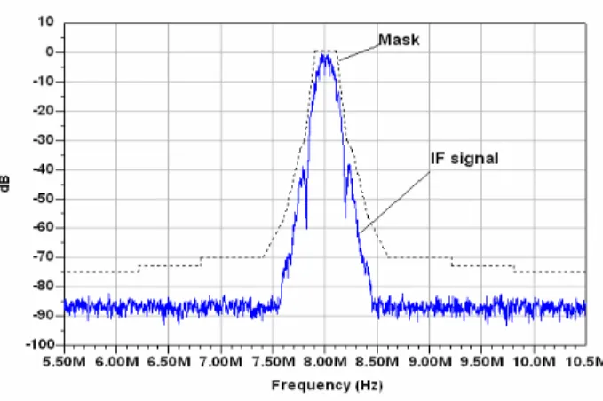
signal is not exactly below the spectral mask. Especially for BTS-mask, the requirement of the mask is more stringent than MS-mask. Since the quantization phase error will degrade the synthesizer SFDR performance. It is conservative to choose J=12-bit in our design. The signal spectrum with J=12-J=12-bit at the carrier which equals to 8 MHz is shown in Fig. 5. The digital phase modulated signal generated by the DDFS can meet the spectral requirement for BTS-mask and MS-mask.
Fig. 5. The spectrum of the EDGE signal through DSP engine.
6. IMPLEMENTATION RESULT
The proposed DSP engine was implemented in UMC 0.18 um CMOS process with 1P6M technology. The layout of the DSP engine is shown in Fig. 6. The summary of the circuit is list in Table 3.
Fig. 6. layout of the proposed DSP engine.
Table 3. Implement summary of the DSP engine.
Technology UMC 0.18 um 1P6M CMOS
Voltage 1.8 V
Core layout area 0.51x0.51 mm2
Chip layout area 1.114x1.114 mm2
System clock Frequency 26MHz
Power
consumption@26MHz 3.92 mW
7. CONCLUSION
In this paper, we proposed the DSP engine for the polar transmitter. The engine is realized by the CORDIC and DDFS techniques. In the digital phase modulator we adopt the LS algorithm. We also apply MAC technique in our DDFS architecture to reduce the hardware complexity and decrease the carry ripple problem of the direct polynomial implementation. The chip implementation with UMC 0.18 um CMOS process with
1P6M technology is also presented in this paper.
8. REFERENCES
[1] Nagle, P.; Burton, P.; Heaney, E.; McGrath, F., “A wide-band linear amplitude modulator for polar transmitters based on the concept of interleaving delta modulation,” IEEE
Journal of Solid-State Circuits, vol. 37, pp. 1748-1756, Dec.
2002.
[2] Rudolph, D.; “Out-of-band emissions of digital transmissions using Kahn EER technique,” IEEE Trans., Microwave Theory and Techniques, vol. 50, pp. 1979-1983. Aug. 2002.
[3] Vankka, J.; “Digital frequency synthesizer/modulator for continuous-phase modulations with slow frequency hopping,” IEEE Trans., Vehicular Technology, vol. 46, pp. 933-940, Nov. 1997.
[4] Chen, A.; Yang, S.; “Reduced complexity CORDIC demodulator implementation for D-AMPS and digital IF-sampled receiver,” in Proc. Globecom `98, vol.3, pp.1491-1496, Nov. 1998.
[5] M. Flickner, J. Hafner, and E.J. Rodriguez, and J.L.C. Sanz; “Fast least-squares curve fitting using quasi-orthogonal splines,” IEEE Int. Image Processing, vol. 1, pp. 686-690, Nov. 1994.
[6] Elguibaly, F.; “A fast parallel multiplier-accumulator using the modified Booth algorithm,” IEEE Trans., Circuits and
Systems, vol. 47 , pp. 902-908 , Sept. 2000
[7] Langlois, J.M.P.; Al-Khalili, D.; “Low power direct digital frequency synthesizers in 0.18 /spl mu/m CMOS,” IEEE
CICC Proceedings, pp. 21-24, Sept. 2003.
[8] A. Torosyan, Dengrwei Fu, Jr. Willson A. N., “A 300 MHz quadrature direct digital synthesizer/mixer in 0.25 µm CMOS,” in IEEE Solid-State Circuits Conference, vol. 1, pp. 132 -133, 2002.
[9] Kalle I. Palomaki and Jarkko Niittylahti; “Phase-to-Amplitude Mapping in Direct Digital Frequency Synthesizers Using Series Approximation,” EURASIP Journal on Applied
Signal Processing, 2001.
[10] D. De Caro, E. Napoli, A. G. M. Strollo, “Direct digital frequency synthesizers using high-order polynomial approximation,” IEEE Solid-State Circuits Conference, vol. 1 , pp. 134 -135, 2002.