This content has been downloaded from IOPscience. Please scroll down to see the full text.
Download details:
IP Address: 140.113.38.11
This content was downloaded on 26/04/2014 at 10:06
Please note that terms and conditions apply.
Fabrication of single-crystal tin nanowires by hydraulic pressure injection
View the table of contents for this issue, or go to the journal homepage for more 2006 Nanotechnology 17 367
(http://iopscience.iop.org/0957-4484/17/2/004)
Nanotechnology 17 (2006) 367–374 doi:10.1088/0957-4484/17/2/004
Fabrication of single-crystal tin nanowires
by hydraulic pressure injection
Chien-Chon Chen
1, Y Bisrat
2, Z P Luo
3, R E Schaak
4, C-G Chao
1and D C Lagoudas
2,51Department of Materials Science and Engineering, National Chiao Tung University,
Hsinchu, Taiwan
2Department of Aerospace Engineering, Texas A&M University, College Station,
TX 77843-3141, USA
3Microscopy and Imaging Center, Texas A&M University, College Station,
TX 77843-2257, USA
4Department of Chemistry, Texas A&M University, College Station, TX 77843-3141, USA
E-mail: [email protected]
Received 15 September 2005, in final form 8 November 2005 Published 14 December 2005
Online atstacks.iop.org/Nano/17/367
Abstract
Tin (Sn) nanowires, with 15 and 60 nm average diameter and up to 10µm in length, were fabricated by an injection process using a hydraulic pressure method. The Sn melt was injected into an anodic aluminium oxide (AAO) template and solidified to form nanowires. By back etching the aluminium substrate and barrier layer, the nanowire array ends were partially exposed from the bottom face of the AAO template. The filling ratio of nanowires inside and through the thickness of the AAO template was found to be close to 100%. The nanowires were also found to be dense and continuous with uniform diameter throughout their length. Transmission electron
microscope (TEM) and x-ray diffraction (XRD) studies on the 60 nm diameter nanowires revealed that the nanowires were single crystals with body-centred-tetragonal (bct) structure predominantly growing along the [100] direction. The current method of synthesizing nanowires is straightforward, low-cost and suitable for low-melting point (<650◦C) metals including low-melting point alloys with stoichiometric composition.
1. Introduction
With the continued demand for miniaturization of electronic and optical devices, nanowires with enhanced mechanical and electrical properties are needed. To develop scaled-up functional devices highly ordered nanowire arrays are essential. Many candidate materials (metals, alloys, metal oxides and semiconductors) have been studied for various potential applications in nanotechnology and have shown some promising results [1–12]. Further developing methods to synthesize nanowires cheaply and efficiently is of paramount importance for manufacturing future generation nanodevices. In this work, tin (Sn) nanowires were fabricated using a pressure injection method, and their properties were characterized. The study of Sn nanowires has been motivated
5 Author to whom any correspondence should be addressed.
by the attractive properties of bulk Sn and the novel properties of nanostructures such as nanowires. Bulk Sn has excellent ductility, electrical conductivity, resistance to corrosion and has been extensively used in the electronics industry [13–17]. Sn-based alloys are also among the most promising lead-free solders. On the other hand, recent experimental studies have shown some unique superconductivity and magnetization properties of Sn nanowires [11,18,19]. In addition, through oxidation of Sn nanowires, sensitive single SnO2nanowires
can be synthesized for gas sensors [20]. Therefore, it is of interest to investigate whether cost-effective and efficient manufacturing methods for Sn nanowires maintain or even enhance the physical properties of bulk Sn at the nanoscale.
Metallic nanowires, including Sn, have been widely produced by the electrodeposition process [8,9,11,13,19–23] using anodic aluminium oxide (AAO) templates. Relative to other deposition techniques such as chemical vapour
C-C Chen et al
deposition (CVD), the electrodeposition technique has been proven to be a low-cost and a high-yield method for producing nanowires from different materials [23]. However, there are some drawbacks associated with most electrodeposition processes, including lack of nanowire length uniformity and length control. Another major challenge with electrodeposition is that the success of the process is highly dependent on finding the appropriate chemical precursor. Finally, most electrodeposition methods require a conducting substrate or catalyst which may jeopardize the purity of the nanowires. A different approach that has been utilized for fabricating metallic nanowires and which overcomes most of the problems associated with deposition processes is based on an injection method. In this method, a molten metal is impregnated into the nanochannels of the AAO template. The nanowires that result from an injection process are continuous, dense and have uniform diameter along the length of the wire. Various metallic nanowires (Sn, Bi, Al, In) with diameters larger than 200 nm have been fabricated by the injection method [24]. Recently, the use of a high-temperature gas pressure chamber has enabled the injection of bismuth (Bi) melt into AAO templates as small as 13 nm in diameter [25,26]. It should be noted that the main challenge in the injection process is the high external pressure required to overcome the surface tension of the molten metal to fill the nanochannels. The smallest diameter nanochannel that can be filled is constrained by the maximum pressure the gas chamber can sustain and operate at safely. When a pressure higher than the chamber maximum is necessary, wetting agents with poor solubility in the molten metal are added to lower the surface tension of the molten metal and hence reduce the required injection pressure [26]. This article presents a hydraulic pressure injection method as an alternative to the aforementioned gas pressure injection, capable of achieving higher pressure ranges to inject molten Sn into nanochannels as small as 15 nm in diameter, without the aid of a wetting agent. The injection process is simple enough that it could be easily set up in a conventional laboratory whereby the vacuum chamber is heated by a hot plate and the external pressure is delivered through a hydraulic jack.
The fabrication of Sn nanowires and their structural characterization are the focal points of this paper. A brief summary of the fabrication process of the AAO template is given in section 2.1. A description of the experimental procedure of the hydraulic injection method used in this work and the fabrication of Sn nanowires are presented in section 2.2. The performance of the current injection procedure and comparisons with the gas pressure injection method are discussed in sections 3.1 and 3.2. The experimental observations and the results obtained from various characterization methods are given in section 3.3. Finally, section 4 presents a brief summary of the most important results and some key conclusions.
2. Experimental procedure 2.1. Fabrication of AAO template
Anodic aluminium oxide (AAO) templates with average channel diameter of 60 and 15 nm and thickness of 10 µm
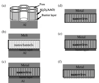
Metal nanowires Metal nanowires nanowires barrier layer Metal Barrier layer nanochannels barrier layer Al Melt Al nanowires barrier layer Metal Al2O3(AAO) Al Pore Metal nanowires Metal nanowires Metal nanowires Metal nanowires nanowires barrier layer Metal nanowires barrier layer Metal Barrier layer nanochannels barrier layer Al Melt nanochannels barrier layer Al Melt Al nanowires barrier layer Metal Al nanowires barrier layer Metal Al2O3(AAO) Al Pore Al2O3(AAO) Al Pore (a) (d) (b) (e) (c) (f)
Figure 1. Schematic representation of the step-by-step fabrication procedure: (a) formation of porous alumina layer (AAO), the Al substrate remained attached to the AAO template during the injection process, (b) set-up before injection, (c) nanowires formed after injection, (d) Al substrate removed, (e) barrier layer removed and (f) ends of nanowires exposed after partial removal of the AAO template.
were fabricated by one-step anodization. The templates were generated by anodizing a commercial aluminium (Al, 99.7%) substrate. The Al substrate was first electro-polished in a bath consisting of 15% perchloric acid (HClO4, 70%),
70% ethanol (C2H6O, 99.5%) and 15% monobutylether
((CH3(CH2)3OCH2CH2OH), 85%). The 60 nm pore diameter
template (denoted as AAO60 hereafter) was then fabricated by anodizing the polished Al substrate at 40 V in 3 vol% oxalic acid ((COOH)2, 99.9%). The anodization for the
15 nm pore diameter template (denoted as AAO15 hereafter) was performed at 18 V in 10 vol% sulfuric acid (H2SO4,
98%). More detailed description of the process can be found elsewhere [27]. It should be noted that the Al substrate was not removed after anodization; it was kept to serve as padding for the fragile porous AAO template during the injection process.
2.2. Fabrication of nanowires by hydraulic pressure injection
An outline of the step-by-step fabrication procedure of the Sn nanowires is presented in figures1(a)–(f). The nanowires were fabricated by vacuum melting and pressure injection of the Sn melt into the nanochannels of the AAO template. The vacuum hydraulic pressure injection set-up has been described previously [28]. The pressure (P) needed for the Sn melt to be impregnated into the nanochannels was estimated by the simplified Washburn equation given by P = −4γ cos θ/D, whereγ is the surface tension of the melt, θ is the contact angle between the template and the melt, and D is the diameter of the channel [26]. In the current study, γ of Sn was taken to be 0.544 N m−1 [29], and θ for molten Sn on alumina substrate was taken to be 158◦–173◦ [30]. Figure 2shows the plot of the external pressure estimated from the Washburn equation for molten Sn as a function of channel diameter for
θ = 165◦ (taking an average from the given range). The
external pressure for the AAO60 and AAO15 templates was estimated to be∼350 and ∼1400 bar, respectively. As can also 368
10 20 30 40 50 60 70 80 90 100 channel diameter (nm) Ap p lie d p r es su re (b a r ) Contact angle, = P ~ 350 bar (AAO60) P ~ 1400 bar (AAO15) 0 300 600 900 1200 1500 1800 2100
Figure 2. A plot showing the estimated external pressure as a function of channel diameter from the simplified Washburn equation [25] for molten Sn assuming a contact angle of 165◦. The black arrows correspond to the estimated pressure values for AAO15 and AAO60 templates.
be seen from the plot, the injection pressure increases steeply as the diameter decreases, especially for nanochannel diameter less than 30 nm.
For the fabrication of Sn nanowires, a disc-shaped Sn foil (whose diameter and thickness were 10 and 2 mm respectively) was placed on the top side of the AAO template and both were put inside a mould. The mould, containing the AAO/Sn foil, was then placed inside a vacuum chamber and heated up to the melting temperature of Sn (∼230◦C) using a hot plate. The hot chamber was removed from the hot plate and pressure was applied on the melt, through the sliding column of the chamber, using a hydraulic jack to impregnate the molten Sn into the nanochannels of the AAO template. The injection process was completed in less than a minute and the chamber was immediately placed in cold water to cool down for a period of 10–15 min to solidify the impregnant inside the nanochannels. Several samples were prepared this way by varying the applied pressure between 350 and 700 bar for the AAO60 template and 1–1.5 kbar for the AAO15 template.
The filling ratio of the hydraulic injection method was investigated by examining the top and bottom surfaces of the Sn-filled AAO template using a scanning electron microscope (SEM). The top face of the AAO template was studied after mechanically removing (peeling by hand) the excess surrounding bulk Sn from the top surface of the Sn-filled AAO template. To examine the bottom surface of the AAO template, the Al substrate was first removed with a CuCl2-based solution [31] which revealed the barrier layer
that capped the nanochannels. The barrier layer and a few nanometres of AAO template were etched away using NaOH solution which exposed the ends of the nanowires. These etching procedures and the resulting morphologies of the bottom surface will be illustrated in more detail in section 3.2. Free-standing Sn nanowires were collected after the AAO template was dissolved thoroughly in 0.4 M
H3PO4+ 0.2 M CrO3mixture solution at∼60◦C for 1 h [31].
Repeated sonication, centrifugal sedimentation, decanting of the supernatant and rinsing with ionized water removed the excess H3PO4–CrO3mixture. The released nanowires were
suspended in isopropanol and dispersed by sonication. A drop of the suspension was then deposited onto a Cu grid with carbon
film and left to dry prior to transmission electron microscope (TEM) or SEM observation.
The structure and morphology of the Sn nanowire arrays were studied using various methods. The morphology of the top and bottom surfaces of Sn-filled AAO template, after the injection process and various etching procedures, were studied using an SEM (FE-SEM, Zeiss 1530). The crystal structure of the Sn nanowire arrays was determined by using an advanced powder diffractometer (Cu Kα1) fitted with a Ge
monochromator and a position-sensitive detector in Bragg– Brentano geometry (XRD, Bruker D8). Differential scanning calorimetry (DSC, PerkinElmer Pyris 1) was used to determine the melting point of both the precursor bulk Sn and Sn nanowire arrays. A TEM (JEOL 2010) was employed to characterize the crystallinity and growth orientation of free-standing Sn nanowires. The experimental observations and results will be presented and discussed in the next section.
3. Results and discussion 3.1. Sn nanowires
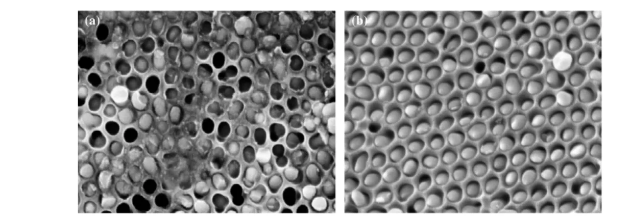
Figure 3shows SEM micrographs of the top surface of an AAO60 template after the injection of molten Sn. When the applied pressure was equal to the estimated value (350 bar), the filling ratio was found to be only about 60% (figure3(a)). The filling ratio improved to almost 100% (figure 3(b)) by increasing the applied pressure to about 700 bar. Even though other pressure values between 350 and 700 bar might have equally improved the filling ratio, because 700 bar was within the capability of the apparatus, a decision was made to double the applied pressure in order to ensure the maximum filling ratio. One plausible explanation why a higher pressure value than the value estimated from the analytical expression (Washburn equation) was needed for complete filling is the possibility of not having complete molten state of the Sn metal just before injection. Although the nominal reading of the thermocouple in the apparatus was the expected melting temperature of Sn, the position of the thermocouple inside the chamber and possible thermal gradients in the chamber may have led to a thermocouple reading overestimating the actual temperature of the Sn metal.
3.2. Investigating the filling ratio
The bottom surface of the Sn-filled AAO was examined in order to ensure the filling of the pores all the way through the thickness of the AAO (10 µm) template. Hence, the Al substrate was removed by using a CuCl2-based solution
at 25◦C for 3 min that subsequently revealed the barrier layer [31]. The barrier layer was then etched away using 5 vol% H3PO4 at 23◦C for 20 min to expose the ends of
the nanowires. The 20 min etching time only removed grain boundaries of the barrier layer but did not open the capped ends. The etching time was increased to 180 min but the acid solution appeared to have reacted with the Sn nanowires and instead of pore opening it resulted in a smeared surface. The 5 vol% H3PO4solution that has been widely used for removing
barrier layer and pore opening of the bottom surface of an empty template did not seem to work well for a metal-filled template. Consequently, to selectively dissolve the barrier
C-C Chen et al
(a) (b)
Figure 3. SEM micrograph taken from the top surface of AAO60 samples injected with applied pressure of (a) 350 bar and (b) 700 bar.
layer without affecting the Sn nanowires, sodium hydroxide (NaOH) solution was used in place of H3PO4. After trying
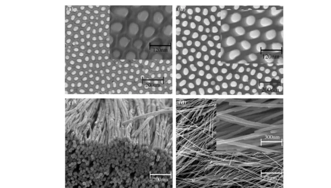
a range of concentration levels of NaOH (0.1–10 wt%), it was found that 0.2 wt% gave the required degree of control for the step-wise removal of the AAO template. Figure 4
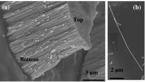
shows the ends of the nanowires exposed after the barrier layer was etched away by 0.2 wt% NaOH at 23◦C for 150 min. The dark regions indicate empty pores and the white regions indicate Sn-filled pores. Relative to the top surface of the Sn-filled template (figure3(b)), the bottom surface had close to 25% empty nanochannels, indicating the Sn melt did not permeate all the way through the thickness of the template for some nanochannels (figure 4). The moisture and gases retained in the AAO nanochannels during post-anodization treatments might have obstructed the impregnation of the Sn melt through the thickness of the AAO template. Therefore, post-anodization treatment was carried out on AAO templates before the injection process to eliminate the potential problem of trapped air/moisture pockets. Figures5(a)–(f) show SEM micrographs taken from the bottom surface of various Sn-filled AAO60 templates, that have undergone post-anodization treatment of drying and degassing at high temperature prior to the injection of molten Sn for the same injection pressure of 700 bar. The number of empty nanochannels (darker regions) was notably high for the as-anodized template injected with Sn melt (figure5(a)). When the template was dried at 450◦C for 1 h in air, the filling ratio improved only slightly, as shown in figure 5(b). However, after drying (450◦C, for 1 h) and degassing (10−3Torr) the filling ratio improved considerably. The optimal degassing time was obtained after investigating various time intervals as shown in figures5(c)–(f). It was found that 25 min of degassing time yielded almost 100% of Sn melt impregnation through the template thickness (10 µm). The continuity of the nanowires through the thickness of the AAO template was also confirmed by studying the cross-section of nanowire arrays by SEM (figure6(a)). Figure6(b) shows a freestanding 10µm long Sn nanowire. In comparison to the recent gas pressure method [26] where a total time of 10 h was required for degassing (at 250◦C) and drying (at 350◦C) the template prior to injection, the current method required a total time of 85 min for the same procedure. The capability of the apparatus in the current method to go to higher temperature (450◦C) for the post-anodization treatment prior to injection helped in improving the permeation of molten Sn through a
180 nm Figure 4. SEM image of the bottom surface of an AAO60 sample after removal of the barrier layer with 0.2 wt% NaOH showing Sn-filled (white regions) and empty (black regions) nanochannels.
thickness of 10µm by removing moisture and air pockets in a short period of time.
Studies were carried out to find a suitable condition to completely remove the barrier layer and partially etch away the Sn-filled AAO template in order to expose standing ends of nanowires in a controlled manner for future physical property probing. Figure7shows a range of etching times and their corresponding morphologies for AAO60 that was etched by 0.2 wt% NaOH at 23◦C. When the barrier layer was etched for 120 min, nanochannels were opened exposing the tips of the nanowires, as shown in figure7(a). Increasing the etching period to 150 min dissolved the barrier layer completely and the tips of the nanowires stuck out a few nanometres (figure7(b)). As the etching time was further increased to 180 min, the pore walls started to break down, leading to Sn nanowires adhering to each other (figure7(c)). The AAO template was completely dissolved after 210 min of etching and the nanowires collapsed on the Al substrate as shown in figure7(d).
Similarly, the morphologies of the etchings of Sn-filled AAO15 template are illustrated in figure8. Since the barrier layer of the AAO15 template was thinner than that of the AAO60 template, the etching time required to expose the nanowire tips after completely removing the barrier layer of the AAO15 sample was 30 min (figure 8(a)), in contrast to the 150 min needed for the AAO60 sample (figure 7(b)). The thickness of a barrier layer is determined mainly by the anodizing voltage although there is a slight deviation 370
Figure 5. SEM images of the bottom surfaces of AAO60 samples showing the effect of drying and degassing the template before injection, where the black regions denote empty nanochannels while white regions indicate Sn-filled nanochannels. Low filling ratio was observed in the absence of drying and degassing (a); this then improved slightly after drying at 450◦C for 1 h only (b); and continued to progressively improve after drying at 450◦C and degassing for (c) 10 min, (d) 15 min, (e) 20 min and (f) 25 min.
Bottom
3 m Top
2 m
(a) (b)
Figure 6. SEM micrograph of (a) the cross section of the AAO60 sample with dense, continuous nanowire arrays stretching all the way through the thickness of the template, and (b) single 10µm long Sn nanowire after released from the AAO template.
depending on the anodization electrolyte and temperature. Early experimental studies on the morphology and mechanism of pore formation on aluminium films showed that the barrier layer thickness is proportional to the anodization voltage [32]. According to the correlation between the barrier layer thickness and anodizing voltage given in the
literature [32], the thickness of the barrier layer of the templates used in this study are estimated to be∼18 nm and ∼40 nm for AAO15 and AAO60 templates respectively, and hence the significant difference in etching time.
3.3. DSC, TEM and XRD studies of nanowires
Differential scanning calorimetry (DSC) studies were carried out to examine the size-dependent and dimension-dependent melting behaviour of Sn nanowires embedded in the AAO template. Figure 9 compares results of the Sn nanowires embedded in the AAO matrix with that of bulk Sn. The melting point shows a slight reduction as the nanowire diameter decreases from 60 to 15 nm. Various researchers [33–36] have shown that low-dimensional crystals, including metallic nanocrystals, embedded in a matrix can melt below or above the melting point of their corresponding bulk crystal. The embedded nanocrystals could be spherical particles, thin films, disc-like particles or nanowires. The enhancement or reduction of the melting temperature was found to depend on the nature of the interface structure between the embedded nanocrystals and
C-C Chen et al
Figure 7. SEM micrographs of the bottom surface of an AAO60 sample after the barrier layer was removed by 0.2 wt% NaOH at 23◦C for (a) 120 min, (b) 150 min, (c) 180 min and (d) 210 min.
Figure 8. SEM micrographs of the bottom surface of an AAO15 sample after the barrier layer was removed by 0.2 wt% NaOH at 23◦C for (a) 30 min, (b) 40 min, (c) 50 min and (d) 60 min.
the matrix. For an incoherent interface, where there is no lattice matching between the two interfacing phases, the melting point was found to decrease as a function of the size of nanocrystals. Both theoretical predictions and experimental results for Sn nanocrystals indicate that the reduction in the melting point was especially significant for nanocrystals whose radius was less than 15 nm [33]. In the current study, the interface between the AAO template and the Sn nanowires is incoherent
because there is no interaction between the two phases since the AAO template is essentially stable at temperatures lower than 800◦C [37]. The results obtained for Sn nanowires are thus in agreement with the theoretical predictions and some experimental works reported for Sn and other particles with incoherent interfaces [33–36].
X-ray diffraction (XRD) was used to study the phase and crystal structure of the Sn nanowire arrays. The 372
215 220 225 230 235 240 245 Temperature (0C) He a t F low E n do U p (m W ) AAO60 AAO15 224.10C 227.10 C 2310C (Bulk Sn)
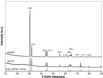
Figure 9. DSC thermographs of AAO60 and AAO15 samples: the melting temperature reduces slightly with the reduction of nanowire diameter. 10 20 30 40 50 60 70 80 90 2 theta (degrees) Intensity (a.u) (200) (101) (220) (211) (301) (112) (400) (321) (420 (411)(312) AAO60 AAO15 -Sn (JCPDF, 4-673)
Figure 10. XRD patterns of large-scale AAO/Sn nanowire composite for the AAO15 and AAO60 samples, and the position and relative intensities of polycrystallineβ-Sn (JCPDF, 4-673). Marked above individual peaks are Miller indices corresponding to lattice planes of polycrystallineβ-Sn.
XRD experiment was performed on the bottom face of the AAO/nanowire composite after removing the Al and barrier layer as described in section3.2. The XRD patterns, as shown in figure10, were indexed to the body-centred-tetragonal (bct)
β-Sn structure with lattice constants a = b = 5.82 Å;
c = 3.17 Å. All the observed peaks, both for the AAO60
and AAO15 samples, were found to match very closely to the standard polycrystalline β-Sn (JCPDF, 4-673). For the AAO60 sample, the intensity for (200) was almost 4.0 times higher than that of the secondary peak (101). This is higher than expected as the ratio of the intensities of (200) and (101) for polycrystalline β-Sn is 1.1. On the other hand, for the AAO15 sample, the relative intensities of the peaks were very similar to that from the standard polycrystallineβ-Sn with no preferred orientation. The reason for this in not clear yet, but further investigation is underway.
A transmission electron microscope (TEM) was employed to further study the morphology, crystallinity and growth orientation of individual nanowires that were deposited on a Cu
100 nm [021] (200) (112) [100] 100 nm 100 nm [021] (200) (112) [100]
Figure 11. TEM micrograph of a randomly selected single nanowire. The black circles indicate the areas from which the electron diffraction pattern (ED) was taken. Note that the ED patterns remain the same along the wire length. The zone axis in this case was [021] and the growth direction is [100].
grid after the AAO template was thoroughly dissolved. TEM micrographs taken from various randomly selected∼60 nm diameter Sn nanowires revealed that the nanowires were dense, continuous, and uniform in diameter along the length of the nanowire. A typical TEM micrograph of a randomly selected individual nanowire is shown in figure11. Although it was clearly shown from the cross section of the Sn-filled AAO template (figure6) that the nanowires had the same length as the thickness of the AAO template (10µm), TEM observation revealed that the majority of the freestanding nanowires were less than 5 µm in length when liberated from the AAO template. The nanowires might have been broken to form shorter nanowires as a result of the vigorous sonication and centrifugation steps in the nanowire separation procedure. Selected-area electron diffraction (SAED) patterns taken along the length of a 60 nm diameter nanowire showed the same single set of ED patterns along the length of the wire, verifying single crystallinity of the nanowires. After analysing several SAED patterns from randomly selected nanowires, it was concluded that although other directions were observed, the growth direction for the majority of the wires was along [100]. This is basically in good agreement with results reported previously [4] where it was found that the majority of the Sn nanowires synthesized by electrochemical deposition also had preferred [100] growth direction.
From the XRD and TEM observations, it can be deduced that the nanowires in the AAO60 sample are predominantly oriented along the [100] direction. In addition, from the current results and earlier reported results [4] it appears that regardless of the fabrication process [100] may be the preferred growth direction for Sn nanowires in the 40–160 nm diameter range.
4. Summary
Sn nanowires with 15 and 60 nm in diameter were successfully fabricated by injecting molten Sn into the nanochannels of an AAO template by applying hydraulic pressure. A filling ratio close to 100% was achieved by drying (at 450◦C) and
C-C Chen et al
degassing the template for a short period of time before injection. Increasing the injection pressure above the estimated value also helped in improving the filling ratio. A methodology was developed for a controlled partial removal of the AAO template in order to partially expose nanowires. SEM and TEM examination of the Sn nanowires showed that the nanowires were dense and continuous, with uniform wire diameter along their entire length. Structural characterization on the 60 nm diameter Sn nanowire arrays and freestanding nanowires through XRD and using a TEM revealed that the nanowires are highly oriented along the [100] direction. DSC results showed that the melting point decreased with the decrease of the nanowire diameter.
In conclusion, we have shown that the hydraulic pressure injection method is a simple, quick, high-yield and cost-effective nanowire fabrication process. Nonetheless, the resulting Sn nanowires were of similar quality compared to the Sn nanowires fabricated by the gas pressure injection process and the electrochemical method mentioned earlier. With the hydraulic pressure injection method, one can easily apply pressure levels as high as 2 kbar, the maximum limit for the present apparatus, for injecting smaller diameter nanochannels with less difficulty provided the AAO template and Al substrate can withstand that high a pressure. The major limitation of this method arises mainly due to the Al substrate, whose melting temperature is 660◦C. Although the AAO template is stable up to 800◦C, the Al substrate that should remain attached to the AAO template during the injection process would not stand temperatures higher than its melting temperature. However, this fabrication process can be readily extended to low-melting point (<650◦C) metals as well as alloys with stoichiometric composition.
Acknowledgments
This work was supported by the Texas Institute for Intelligent Bio-Nano Materials and Structures for Aerospace Vehicles (TiiMS) funded by NASA Cooperative Agreement No. NCC-1-02038, and the National Science Council (NSC92-2216-E009-019) in Taiwan. In addition, Y Bisrat would like to thank Dr B Nattamai for valuable discussions and help with XRD analysis and C-C Chen would like to thank Dr Sze-Shun Wong of Lynntech, Inc. for the helpful information on the post-treatment of the sample. Finally, the authors would like to acknowledge the efforts of Dr D Davis in facilitating the research collaboration between Taiwan and TiiMS.
References
[1] Wang X F, Zhang L D, Zhang J, Shi H Z, Peng X S, Zheng M J, Fang J, Chen J L and Gao B J 2001 J. Phys. D: Appl. Phys.34 418
[2] Heng Yu, Gibbons P C and Buhro W E 2004 J. Mater. Chem. 14 595
[3] Hirata T, Satake N, Jeong G-H, Kato T, Hatakeyama R, Motomiya K and Tohji K 2003 Appl. Phys. Lett.83 1119 [4] Tian M, Wang J, Snyder J, Kurtz J, Liu Y, Schiffer P,
Mallouk T E and Chan M H W 2003 Appl. Phys. Lett. 83 1620
[5] Jo S H, Lao J Y, Ren Z F, Farrer R A, Baldacchini T and Fourkas J T 2003 Appl. Phys. Lett.83 4821
[6] Ji C and Searson P C 2002 Appl. Phys. Lett.81 4437 [7] ParkW I, Kim D H, Jung S-W and Yi G-C 2002 Appl. Phys.
Lett.80 4232
[8] Yao B D, Chan Y F and Wang N 2002 Appl. Phys. Lett.81 757 [9] Lao J Y, Wen J G and Ren Z F 2002 Nano Lett.2 1287 [10] Banerjee D, Lao J Y, Wang D Z, Huang J Y, Ren Z F,
Steeves D, Kimball B and Sennett M 2003 Appl. Phys. Lett. 83 2061
[11] Xu C, Xu G, Liu Y and Wang G 2002 Solid State Commun. 122 175
[12] Liu Z Q and Pan Z W 2000 J. Phys. Chem. Solids61 1171 [13] Barsoum M W, Hoffman E N, Doherty R D, Gupta S and
Zavaliangos A 2004 Phys. Rev. Lett.93 206104 [14] Chen Y, Cui X, Zhang K, Pan D, Zhang S, Wang B and
Hou J G 2003 Chem. Phys. Lett.369 16
[15] Furuta N and Hamamura K 1969 Japan. J. Appl. Phys.8 1404 [16] Ma X L, Li Y and Zhu Y L 2003 Chem. Phys. Lett.376 794 [17] Ying Z, Wan Q, Song Z T and Feng S L 2004 Nanotechnology
15 1682
[18] Arutyumov K Y, Ryynanen T V and Pekola J P 2001 Phys. Rev. B63 092506
[19] Michotte S, Matefi-Tempfli S and Piraux L 2003 Appl. Phys. Lett.82 4119
[20] Kolmakov A, Zhang Y, Cheng G and Moskovits M 2003 Adv. Mater.15 997
[21] Zhang J, Wang X, Peng X and Zhang L 2002 Appl. Phys. A 75 485
[22] Yang S G, Zhu H, Yu D L, Jin Z Q, Tang S L and Du Y W 2000 J. Magn. Magn. Mater.222 97
[23] Yin A J, Li J, Jian W, Bennet A J and Xu J M 2001 Appl. Phys. Lett.79 1039
[24] Huber C A, Huber T E, Sadoqi M, Lubin J A, Manalis S and Prater C B 1994 Science 263 800
[25] Zhang Z, Ying J Y and Mildred S J 1998 J. Mater. Res. 13 1745
[26] Zhang Z, Gekhtman D, Dresselhaus M S and Ying J Y 1999 Chem. Mater.11 1659
[27] Chen C C, Chen J H and Chao C G 2005 Japan. J. Appl. Phys. 44 1529
[28] Chen C C, Kuo C G and Chao C G 2005 Japan. J. Appl. Phys. 44 1524
[29] Brandes A 1983 Semithells Metals Reference Book (New York: Butterworth & Co) pp 14–8
[30] Yuan F Z, Mukai K, Takagi K, Ohtaka M, Huang W L and Lui Q S 2002 J. Colloid Interface Sci.254 338 [31] Xu T T, Piner R D and Ruoff R S 2003 Langmuir19 1443 [32] O’Sullivan J P and Wood G C 1970 Proc. R. Soc. A 317 511 [33] Zhang Z, Li J C and Jiang Q 2000 J. Phys. D: Appl. Phys.
33 2653
[34] Sheng H W, Ren G, Peng LM, Hu Z Q and Lu K 1996 Phil. Mag. Lett.73 179
[35] Chattopadhyay K and Goswami R 1997 Prog. Mater. Sci. 42 287
[36] Allen G L, Gile W W and Jesser W A 1980 Acta. Metall. 28 1695
[37] Mardilovich P P, Govyadinov A N, Mukhurov N I,
Rzhevskii A M and Paterson R 1995 J. Membr. Sci.98 131
![Figure 2. A plot showing the estimated external pressure as a function of channel diameter from the simplified Washburn equation [ 25 ] for molten Sn assuming a contact angle of 165 ◦](https://thumb-ap.123doks.com/thumbv2/9libinfo/7627226.133840/4.892.91.436.121.353/estimated-external-pressure-function-diameter-simplified-washburn-assuming.webp)