Enhanced Light Extraction of High-Voltage Light
Emitting Diodes Using a Sidewall Chamfer
Structure
Ping-Chen Wu,1 Sin-Liang Ou,2 Ray-Hua Horng,3 Fellow, IEEE, and Dong-Sing Wuu,1
Senior Member, IEEE
1
Department of Materials Science and Engineering, National Chung Hsing University, Taichung 40227, Taiwan, R.O.C.
2
Department of Materials Science and Engineering, Da-Yeh University, Changhua 51591, Taiwan, R.O.C. 3
Institute of Electronics, National Chiao Tung University, Hsinchu 30010, Taiwan, R.O.C.
Abstract: High-voltage light-emitting diodes (HV-LEDs) were prepared with 4 × 2 microcells. A novel technique for enhancing the light extraction of HV-LEDs by using wet-etched chamfer structures in the sidewalls of each cell is proposed. The thicknesses of the u-GaN layers used were in the range of 3–7 μm. Simulations revealed that the light extraction of the HV-LEDs with chamfer structures would be enhanced by increasing the u-GaN thickness. The output power (@80 mA) of the HV-LEDs without chamfer structures was 538.0–539.1 mW. However, the output powers (@80 mA) of the HV-LEDs with chamfer structures and u-GaN thicknesses of 3, 5, and 7 μm were increased to 555.3, 573.1, and 561.6 mW, respectively. The 7 μm thick u-GaN layer led to an extremely large thickness of the HV-LED epitaxial structure, which caused difficulties during the wet etching process. Because of the apparent decrease in the wet etching rate of GaN, the damages to the epitaxial structures of the HV-LED with the 7 μm thick u-GaN was more obvious. Therefore, the device’s light extraction was slightly reduced. The results confirm that chamfer structures are highly useful for improving the performance of HV-LEDs, especially for the u-GaN thickness of 5 μm.
Index Terms: High-voltage light emitting diodes, sidewall chamfer structure, wet etching, Trace-Pro simulation, light extraction.
1. Introduction
Nitride-based semiconductors consisting of GaN, InGaN, or AlGaN have recently been effectively developed for use in short-wavelength light-emitting diodes (LEDs). Because of their excellent optoelectronic performance, these nitride-based LEDs have numerous potential applications including traffic signals, solid-state lighting, and back lighting in liquid crystal displays [1]–[3]. For these applications, high-power LEDs with a large chip size are required. However, a severe problem associated with large chips is efficiency droop, which is caused by poor current spreading when LEDs are operated at a high injection current [4], [5]. To overcome this problem, multiple micro-LEDs on large-area chips have been designed. Self-rectified alternating-current LEDs were then presented that properly connected these micro-LEDs. However, using alternating-current LEDs leads to relatively low output power, equal to only half that generated from the active region. Favorably, this issue can be solved by fabricating series-connected micro-LEDs on a large-area chip. This technique ensures that a single LED connected with several microcells can be driven with a high voltage (>20 V) and a low direct current (<100 mA). Series-connected micro-LEDs are called high-voltage LEDs (HV-LEDs) [6]–[11]. In comparison to conventional LEDs, HV-LEDs possess a more favorable current-spreading effect, a relatively low injection current, a high forward-voltage operation, and a greater reliability under an identical output power.
This article has been accepted for publication in a future issue of this journal, but has not been fully edited. Content may change prior to final publication. Citation information: DOI 10.1109/JPHOT.2017.2710019, IEEE Photonics Journal
sidewalls of LEDs were often used [12]–[15]. However, up to now, there is no research on the sidewall etching process applied for the HV-LEDs. In the current study, the light extraction of GaN-based HV-LEDs was improved using a novel technique involving the preparation of chamfer structures in the sidewalls of the epitaxial structure of each microcell. The optoelectronic performance of HV-LEDs with and without chamfer structures was investigated in detail. Devices with different thicknesses of epitaxial structure were also studied by increasing the thickness of the undoped GaN (u-GaN) layer from 3 to 7 μm. For the chamfer structures in the HV-LEDs (with various u-GaN thicknesses), the angles of approximately 40° between GaN and sapphire were formed. These devices were fabricated for the measurements of optoelectronic performance.
2. Experimental Details
In this study, epitaxial structures of GaN-based LEDs were grown on triangle-shaped patterned sapphire substrates (PSSs) by using metalorganic chemical vapor deposition. To avoid the loss of light through the substrate, three pairs of TiO2/SiO2 distributed Bragg reflectors were deposited on the underside of the sapphire substrate. The epitaxial structure deposited on the top of the substrate consisted of a u-GaN layer (3–7 μm), Si-doped n-type GaN layer (3 μm), InGaN/GaN multiple quantum wells (150 nm), and a Mg-doped p-type GaN layer (150 nm). The thicknesses used for the u-GaN layer were 3, 5, and 7 μm. Each microcell LED used for realizing the HV-LED had a size of 0.254 mm × 0.254 mm and was formed through standard photolithography and etching processes. The HV-LED was constructed by series-connecting 4 × 2 microcells, and a SiO2 layer was employed as a passivation layer to flatten the trenches between cell chips. Ti/Al/Ti/Au (thicknesses: 20/1500/20/200 nm) metal multilayer grown using e-beam evaporation served as the electrode and reflective mirror of the device. HV-LEDs were fabricated through the connection of eight cells that had 3, 5, or 7 μm thick u-GaN layers. Half of the fabricated devices had chamfer structures in the sidewalls of each cell. Thus, six types of HV-LED are presented in this paper. The HV-LED had a size of 0.5588 mm × 1.1176 mm. The chamfer structures in the sidewalls of the epitaxial structure of each microcell were fabricated as illustrated in Fig. 1. First, isolation etching by using an inductively coupled plasma–reactive ion etching (ICP-RIE) system was used to etch the epitaxial structures between cells until the triangle-shaped PSS was exposed [Fig. 1(a)]. Next, a 2.5 μm thick SiO2 layer was grown using plasma-enhanced chemical vapor deposition (PECVD), and this layer was employed as the etching stop layer for the sidewall etching of each cell [Fig. 1(b)]. The SiO2 layer deposited at the bottom of the trench was then removed using ICP-RIE [Fig. 1(c)]. Subsequently, the residual u-GaN layer at the bottom of the trench was removed by soaking the LED chips in H2SO4:H3PO4 (3:1) solution at 85 °C. Chamfer structures were then fabricated in the sidewalls of the epitaxial structure of each cell [Fig. 1(d)]. Finally, the residual SiO2 on the top and sidewall of the epitaxial structure was cleaned using ICP-RIE, and the LED cell with chamfer structures in the sidewalls was prepared [Fig. 1(e)].
For each device, we have prepared twenty samples to analyze the electrical characteristics and optoelectronic performance. In this study, the optoelectronic performance of HV-LEDs with and without chamfer structures in the sidewalls of each microcell was characterized. The cross-sectional morphology of the LED cells was determined using scanning electron microscopy (SEM). The light emission of the HV-LEDs was investigated using a near-field optical microscope (Spiricon, FX-50) combined with a charge-coupled device. The current–voltage (I–V) characteristics of the HV-LEDs were analyzed using a semiconductor parameter analyzer (Keithley 2400 sourcemeter), and the output power performance was measured using a calibrated integrating sphere. Trace-Pro software (commercial light-simulation software based on geometrical optics) was used to simulate the photon trajectories of LEDs.
Fig. 1. Fabrication processes for chamfer structures in the sidewalls of epitaxial structure of each microcell: (a) Separation for every cell via the isolation etching, (b) deposition of the etching stop layer (SiO2) by PECVD, (c) removal
of the SiO2 layer deposited on the bottom of the trench via ICP-RIE technique, (d) formation of chamfer structures in
the sidewalls of each cell through the wet etching method, and (e) cleaning of the residual SiO2 on the top and the
sidewalls of epitaxial structure by ICP-RIE.
3. Results and Discussion
Cross-sectional SEM images illustrate the differences in the device structure of HV-LEDs fabricated with and without chamfer structures in the microcell sidewalls (Fig. 2). As mentioned, the SiO2 layer grown using PECVD acted as the etching stop layer. Fig. 2(a) shows an SEM image of the SiO2 layer deposited on the LED epitaxial structure. Subsequently, the SiO2 layer at the bottom of the trench between cells was removed using dry etching, and the corresponding SEM image is presented in Fig. 2(b). Through wet etching using 85 °C-heated H2SO4:H3PO4 solution, the chamfer structures were then formed in the sidewalls of the LED cells [Fig. 2(c)]. Fig. 2(d) depicts an SEM image of the structure of the HV-LED fabricated without chamfer structures.
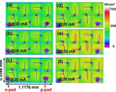
The light extraction characteristics of the HV-LEDs were investigated by analyzing surface light emission through a near-field optical microscope. Figs. 3(a)–3(c) and 3(d)–3(f) present the surface light emission patterns (@20 mA) of the HV-LEDs without and with chamfer structures in the sidewalls of each cell, respectively. The near-field microscope was equipped with a video analyzer (Beam-View Analyzer, Coherent) connected to a computer. As illustrated in Figs. 3(a)–3(c), the intensity of light emission around the trench region was lower than that around the center of each LED cell. This indicates that the light extraction through the trench of the HV-LEDs without chamfer structures in the cell sidewalls was weak, which could decrease their emission performance. As shown in Figs. 3(d)–3(f), the HV-LEDs prepared with chamfer structures in the cell sidewalls had saturated light extraction in the trench region. Therefore, the near-field optical measurements reveal that the light extraction of HV-LEDs can be improved efficiently by forming chamfer structures in the sidewalls of each cell.
This article has been accepted for publication in a future issue of this journal, but has not been fully edited. Content may change prior to final publication. Citation information: DOI 10.1109/JPHOT.2017.2710019, IEEE Photonics Journal
Fig. 2. Cross-sectional SEM images of (a) the etching stop layer (SiO2) deposited on the HV-LED, (b) removal of the
SiO2 layer deposited on the bottom of the trench, (c) the HV-LED with chamfer structures in the sidewalls of microcell,
Fig. 3. Without forming chamfer structures in the sidewalls of each cell, the surface light emission patterns (@20 mA) of the HV-LEDs with (a) 3 μm thick, (b) 5 μm thick, and (c) 7 μm thick u-GaN layers. With forming chamfer structures in the sidewalls of each cell, the surface light emission patterns (@20 mA) of the HV-LEDs with (d) 3 μm thick, (e) 5 μm thick, and (f) 7 μm thick u-GaN layers.
The Trace-Pro simulation results are illustrated in Fig. 4. Here, the Trace-Pro simulations were used to simulate the photon trajectories of microcells (not series-connected HV-LEDs). However, it can be predicted that the trend of simulation results for these microcells is similar to that for the HV-LEDs. In the simulations, 60-mW power (10,000 photons) was set to emit randomly from the multiple quantum well (MQW) active region. After performing the simulations on the microcells without chamfer structures in the cell sidewalls (u-GaN thickness: 3–7 μm), we found that the simulation results of these three microcells were the same to each other. This indicates that the simulation result of the microcell without chamfer structures is not affected by increasing the u-GaN thickness from 3 to 7 μm. Therefore, we have added only one figure to present the simulation results of the microcells without chamfer structures (u-GaN thickness: 3–7 μm), as shown in Fig. 4(a). The numbers of output ray of the microcell without chamfer structures was 2993. Figs. 4(b), 4(c), and 4(d) present the simulation results for the microcells with chamfer structures in the cell sidewalls, where the u-GaN thicknesses in the cells were 3, 5, and 7 μm, respectively. The numbers of output rays of these three HV-LEDs were 3206, 3321, and 3393, respectively. In the simulations, the epilayer absorption and the effect of the silver cup in the epoxy lamp were not considered. Obviously, the chamfer structures formed in the sidewalls of the microcell is indeed helpful for enhancing its light extraction. Moreover, when the chamfer structures were prepared, the light extraction of LED could be improved by increasing the thickness of the u-GaN layer.
Figs. 5(a) and 5(b) illustrate the forward voltage and light output power as functions of injection current for the HV-LEDs (u-GaN thickness: 3–7 μm) without and with chamfer structures in the sidewalls of each cell, respectively. The injection current was increased from 0 to 80 mA. At injection currents of 20, 40, 60, and 80 mA, the forward voltages of the HV-LEDs without chamfer structures were determined to be 24.3, 26.1, 27.5, and 28.6 V, respectively [Fig. 5(a)]. When the injection current was increased similarly for the HV-LEDs with chamfer structures, the I–V characteristics were almost identical to those for the corresponding devices without chamfer structures [Fig. 5(b)]. This reveals that the I–V performance of HV-LEDs is not affected by the introduction of chamfer structures in the sidewalls of each cell. Furthermore, u-GaN thickness was discovered to have almost no effect on the output power of the HV-LEDs without chamfer structures in the cell sidewalls [Fig. 5(a)], which were measured to be 538.0–539.1 mW (@80 mA). The output power levels of the HV-LEDs with chamfer structures in the cell sidewalls were revealed to be higher compared with those of the HV-LEDs without
This article has been accepted for publication in a future issue of this journal, but has not been fully edited. Content may change prior to final publication. Citation information: DOI 10.1109/JPHOT.2017.2710019, IEEE Photonics Journal
power levels (@80 mA) of the HV-LEDs with chamfer structures were 555.3, 573.1, and 561.6 mW, respectively. Beveled sapphire was fabricated to enhance the light extraction of conventional LEDs (not for HV-LEDs) [16]. The morphology of the LED cell fabricated with chamfer structures in the sidewalls was similar to that of the device prepared on beveled sapphire, thus confirming that they both enhance the light extraction of the device. On the other hand, there were several researches about the process of sidewall etching of GaN-based LEDs for improving the device performance [12]–[15]. However, these previous works all focused on the fabrication of single-cell LEDs (not HV-LEDs). Currently, in the LED industry where stable device fabrication processes are used, the output power of HV-LEDs is improved by approximately 4%–5% per year. The present study discovered that the enhancement in output power of HV-LEDs fabricated with the novel proposed method reached 6.5%.
Fig. 4. (a) The Trace-Pro simulation taken from the microcell without forming chamfer structures in the cell sidewalls. After forming chamfer structures in the cell sidewalls, the Trace-Pro simulations taken from the microcells with (b) 3 μm thick, (c) 5 μm thick, and (d) 7 μm thick u-GaN layers.
Fig. 5. Forward voltage and light output power as functions of injection current for the HV-LEDs (a) without and (b) with chamfer structures in the sidewalls of each cell. The error bars represent the variations of forward voltage and output power as determined from twenty samples.
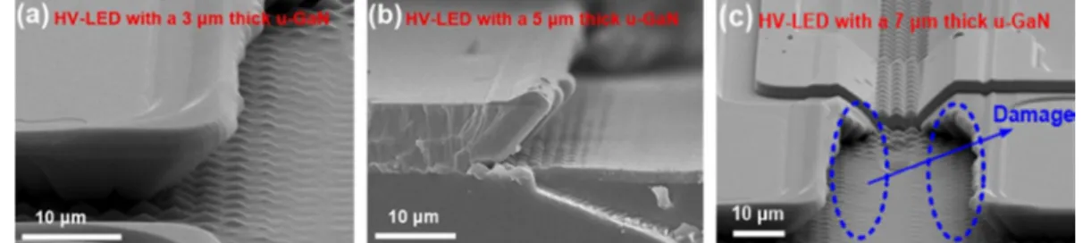
Notably, the largest improvement in output power was observed in the HV-LED with the 5 μm thick u-GaN layer, not that with the 7 μm thick u-GaN layer; this does not agree with the simulation results (Fig. 4). SEM was performed to explain this difference. Figs. 6(a), 6(b), and 6(c) show the SEM images of the HV-LEDs with chamfer structures and u-GaN thicknesses of 3, 5, and 7 μm, respectively. In these three images, the wet etching durations were kept at 15 min. The chamfer structures in the sidewalls of the LED cells with the 3 and 5 μm thick u-GaN layers were more complete [Figs. 6(a) and 6(b)]. When the 7 μm thick u-GaN layer was used, the full epitaxial structure was associated with an extremely large thickness of nearly 11 μm. This caused difficulties during the wet etching process, and the optimal chamfer structures are hard to form, as shown in Fig. 6(c). Actually, as the u-GaN thickness was increased, the wet etching rate of GaN decreased gradually. This was attributed that more and more reaction products formed during the etching process, obstructing the etching channels and hindering the reaction between GaN and the etching solution. However, based on our observation, when the u-GaN thickness was increased to 7 μm, the decrement in the wet etching rate of GaN became much obvious and the prepared chamfer structures were nonobvious if the etching time was insufficient. It can be speculated that the u-GaN thickness of 7 μm in our HV-LED device is critical for the wet etching process. As shown in Figs. 6(a) and 6(b), the chamfer structures were extended from u-GaN to p-GaN. In other words, there were slight damages to the epitaxial structures (MQW and p-GaN) of the HV-LEDs with the 3 and 5 μm thick u-GaN layers during the wet etching process. Nevertheless, due to the obvious decrement in the wet etching rate of GaN, the damages to the epitaxial structures of the HV-LED with the 7 μm thick u-GaN layer was more obvious, as marked by blue circles in Fig. 6(c). This would lead to a slight reduction in the emitting area of this HV-LED. It should be noted that the optimal etching durations of these three HV-LEDs for optoelectronic measurements (Fig. 5) were approximately 18, 23, and 30 min, respectively. Although the optimal optoelectronic performance of the HV-LED with the 7 μm thick u-GaN can be achieved after wet etching for 30 min, the chamfer structure in this device is still not complete. Additionally, the reduction of the emitting area also occurred in this device. Therefore, the device with the 7 μm thick u-GaN layer did not demonstrate the highest improvement in output power when it had chamfer structures. Even though the incomplete chamfer structures and a slight reduction of emitting area occurred in the HV-LED with the 7 μm thick u-GaN layer after the wet etching process for 30 min, the light output performance was still better than that without the chamfer structures (Fig. 5). This can confirm again that the chamfer structures indeed play an important role in enhancing the light extraction. In fact, because of the formation of chamfer structures, it can reduce the total internal reflection and more light rays can be easily emitted from the sidewalls. Extending the wet etching time (> 30 min) during the fabrication of the HV-LED with the 7 μm thick u-GaN can obtain more complete chamfer structures, however, the problem of overetching would be engendered, resulting in the severer damages in the epilayers and the more reduction in the emitting area.
Fig. 6. After forming chamfer structures, the SEM images of the HV-LEDs with (a) 3 μm thick, (b) 5 μm thick, and (c) 7 μm thick u-GaN layers. In these three images, the wet etching durations were kept at 15 min.
Fig. 7 shows the schematics of HV-LEDs with various u-GaN thicknesses (3–7 μm) after wet etching for 15 min. For the device with the u-GaN thickness of either 3 or 5 μm, chamfer structures were more completely formed in the sidewalls of each LED cell [Fig. 7(a)]. However,
This article has been accepted for publication in a future issue of this journal, but has not been fully edited. Content may change prior to final publication. Citation information: DOI 10.1109/JPHOT.2017.2710019, IEEE Photonics Journal
obviously and the prepared chamfer structures were incomplete [Fig. 7(b)]. In these samples, the chamfer structures were all extended from u-GaN to p-GaN. However, because the wet etching rate of GaN in the HV-LED with the 7 μm thick u-GaN layer became much slow, the damages to the epitaxial structures of this sample were more apparent, causing the reduction in the emitting area.
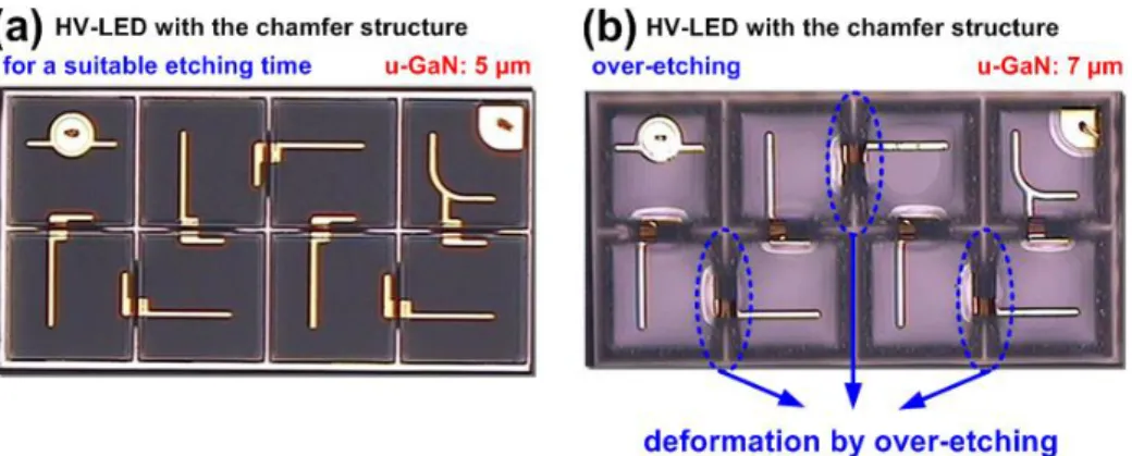
Optical microscopy (OM) was also used to determine the morphology of the HV-LEDs prepared with chamfer structures in the sidewalls of each cell. Fig. 8(a) depicts an OM image of the HV-LED with the 5 μm thick u-GaN layer after wet etching for a suitable etching duration (23 min), demonstrating that almost no deformation was generated in the sidewalls of the microcells. Fig. 8(b) presents an OM image of the HV-LED with the 7 μm thick u-GaN layer and more complete chamfer structures that had been overetched (> 30 min). Several severely damaged epitaxial structures could be observed in the cell sidewalls, which led to deformations, as marked by blue circles in the figure. This damage would cause a short-circuit current in the HV-LED, thus degrading the optoelectronic performance of this device.
Fig. 7. Mechanisms of wet etching processes for 15 min performed on the epitaxial structures of (a) HV-LED with the 3 or 5 μm thick u-GaN layer and (b) HV-LED with the 7 μm thick u-GaN layer.
Fig. 8. OM images of (a) HV-LED with the 5 μm thick u-GaN layer after wet etching for a suitable etching duration and (b) HV-LED with the 7 μm thick u-GaN layer through the overetching process.
4. Conclusions
This study presents GaN-based HV-LEDs connected with 4 × 2 microcells. Introducing chamfer structures in the sidewalls of each cell efficiently improved the light extraction of the HV-LEDs. Trace-Pro simulation results reveal that the light extraction of the HV-LEDs with chamfer structures could be further enhanced if the u-GaN thickness was increased from 3 to 7 μm. The output power levels (@80 mA) of the HV-LEDs without chamfer structures (u-GaN thickness = 3–7 μm) were in the range of 538.0–539.1 mW. The output power levels (@80 mA) of the HV-LEDs with chamfer structures, however, were 555.3, 573.1, and 561.6 mW for the 3, 5, and 7 μm thick u-GaN layers, respectively. Thus, the HV-LED with the 5 μm thick u-GaN layer had the highest improvement in output power after the introduction of chamfer structures in the sidewalls of each cell. This disagreed with the simulation results, which predicted the optimal
enhancement for the HV-LED with the 7 μm thick u-GaN layer. However, the wet etching rate was obviously decreased when the 7 μm thick u-GaN layer was used, which resulted in incomplete chamfer structures, the apparent damages to the epitaxial structure, and the reduction of emitting area. Consequently, the enhancement in light extraction of the HV-LED with the 7 μm thick u-GaN layer was slightly reduced. These results thus reveal that the formation of chamfer structures in the sidewalls of each cell can facilitate the process of enhancing the performance of HV-LEDs, particularly for an epitaxial structure with a 5 μm thick u-GaN layer.
Acknowledgements
This work was supported by the Ministry of Science and Technology (Taiwan, R.O.C.) under Grant Nos. 104-2221-E-005-036-MY3 and 102-2221-E-005-072-MY3.
References
[1] T. Wei, L. Zhang, X. Ji, J. Wang, Z. Huo, B. Sun, Q. Hu, X. Wei, R. Duan, L. Zhao, Y. Zeng, and J. Li, “Investigation of efficiency and droop behavior comparison for InGaN/GaN super wide-well light emitting diodes grown on different substrates,” IEEE Photon. J., vol. 6, no. 6, Dec. 2014, Art. ID. 8200610.
[2]X. Bao, P. Sun, S. Liu, C. Ye, S. Li, and J. Kang, “Performance Improvements for AlGaN-based deep ultraviolet light-emitting diodes with the p-type and thickened last quantum barrier,” IEEE Photon. J., vol. 7, no. 1, Feb. 2015, Art. ID. 1400110.
[3] S. H. Park and Y. T. Moon, “Temperature droop characteristics of internal efficiency in InxGa1-xN/GaN quantum
well light-emitting diodes,” IEEE Photon. J., vol. 6, no. 5, Oct. 2014, Art. ID. 1600209.
[4] I. A. Pope, P. M. Smowton, P. Blood, J. D. Thomson, M. J. Kappers, and C. J. Humphreys, “Carrier leakage in InGaN quantum well light-emitting diodes emitting at 480 nm,” Appl. Phys. Lett., vol. 82, no. 17, pp. 2755–2757, April 2003.
[5] K. J. Vampola, M. Iza, S. Keller, S. P. DenBaars, and S. Nakamura, “Measurement of electron overflow in 450 nm InGaN light-emitting diode structures,” Appl. Phys. Lett., vol. 94, no. 6, pp. 061116-1–061116-3, Feb. 2009. [6] C. H. Tien, K. Y. Chen, C. P. Hsu, and R. H. Horng “Enhanced light output power of thin film GaN-based high
voltage light-emitting diodes,” Opt. Exp., vol. 22, no. S6, pp. A1462-A1468, Sep. 2014.
[7] W. Wang, Y. Cai, W. Huang, H. O. Li, and B. S. Zhang, “Electrical and optical properties of a high-voltage large area blue light-emitting diode,” Jpn. J. Appl. Phys., vol. 52, pp. 08JG08-1–08JG08-4, May 2013.
[8] S. J. Chang, C. Y. Chang, C. L. Tseng, C. S. Shen, and B. Y. Chen, “Failure mechanism for GaN-based high-voltage light-emitting diodes,” IEEE Photon. Technol. Lett., vol. 26, no. 11, pp. 1073–1076, Jun. 2014. [9] C. H. Wang, D. W. Lin, C. Y. Lee, M. A. Tsai, G. L. Chen, H. T. Kuo, W. H. Hsu, H. C. Kuo, T. C. Lu, S. C. Wang,
and G. C. Chi, “Efficiency and droop improvement in GaN-based high-voltage light-emitting diodes,” IEEE Electron Dev. Lett., vol. 32, no. 8, pp. 1098–1100, Aug. 2011.
[10] H. Ye, X. Chen, H. van Zeijl, A. W. J. Gielen, and G. Zhang, “Thermal transient effect and improved junction temperature measurement method in high-voltage light-emitting diodes,” IEEE Electron Dev. Lett., vol. 34, no. 9, pp. 1172–1174, Sep. 2013.
[11] R. H. Horng, K. C. Shen, Y. W. Kuo, and D. S. Wuu, “Effects of Cell Distance on the Performance of GaN High-Voltage Light Emitting Diodes,” ECS Solid State Lett., vol. 1, no. 5, pp. R21–R23, Aug. 2012.
[12] R. M. Lin and J. C. Li, “Side Wall Wet Etching Improves the Efficiency of Gallium Nitride Light Emitting Diodes,” J. Electrochem. Soc., vol. 159, no. 4, pp. H433–H439, Feb. 2012.
[13] C. M. Lin, C. F. Lin, B. C. Shieh, T. Y. Yu, S. H. Chen, P. H. Tsai, K. T. Chen, J. J. Dai, and T. L. Tsai, “InGaN-Based Light-Emitting Diodes With a Sawtooth-Shaped Sidewall on Sapphire Substrate,” IEEE Photon. Tech. Lett., vol. 24, no. 13, pp. 1133–1135, Jul. 2012.
[14] Y. Zhang, E. Guo, Z. Li, T. Wei, J. Li, X. Yi, and G. Wang, “Light Extraction Efficiency Improvement by Curved GaN Sidewalls in InGaN-Based Light-Emitting Diodes,” IEEE Photon. Tech. Lett., vol. 24, no. 4, pp. 243–245, Feb. 2012.
[15] C. F. Tsai, Y. K. Su, and C. L. Lin, “Further Improvement in the Light Output Power of InGaN-Based Light Emitting Diodes by Patterned Sapphire Substrate with KOH Wet-Chemical Etching on Sidewall,” Jpn. J. Appl. Phys., vol. 51, no. 1S, pp. 01AG04-1–01AG04-4, Jan. 2012.
[16] R. H. Horng, H. L. Hu, S. L. Ou, R. C. Lin, and C. P. Hsu, “Enhancement of light extraction for InGaN LEDs by means of beveled sapphire and cup-shaped copper sheeting,” IEEE Photon. Tech. Lett., vol. 24, no. 16, pp. 1421–1423, Aug. 2012.