Effects of growth interruption time on InGaN/GaN quantum dots
grown by metal organic chemical vapor deposition
H. H. Yao, G. S. Huang, T. C. Lu, C. Y. Chen, W. D. Liang, H. C. Kuo and S. C. Wang*
Department of Photonics and Institute of Electro-optical Engineering, National Chiao-Tung
University, Hsinchu, Taiwan, R. O. C,
ABSTRACT
Wide-bandgap gallium nitride (GaN) quantum dot (QD) structure is attractive because it is a zero-dimensional (0-D) confinement structure and has many unique physical characteristics. We have successfully grown self-assembled InGaN QDs structure by metal organic chemical vapor deposition. A high quality GaN/sapphire template with a flat surface and the suitable growth condition including low growth temperature and low V/III ratio were used to grow InGaN QDs structure. The density of InGaN QDs is about 4.5 × 1010 cm-2 with an average lateral size of 11.5 nm and an average
height of 1.6 nm. The effect of the interruption growth for InGaN QDs structure was systematic studied with the growth temperature of 660oC. The surface morphology and optical property was measured by atomic forced microscopy and
various temperature PL, respectively. The results indicated that as increasing interruption time from 30s to 120s, QDs area occupied on the surface above the wetting layer increases from 5.2% to 7.2%, and the In composition decreases from 25% to 21%. The results were discussed by considering the influences of ad-atom desorption and diffusion effect between wetting layer and InGaN QDs structure. Our results suggest that the interruption growth during an optimum time can modify the size of InGaN QDs and extend the emission wavelength to short wavelength, and at the same time improve the QD optical quality. Using this technique was feasible for formation of multi layer InGaN QDs structures and applicable for the fabrication of GaN-based light emitting devices.
Keywords: Self-assembled quantum dots, InGaN/GaN, interruption growth, MOCVD, AFM, PL
1. INTRODUCTION
GaN-based semiconductors have attracted great attentions for applications not only in light sources of short wavelength, but also high-speed/high-power electron devices. Short wavelength light emitters are required for full color display, laser printers, high density information storage, and under water communication. High temperature and high power transistors are needed for automobile engines, future advanced power distribution systems, all electric vehicles, and avionics. Actually, III-nitrides are particularly suitable for applications in these areas based on their unique properties including wide bandgap (~0.9-6.1eV), high bond energy (~2.3eV), high-saturation velocity (~2.7 x 104 cm/s),
high-breakdown field (~2 x 10⁶ V/cm), and strong excitonic effects (> 50 meV). Furthermore, Wurtzite III-nitrides
exhibit large effect of spontaneous and strain induced polarization from the noncentrosymmetric and uniaxial crystals and the piezoelectric coefficients are almost an order of magnitude larger than traditional III-V compounds such as GaAs. The very strong internal electric field induced by the polarization charge and piezoelectricity is very unique to III-nitride heterostructures and has a dramatic effect on the properties of quantum confined structures.[1]
Investigations of semiconductor quantum dots (QDs) have been very extensive, particularly in the last decade. These are fuelled by unique physical phenomena and potential device applications. There have been lots of researches recently devoted to realizing the predicted potential of 0-D quantum-confined structures. Because of their unique electronic states (i.e., atomic-like discrete states with a δ-function density of states), QDs are expected to have many interesting and useful properties for optolecetronic device applications. The semiconductor laser with a QD active
Invited Paper
Gallium Nitride Materials and Devices, edited by Cole W. Litton James G. Grote, Hadis Morkoc, Anupam Madhukar, Proc. of SPIE Vol. 6121, 612102, (2006), 0277-786X/06/$15 · doi: 10.1117/12.644706
Proc. of SPIE Vol. 6121 612102-1
region promises ultra low and temperature independent threshold current, high-frequency modulation with negligible chirping effect, and nonlinear gain effect. For GaN-based light device, the application of QD structure in laser diodes (LDs) is expected to have lower threshold currents due to the enhancement of excitonic effects in the quantum dots [2]. On the other hand, III-nitride QD structures can reduce the effect of defect density which was generated due to the use of foreign substrate with large lattice mismatch [3]. Therefore, QD structure is important to develop low threshold GaN-based LDs, which are generally known by the difficulties of the reduction of the threshold current density in GaN GaN-based materials due to the large effective mass in comparison with GaAs or InP based materials.
Recently, researches of InGaN QDs structure grown by metal-organic chemical vapor deposition (MOCVD) have been reported. The self-assembled InGaN QDs was first reported by using anti-surfactant to change the surface free energy of epi-layers [4]. Si as the anti-surfactant was used to form the InGaN QDs in the InGaN/AlGaN system. The self-assembled InGaN QDs without using anti-surfactant were also reported [5]. However, the mechanism of formation of these QDs due to the strain-induced mode or phase separation is not fully understood yet. The characteristics of these InGaN QDs can be controlled by deposition thickness, and growth temperature. In addition, interruption growth time, which is the time of between the end of deposition and the capping of the quantum dot layer with barrier material, is another important factor to grow semiconductor QDs. It is believed that the interruption growth facilitates the elastic relaxation resulting from the formation of the 3D island formation, and the adatoms can relax to energetically favorable position and approach thermodynamic equilibrium [6]. For this reason, a growth interruption during the transition from two-dimensional growth can improve the quality of the quantum dot layer considerably [7]. Recently, there have been reported to grow III-nitride QD structures with interruption growth step [8, 9]. However, there are few systematic studies on the effect of interruption time for InGaN QDs. In this paper, we have successfully grown self-assembled InGaN QDs with interruption growth. The effect of interruption time on InGaN QDs has been studied. The influences of adatom desorption and diffusion on the morphological and optical properties of the InGaN QDs were investigated.
2. EXPERIMENT
All samples were grown using a low-pressure vertical-type MOCVD system (EMCORE D75). A 30 nm GaN nucleation layer were grown first at 500°C on a (0001)-oriented sapphire substrate followed by a GaN buffer layer under H2 ambient gas grown at 1110°C. During the growth of a GaN buffer layer, the flow rate of trimethylgallium
(TMG) was 68.4 mol/min and NH3 was used as a group V source with a flow rate of 3 l/min, corresponding to a
V/III ratio of about 2000. After the GaN buffer layer was grown, the growth temperature was reduced to 660°C to grow an InGaN layer, and N2 was used as the ambient gas with a flow rate of 5 l/min. Contrarily to the standard InGaN
quantum well growth, the growth temperature was reduced to facilitate the InGaN quantum dot growth [5]. During the growth of InGaN, the flow rates of TMG and trimethylindium were 4.92 and 4.80 mol/min, respectively and the flow rate of NH3 was 2 l/min, corresponding to a low V/III ratio of about 8300 in comparisons to the normal V/III ratio of
30000 in the InGaN quantum well growth. Various growth time of InGaN have been grown, and the optima growth time was determined as 30s. After the InGaN growth with growth time of 30s was completed, an interruption growth was introduced for annealing InGaN surface and the effect of interruption growth were studied by various interruption time. The surface morphologies of these samples were examined by atomic forced microscopy (AFM) and the AFM data were analyzed by Scanning Probe Image Processor (SPIP) to gather the geometric statistics of InGaN QDs. The optical characteristics of these samples were investigated by photoluminescence (PL) using a commercial microscope system.
3. RESULT AND DISCUSSION
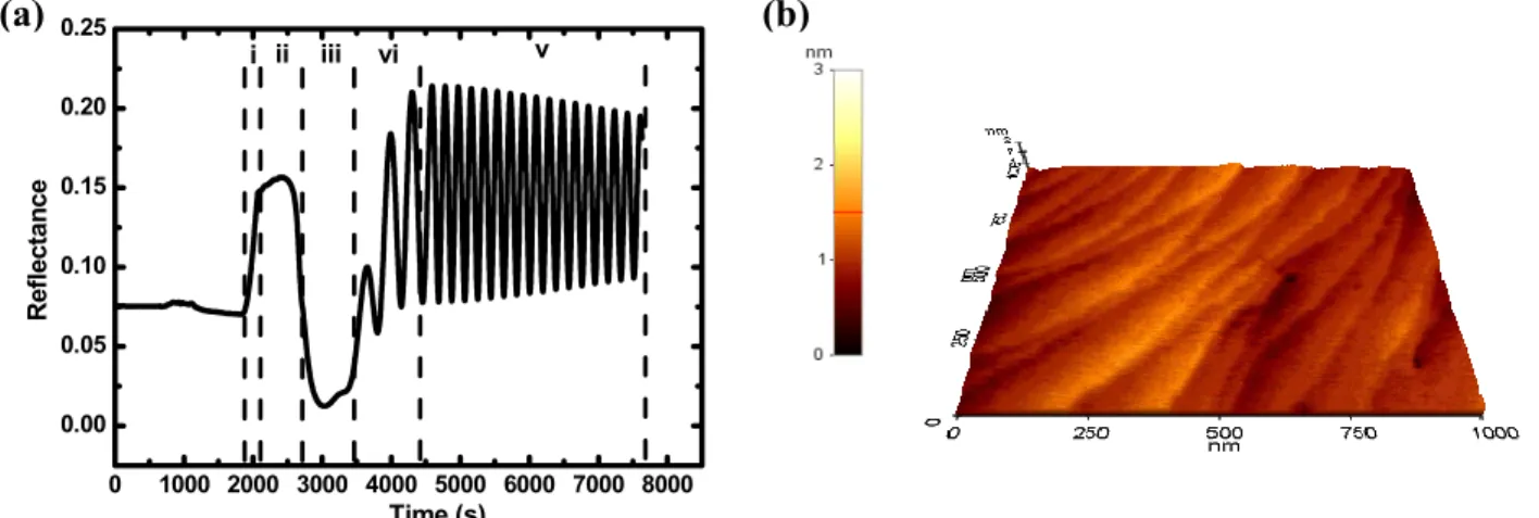
Fig.1 shows the in-situ reflectance traces and AFM image of the GaN/sapphire template. Fig. 1 (a) is the reflectance traces measured by a real-time in-situ normal-incidence optical reflectometer (λ = 600 nm). The trace of the reflectance intensity proceeded with several stages during GaN growth: (i) the nucleation layer growth, (ii) temperature ramping for high temperature undoped GaN growth, (iii) lateral growth and surface roughening, (iv) island coalescence, and (v) quasi-two-dimensional (2D) growth of undoped GaN. Fig. 1 (b) shows the AFM image of the surface morphology of the GaN/sapphire template. There are some dark spots on the surface with a density of about 3 × 108 cm -2. These dark spots are due to threading dislocation between the GaN layer and sapphire substrate. The surface of the
Proc. of SPIE Vol. 6121 612102-2
GaN/sapphire template is very flat with an average deviation Ra = 0.14 nm. Previous report had shown that the flat
template surface was important to fabricate self-assembled InGaN QDs without using anti-surfactant [5].
After the GaN layer was grown, the growth temperature was reduced to 660oC to grow the InGaN thin film.
Three samples with different growth time of the InGaN have been grown under a low V/III ratio of about 8300 in comparisons to the normal V/III ratio of 30000 in the InGaN quantum well growth. Fig. 2 shows AFM images of InGaN QDs with different growth time tg : (a) 30 s, (b) 40 s, and (c) 50 s. The topographic images of three InGaN QDs samples
were showed small islands morphology. However, there is no self-assembled InGaN QDs appeared on the surface if the growth time is smaller than 15s (not shown). Fig. 3 is the section analysis of Fig. 2(a). Fig. 3(a) is the section profile along the dash line in Fig. 2(a), and the dense QDs distribution can be observed. Fig.3(b) clearly shows the shape profile of a single InGaN QD structure with the lateral width and height of about 30 nm and 0.8 nm, respectively.
(a)
0 1000 2000 3000 4000 5000 6000 7000 8000 0.00 0.05 0.10 0.15 0.20 0.25 v vi iii ii i Ref lect an ce Time (s)Fig. 1 The in-situ reflectance traces and AFM image of the GaN/sapphire template. (a) In-situ normal reflectance measurement for a whole sequence of GaN epitaxial thin film on sapphire substrate. (b) Surface morphology of GaN/sapphire template.
(b)
Fig. 2 The surface morphologies of InGaN QDs with different growth time performed by AFM over areas of 1 µm square: (a) tg = 30s, (b) tg = 40s, and (c) tg = 50s.
Proc. of SPIE Vol. 6121 612102-3
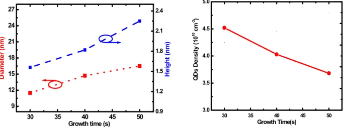
In order to analyze these AFM data and gathered the geometric statistics of InGaN QDs, we used Scanning Probe Image Processor (SPIP) to analyze the AFM data of InGaN QDs structures. The results show that the InGaN QDs size depends on the growth time of InGaN. When the growth time of InGaN was varied from 30 s to 50 s, the average diameter of InGaN QDs was increased from 11.5nm to 16.0nm, and the average height of InGaN QDs was also increased from 1.6nm to 2.3nm (Fig. 3 (a)). However, the density of InGaN QDs was decreased from 4.5 x 1010 cm-2 to
3.0 x 1010 cm-2 (Fig. 3 (b)).
Using the result of Fig. 2, the effect of interruption growth for self-assembled InGaN QDs was studied. Three samples have been grown with a fixed growth time of 30s and an interruption growth was introduced for these samples with different interruption time (tint) of 30 s, 60 s, and 120 s for sample A, B and C, respectively. Fig. 5 shows the AFM
scan results of InGaN QDs samples performed over an area of 1 m square. These AFM images show the sample surfaces with a series of variations tint of 30, 60, and 120 s, respectively. The results show that the interruption growth at
660oC could influence the morphologies of these samples. From the surface roughness analysis of AFM measurement
0 1 5 3 0 4 5 6 0 7 5 9 0 0 . 0 0 . 2 0 . 4 0 . 6 0 . 8 1 . 0 He igh t (nm) D i s t a n c e ( n m ) 0 2 0 0 4 0 0 6 0 0 8 0 0 1 0 0 0 0 . 0 0 . 2 0 . 4 0 . 6 0 . 8 1 . 0 1 . 2 1 . 4 1 . 6 Heigh t (nm) D i s t a n c e ( n m )
Fig. 3 Section analysis of Fig. 2(a). (a) The section profile along the dash line, and the dense QDs distribution can be observed. (b) The section profile of single QD structure. The clear shape profile shows single InGaN QD structure with the lateral width and height of about 30 nm and 0.8 nm, respectively.
0.9 1.2 1.5 1.8 2.1 2.4 30 35 40 45 50 9 12 15 18 21 24 27 Height ( n m) Diamet er ( n m) Growth time (s) 3.0 3.5 4.0 4.5 5.0 30 35 40 45 50 QD s D en si ty ( 10 10 cm -2 ) Growth Time(s)
Fig. 4 The geometric statistics of InGaN QDs gathered by SPIP from AFM results. (a) Average diameter and height in dependence of the growth time of InGaN, and (b) Dependence of the density on the growth time of InGaN.
Proc. of SPIE Vol. 6121 612102-4
result, the surface roughness of average deviation decrease from Ra=0.26nm to Ra=0.21nm by increasing tint from 30s to
120s.
Fig. 6(a) shows the averaged height and diameter of the samples with various interruption times. The mean size (diameter, height) of sample A is (14nm, 2.4nm), and sample B is decreased to (11.5nm, 1.6nm), and then sample C is increased to (15nm, 2.5nm). Fig. 6(b) shows the dependence of the coverage, which describes how much QDs areas occupied on the surface above the wetting layer, and QDs density on the interruption time. The coverage increases from 5.2% to 7.2% by increasing tint from 30s to 120s. On the other hand, the QDs densities are 2.88 * 1010 cm-2, 4.5 * 1010
cm-2, and 3.28 * 1010 cm-2 for sample A, sample B, and sample C, respectively. Sample B has the largest density with
tint=60s. During the growth interruption 30s<tint<60s, the increase in dot density was cause by ad-atom diffusion from
wetting layer to generate new dot structures and the decrease in average dot size was due to ad-atom desorption from “old” dot structures. The dot density decrease and average size increase during growth interruption 60s<tint<120s can be
mainly ascribed to the ad-atom surface diffusion [10], which leads to the enlargement of the largest islands at the cost of the smallest ones due to Ostwald ripening. The coverage is always increase also implied that sample surface has ad-atom surface diffusion effect during the process of interruption growth.
Fig. 5 The surface morphologies of InGaN QDs with different interruption time performed by AFM over areas of 1 µm square. The growth time of InGaN for all these samples was fixed as 30s. (a) tini = 30s, (b) tini = 60s, and (c) tini = 120s.
Fig. 6 The geometric statistics of InGaN QDs gathered by SPIP from AFM results. (a) Average diameter and height in dependence of the interruption time of InGaN, and (b) Dependence of the density and the coverage on the interruption time of InGaN. 2 3 4 5 6 7 20 40 60 80 100 120 2 3 4 5 6 7 8 QD s De n sit y (1 0 10 cm -2 ) Cov erage (% )
Interruption Growth Time (s)
20 40 60 80 100 120 140 6 8 10 12 14 16 18 0 1 2 3 4 5 A ve rage H ei g h t ( n m ) A ve rag e D ia m et er ( n m)
Interruption Growth Time (s)
Proc. of SPIE Vol. 6121 612102-5
The PL of these InGaN QDs samples was measured using a He-Cd laser as the excitation source. In order to remove the interference effect appeared in the typical PL spectrum as shown in the inset of Fig. 4(a), the fitting room temperature PL spectrum shown in Fig. 4(a). The PL emission peak of the InGaN QDs samples is blue-shifted from 2.497eV to 2.735eV as the interruption time increases. The blue-shift maybe result from reduction of In composition [11] or strain relaxed in QDs [12]. Fig. 4(b) shows the Arrhenius plot of the integrated PL intensity for the three samples. Using the dependence of I =Cexp(EA/kBT), we extracted the corresponding thermal activation energies from
the high temperature range of the figure and obtained the activation energy EA for the various sample. For sample A,
EA=63.1meV; for sample B, EA=89.7meV, and for sample C, EA=35.0meV. It indicated that the best optical quality was
obtained at tint=60s, and the worsening in QDs optical properties at tint=120s could be attributed to the strain relaxed,
hence generated defects in the emission layers.
In order to determine the In composition in InGaN QDs, we calculated the electron and hole ground state energy levels for three InGaN QDs samples. The QD was modeled as an InGaN pyramid standing on a GaN surface. For uncapped QDs structure, infinite barriers were used in all direction except for the contact area between InGaN and GaN interface where a finite barrier was used. The effective masses and the dielectric constants used in the calculated were interpolated between the values of pure GaN and InN by assuming a linear dependence on the In content [13]. The band gap versus composition for InGaN alloys is using a bowing parameter of ~1.4 eV [14]. The band offset ratio of conduction and valence band was 7:3 [15]. Sample A and B were calculated including piezoelectric field with 0.82 MV/cm [16], and sample C was calculated without including piezoelectric field for assumption of strain relaxed. The result of the calculation is presented in Table I, and the In compositions for sample A, B and C are 0.25, 0.24 and 0.21, respectively. It indicated that the In composition of InGaN QD would be decreased as the interruption time increased, hence the desorption rate of In atom was larger than Ga atom during interruption growth at 660oC.
From the experimental results, we determined that the interruption growth can modify the size of InGaN QDs and extend the emission wavelength to the short wavelength region, and at the same time improving the QD optical quality by ad-atom desorption and diffusion effects. The desorption effect can decrease the size and In composition of InGaN QDs structure. On the other hand, the surface diffusion effect can increase the QDs areas occupied on the surface above the wetting layer and the highest InGaN QD density can be obtained by optima interruption time.
Fig. 7 (a) Photoluminescence spectra of these samples at room temperature under the excitation power of 20 mW. (b) Arrhenius plots of the temperature dependence of the integrated PL for sample A (circles), B (squares), and sample C (triangles). The solid lines are linear regressions at high temperature to extract the values of the activation energies, Ea.
1.8 2.0 2.2 2.4 2.6 2.8 3.0 3.2 3.4 3.6 0.0 0.3 0.6 0.9 1.2 1.5 Sample A Sample B Sample C Int ens ity (a .u. ) Energy(eV) 2.2 2.4 2.6 2.8 3.0 0.0 0.2 0.4 0.6 0.8 1.0 PL spectrum of Sample B In te ns it y( a. u. )
Peak energy (eV)
1.8 2.0 2.2 2.4 2.6 2.8 3.0 3.2 3.4 3.6 0.0 0.3 0.6 0.9 1.2 1.5 Sample A Sample B Sample C Int ens ity (a .u. ) Energy(eV) 2.2 2.4 2.6 2.8 3.0 0.0 0.2 0.4 0.6 0.8 1.0 PL spectrum of Sample B In te ns it y( a. u. )
Peak energy (eV)
0.00 0.01 0.02 0.03 0.04 0.05 0.06 0.01 0.1 1 10 100 In te g ra te d P L In te n si ty (a .u .) 1/T (1/k) Sample A E A=63.1meV Sample B EA=89.7meV Sample C EA=35.0meV
Proc. of SPIE Vol. 6121 612102-6
.
4. CONCLUSION
Self-assembled InGaN QDs structures were grown on sapphire substrates by MOCVD with interruption growth. The flat GaN layer on the sapphire substrate with an average deviation Ra = 0.14 nm of roughness over an area
Table I. The PL measurement and simulation results are listed for three samples.
Experiment Simulation
Sample
t
int(s)
PL Peak
Energy
(eV)
FWHM
(meV)
E
a(meV)
Piezo electric
field
(MV/cm)
In
composition
A 30
2.497
172
63.1 0.82
0.25
B 60
2.590
217
89.7 0.82
0.24
C 120
2.735 189 35
-
0.21
Fig. 8 (a) The simulation model of InGaN QD structure with a cylinder coordinate. The uncapped InGaN QD structure with a pyramid profile standing on a GaN surface. (b) The simulation result of In composition. The In composition are 0.25, 0.24 and 0.21 for sample A, B, and C, respectively.
a cylinder coordinate
z
r
QD Wetting layer GaN vacancya cylinder coordinate
z
r
QD Wetting layer GaN vacancy 20 40 60 80 100 120 0.21 0.24 0.27 Eg(InN)=0.77eV Eg(GaN)=3.42eV Bowing factor=-1.43 F=0 MV/cm F=0.82 MV/cm F=0.82 MV/cmIn composition
Interruption time (s)
Proc. of SPIE Vol. 6121 612102-7
of 1 m square was used as the template to grow InGaN QDs under a low V/III ratio (~8300) and the low growth temperature (660oC) conditions and various interruption time. InGaN QDs grown with t
int = 60 s have a density of about
4.5 × 1010 cm-2 with an average lateral width of 11.5 nm and an average height of 1.6 nm. The interruption time on the
morphological and optical properties of the InGaN QDs suggest that the desorption effect during the growth interruption could decrease the dimensions of the InGaN QDs structure, the surface diffusion effect during the growth interruption could increase the QDs coverage occupied on the surface above the wetting layer, and extend the emission wavelength to the short wavelength region as the increase of the interruption growth time. By properly adjusting the interruption growth time, the uniformly distributed InGaN QDs with small dimensions can be obtained and should applicable for the applications of GaN-based light emitting devices.
ACKNOWLEDGEMENT
This work was supported in part by National Science Council of Republic of China (ROC) in Taiwan under contract No. NSC 93-2120-M-009-006, and NSC 93-2115-E009-068.
REFERENCE
[1] D. Huang, M. A. Reshchikov, and H. Morkoc, International J. High Speed Electronics and System, 12 (2002) 79 [2] T. Uenoyama, Phys. Rev. B 51 (1995), 10228.
[3] Li Jiawei, Ye Zhizhen, Nasser NM. Physica E. 16 (2003)244.
[4] Hirayama H, Tanaka S, Ramvall P, Aoyagi Y. Appl. Phys. Lett.72, (1998) 1736. [5] Tachibana K, Someya T, Arakawa Y. Appl. Phys. Lett. 74(1999) 383
[6] Damilano B, Grandjean N, Semond F, Massies J, Leroux M. Appl. Phys. Lett. 75(1999) 962 [7] Meixner M, Kunert R, Scholl E. Physical Review B 67(2003) 195301
[8] Rachel A. Oliver, G. Andrew D. Briggs, Appl. Phys. Lett. 83(2003) 755
[9] Liang-Wen Ji, Yan-Kuin Su, Shoou-Jinn Chang, Liang-Wen Wu, Te-Hua Fang, Qi-Kun Xue, Wei-Chi Lai, Yu-Zung Chiou. Materials Letters, 57(2003) 4218
[10] Byung Don Min, Yong Kim, Eun Kyu Kim, Suk-Ki Min, Mann Jang Park, Physical Review B, 57(1998) 11879. [11] Convertino A, Cerri L, Leo G, Viticoli S. Journal of Crystal Growth 261(2004) 458
[12] Leon R, Yong Kim, Jagadish C, Gal M, Zou J, Cockayne DJH. Appl. Phys. Lett.69 (1996) 1888.
[13] Bougrov V., Levinshtein M.E., Rumyantsev S.L., Zubrilov A. “in Properties of Advanced SemiconductorMaterials GaN, AlN, InN, BN, SiC, SiGe.” (2001), pp 1-30.
[14] Wu J, Walukiewicz W, Yu KM, Ager JW, Haller EE, Hai Lu, Schaff WJ. Appl. Phys. Lett. 80 (2002) 4741 [15] Van de Walle CG, Neugebauer J. Appl. Phys. Lett. 70 (1997), 2577.
[16] C. Wetzel, T. Takeuchi, H. Amano, and I. Akasaki, MRS Internet J. Nitride Semicond. Res. 4S1, (1999) G3.66
Corresponding author: S. C. Wang, E-mail address: [email protected];
phone: 886-3-5712121 ext 56320; fax: 886-3-5716631
Proc. of SPIE Vol. 6121 612102-8