High-efficiency and low
assembly-dependent chip-scale package for
white light-emitting diodes
Che-Hsuan Huang
Kuo-Ju Chen
Ming-Ta Tsai
Min-Hsiung Shih
Chia-Wei Sun
Wei-I Lee
Chien-Chung Lin
Hao Chung Kuo
package for white light-emitting diodes
Che-Hsuan Huang,
aKuo-Ju Chen,
aMing-Ta Tsai,
bMin-Hsiung Shih,
a,cChia-Wei Sun,
aWei-I Lee,
bChien-Chung Lin,
dand Hao Chung Kuo
a,*
aNational Chiao Tung University, Department of Photonics & Institute of Electro-Optical
Engineering, 1001 University Road, Hsinchu 30010, Taiwan
bNational Chiao Tung University, Department of Photonics & Institute of Electro-Physics,
1001 University Road, Hsinchu 30010, Taiwan
cAcademia Sinica, Research Center for Applied Sciences, Nankang, Taipei 115, Taiwan dNational Chiao Tung University, Institute of Photonics System, Tainan 711, Taiwan
Abstract.This article presents a chip-scale package (CSP) with conformal and uniform struc-tures for white light-emitting diodes used in lighting and backlight unit (BLU) applications. The CSP structures produce higher light extraction efficiency and lower assembly-dependent pack-aging compared with conventional surface-mounted devices (SMDs). Simulation results show that compared with SMDs, the luminous efficiency of CSP structures is 8.81% higher in lighting applications and 9.43% higher in BLU applications. This is likely due to light loss in the light bowl of the SMDs. Moreover, CSPs with a conformal phosphor structure exhibit low assembly dependence and redundancy, and rb-CSPs with a conformal structure are a more effective light source in both lighting and BLU applications. © 2015 Society of Photo-Optical Instrumentation Engineers (SPIE) [DOI:10.1117/1.JPE.5.057606]
Keywords:light-emitting diode; phosphor; chip-scale; lighting; backlight unit.
Paper 14087SS received Oct. 29, 2014; accepted for publication Mar. 20, 2015; published online Apr. 21, 2015.
1 Introduction
Recently, white light-emitting diodes (WLEDs) have become widely used in daily life because of their small dimensions, high efficiency, and long lifetime, which means they can be categorized as environmentally friendly light sources.1–3 To date, the main approach for fabricating phosphor-converted WLEDs has been to use complementary colors to generate white light.4 Thus, the combination of a blue chip with yellow phosphor (Y3Al5O12∶Ce3þ) has dominated most markets of solid-state lighting devices.5,6In the past decade, several studies have enhanced the characteristics of the InGaN/GaN-based LEDs by improving the internal quantum effi-ciency,7–11 efficiency droop,12–16 and light extraction efficiency (LEE)17,18 of such devices. In
particular, air voids,SiO2nanomasks, and nanopillar substrates have been employed to improve the crystalline quality of the GaN-based epilayer and increase the output efficiency.19–22In addi-tion, the performance of the blue chip and LED packaging is critical for improving the LEE. A previous study used dual-layer graded-refractive index encapsulants to enhance the LEE (Ref. 23) and hybrid structures to yield higher luminous efficiency by identifying a suitable refractive index.24 Regarding the phosphor packaging, phosphor-dispensing methods are the
most common methods for fabricating WLEDs because of the low cost and ease of control.25
In this type of LED, phosphor powders are homogenously distributed in the silicon glue by molding or dispensing processes. Furthermore, conformal phosphor structures are another advanced type of packaging with a uniform phosphor film surface, thereby generating high-qual-ity white light.26–29
*Address all correspondence to: Hao Chung Kuo, E-mail:[email protected]
Currently, surface-mounted device (SMD)-type LEDs have become a critical type of pack-aging because of their high performance, low cost, and suitability for modular applications.30 This type of packaging is widely used in various industrial applications, particularly in liquid crystal display backlight units (BLUs) and other lighting applications. For BLU applications, a light source with a second lens mounted on the printed circuit board (PCB) is used in directly lit backlights. However, the flat surface of the SMD-type LEDs leads to the problem of total internal reflection (TIR). The reflected light between the forward and bottom surfaces becomes trapped in the bowl structure, thus reducing the LEE because of the energy loss. Therefore, methods for improving the LEE of LEDs have become critical topics for discussion.
In the present study, a design for a chip-scale package (CSP) is presented for use in lighting and BLU applications. The processes for optimizing the CSP structure are presented in three parts: (1) the influence of the bottom reflector; (2) the optimal CSP size for the maximal LEE; and (3) the most suitable phosphor structure for lighting and BLU applications. Moreover, the conformal and uniform structures of the CSP model were analyzed at various correlated color temperatures (CCTs). The results showed that a reflective-bottom CSP model with a small area and greater height exhibited low assembly dependence and high efficiency, which enhanced the luminous efficiency by 8.81% in lighting applications and 9.43% in BLU applications.
2 Modeling Process
Generally, SMD-type LEDs are advantageous because of their high performance, low cost, and suitability for modular applications. However, the sidewall reflector of this type of structure causes a considerable amount of light to become trapped inside the bottom of the package, which reduces the LEE.31,32Therefore, CSP structures can improve the LEE because they con-tain no sidewall reflector. In the present study, the proposed CSP structure not only achieved
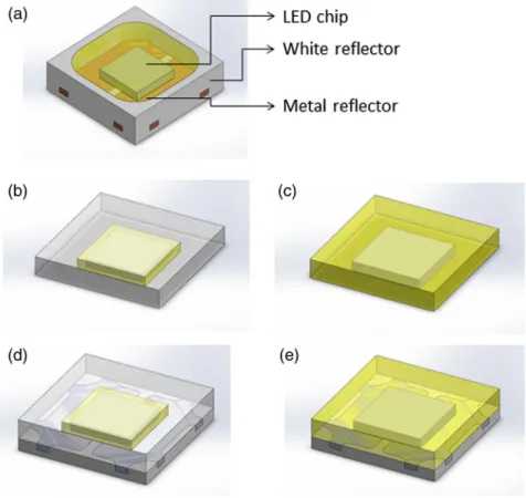
Fig. 1 Schematic diagram of the surface-mounted device (SMD) and chip-scale package (CSP) models: (a) SMD 3030, (b) bb-CSP with conformal phosphor, (c) bb-CSP with uniform phosphor, (d) rb-CSP with conformal phosphor, and (e) rb-CSP with uniform phosphor.
higher LEE, but also demonstrated the advantages of convenience in assembly similar to the SMD type.
To understand the light field distribution within various types of packaging, a simulation platform was established to evaluate the proposed CSP structure. Lighttools (Synopsys Optical Solutions) was used with the Monte Carlo method and Mie scattering33 to compare four models: three CSP structures and a conventional SMD package. Figure1shows a schematic diagram of the four models investigated in this study: (a) SMD 3030 package; (b) bb-CSP with a conformal phosphor structure; (c) bb-CSP with a uniform phosphor structure; (d) rb-CSP with a conformal phosphor structure; and (e) rb-CSP with uniform phosphor models. Near-field measurements of the light source of the chip were conducted for the simulation, in which the diameter of the phosphor particles was set at10.6 μm. Table 1 lists some of the related parameters. To consider the module efficiency according to the optical properties of the assembly surface, the assembly-dependent effect was defined by how heavily the efficiency depended on the assembly surface. This was considered because there is no reflector in the CSP structure; consequently, some light would be incident to the assembly surface, which is similar to a PCB. In the simulated model, the surface detector at the bottom of the CSP structure was employed to quantify the assembly-dependent effect, which shows the intensity on the assembly system. A far-field detector was also used to determine the LEE. Next, the cuboid size of the CSP structure with the conformal and uniform phosphor structures was adjusted to find the trend for a higher LEE and low assemble-dependent effect. Subsequently, the luminous efficacy of the CSP struc-tures and conventional SMD-type LED at various CCTs were calculated to be ∼10;000 K in BLU and <6500 K in lighting applications.
3 Results and Discussion
In general applications, LEDs are typically mounted on a PCB; thus, there is no influence regard-ing the type of SMD used because all of the photons originate from the top surface of the LED. CSP structures have no sidewall reflector to reflect the light; therefore, the assembly-dependent effect is defined as the change in an optical property at different distances. To evaluate the assembly-dependent effect, Fig.2 shows the energy distribution at the bottom surface of the CSP. The figure shows the energy distributions at the bottom of the bb-CSP and rb-CSP struc-tures. According to the calculations, the bb-CSP structure exhibited a high level of energy under the package because the rb-CSP has a lower assembly dependence compared with the bb-CSP structure. Generally, an assembly typically utilizes a PCB, but a PCB with a white painted sur-face is not as reflective as a white reflector in a CSP. Consequently, the backscattering light generated by a CSP structure is incident on the assembly surface, which can cause a considerable amount of optical energy loss in practical applications. However, the rb-CSP structure features a reflective surface that prevents light from becoming incident on the assembly surface and is effective in mitigating assembly dependence. Therefore, rb-CSP structures were employed as the main research object in this study. Furthermore, Fig.2also indicates that some optical energy would be incident on the assembly surface near the boundary of the CSP, and this is affected by the size of the cuboids and phosphor structures. For this shape, the cuboid size is critical because it can influence the performance of a device. Therefore, the LEE of the models was calculated with cuboids of various sizes.
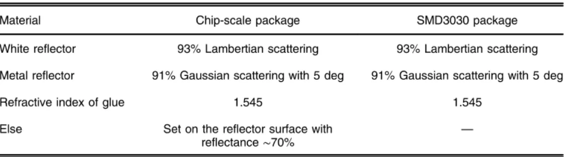
Table 1 Simulation model parameters.
Material Chip-scale package SMD3030 package White reflector 93% Lambertian scattering 93% Lambertian scattering Metal reflector 91% Gaussian scattering with 5 deg 91% Gaussian scattering with 5 deg Refractive index of glue 1.545 1.545
Else Set on the reflector surface with reflectance∼70%
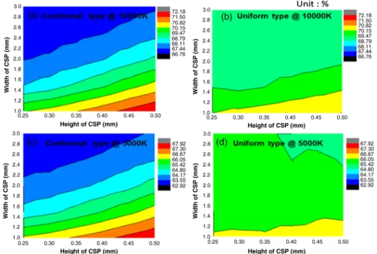
Figures3(a)–3(d)show the simulation result of the conformal rb-CSP with the CCT set at 10,000 K, a uniform rb-CSP with the CCT set at 10,000 K, a conformal rb-CSP with the CCT set at 5000 K, and a uniform rb-CSP with the CCT set at 5000 K, respectively. Conformal and uniform structures with various CSP heights and widths were set in the model to determine the efficiency trend. The simulation results showed that the efficiency of the conformal structure was more sensitive to the cuboid size than the uniform structure was because more backscatter-ing light was reflected toward the bottom surface and some of the energy was absorbed into the package. Increasing the CSP height and reducing the width increased the efficiency at both 5000 and 10,000 K. For the uniform structure, the efficiency is nearly independent of the CSP height and width. This can be attributed to the uniform distribution of the phosphor in the LED packaging.
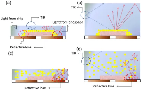
Figure4(a)–4(d)depict the light propagation in the following packages: a flat cuboid rb-CSP with a conformal phosphor structure; a higher cuboid rb-CSP with a conformal phosphor struc-ture, flat cuboid rb-CSP with uniform phosphor structure; and a higher cuboid rb-CSP with
Fig. 2 Intensity distributions on the assembly surfaces.
Fig. 3 Light extraction efficiency at various cuboid sizes: (a) CSP model with conformal phosphor in backlight unit (BLU) applications (10,000 K), (b) CSP model with uniform phosphor in BLU appli-cations (10,000 K), (c) CSP model with conformal phosphor in lighting appliappli-cations (5000 K), and (d) CSP model with uniform phosphor in lighting applications (5000 K).
uniform phosphor structure. The figure indicates that the rb-CSP with a higher cuboid height had less light incident on the bottom surface because of the increased height–width ratio. The same effect is evident in Figs.4(c)and4(d). In the CSP model, the optical energy was absorbed when the photons struck the bottom surface, which was the primary cause of energy loss. Two con-ditions must exist for light propagation to occur. First, part of the light emitted from the center of the rb-CSP is reflected because of the TIR. If TIR occurs at the top surface of the rb-CSP, then the reflected light is incident on the bottom surface of the rb-CSP. Under this condition, the light is partially absorbed. By contrast, when TIR occurs at another surface, the light is not directly emitted to the bottom surface of rb-CSP.
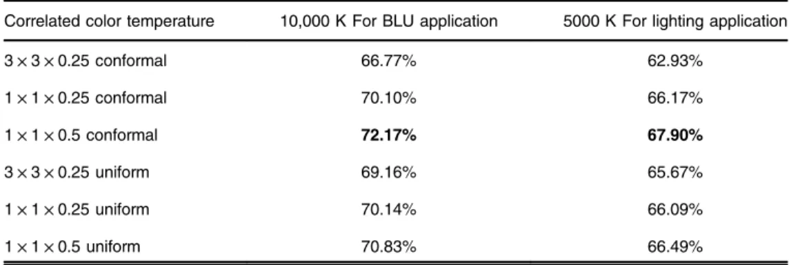
To quantify the assembly-dependence effect, Table2shows the LEE of CSP structures of various sizes and with different phosphor structures in BLU and lighting applications. A CSP with dimensions of3 × 3 × 0.25 mm3 and the rb-CSP with the conformal phosphor structure exhibited an LEE of ∼66.77% at 10,000 K and 62.93% at 5000 K. The higher LEE of the CSP structure with the higher CCT can be attributed to more light being converted from the phosphor through a downconversion process in the low-CCT structure, and the energy is consumed when the shorter wavelength is converted to a longer wavelength.34
In Table 2, the result shows that the reduced-area CSP (1 × 1 × 0.25 mm3) with the con-formal and uniform phosphor structures successfully improved the LEE by 4 and 1%, respec-tively. Moreover, the efficiency of the conformal and uniform rb-CSP structures can be increased by 2 and 0.7%, respectively, as the height is increased from 0.25 to 0.5 mm. Therefore, the LEE of the conformal structure was superior to that of the uniform structure when the height of the CSP was increased by a sufficient amount, and reducing the area of the CSP structure is a useful method for improving the LEE. By contrast, the total quantity differed between the conformal and uniform structures because the phosphor light was pumped by a blue-ray laser. The con-formal structure exhibited the densest phosphor distribution near the chip. Thus, the concon-formal structure can utilize the smaller quantity of phosphor more effectively than the uniform structure to achieve the same CCT.
To determine the optimal LEE, Fig.5shows the LEE of the CSP structures of various heights. The optimal height of the CSP model is∼1 mm, which improved the LEE to 4%. Moreover, the LEE was almost saturated when the height was 1 mm. Figures 5(a)–5(c)show the ray trace analysis of the rb-CSP structures of various heights: 0.8, 0.5, and 0.3 mm. Compared with these results, more light is incident on the bottom surface in the 0.3-mm-high rb-CSP structure compared with the taller rb-CSP structures. In summary, the size of the CSP structure is crucial in optimizing the design.
Fig. 4 Schematic propagation depicting the path of light in the CSP models: (a) flat cuboid rb-CSP with conformal phosphor, (b) tall cuboid rb-CSP with conformal phosphor, (c) flat cuboid rb-CSP with uniform phosphor, and (d) tall cuboid rb-CSP with uniform phosphor.
Figure6shows the luminous efficacy of SMD-type and CSP structures at various CCTs. The rb-CSP structures have a higher luminous efficiency compared with the SMD type. Compared with the SMD type, the CSP structures enhanced the luminous efficiency by 8.81% in lighting applications and 9.43% in BLU applications. In the SMD type, the light was reflected several times within the package, and some of the energy was absorbed by the white reflector and bottom surface because of the bowl structure; therefore, the SMD type has a lower efficiency because of the loss of trapped photons in the package. Conversely, although the efficiency of the CSP
Table 2 Light extraction efficiency in backlight unit (BLU) and lighting applications.
Correlated color temperature 10,000 K For BLU application 5000 K For lighting application
3 × 3 × 0.25 conformal 66.77% 62.93% 1 × 1 × 0.25 conformal 70.10% 66.17% 1 × 1 × 0.5 conformal 72.17% 67.90% 3 × 3 × 0.25 uniform 69.16% 65.67% 1 × 1 × 0.25 uniform 70.14% 66.09% 1 × 1 × 0.5 uniform 70.83% 66.49%
Note: The bold values indicate the highest efficiency design of these structures of CSP. We optimized the design of CSP from the result of various sizes design.
Fig. 5 CSP height and ray trace analysis results: (a) 0.8 mm, (b) 0.5 mm, and (c) 0.3 mm.
Fig. 6 Result of luminous efficacy of the CSP and SMD-type structures at various correlated color temperatures.
structures exhibited a slight loss because of the backscattering light, the optimal CSP design exhibited a higher LEE compared with the SMD type.
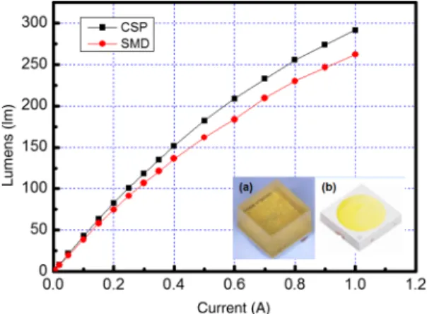
To improve the accuracy of the simulation model, the CSP and SMD-type structures were prepared. Figure7shows the experimental result of CSP and SMD type at 5700 K. The dimen-sions of the CSP and SMD-type structures are1.3 × 1.3 × 1.0 and 3.0 × 3.0 × 0.6 mm3, respec-tively. The result shows that at 350 mA, using the CSP structure enhanced the LEE by∼10% compared with using the SMD-type structure. Thus, this measurement verifies the simulation and experimental results for both structures.
4 Conclusion
In this study, the designs of CSP models with conformal and uniform structures were demon-strated at various CCTs. The results show that the CSP structure achieved a higher LEE and lower assembly-dependence effect compared with the conventional SMD type. This occurred because the bowl structure of the SMD type caused some energy loss. Accordingly, the effi-ciency of the reflective-bottom CSP model with a small area and greater height was 8.81 and 9.43% higher than that of the conventional SMD-type structure at CCTs of 5000 and 10,000 K, respectively. Thus, the proposed CSP model offers high potential as a lighting source in both lighting and BLU applications.
Acknowledgments
This work was funded by the National Science Council, Taiwan (Grant Numbers NSC102-3113-P-009-007-CC2 and NSC102-2221-E-009-131-MY3).
References
1. E. F. Schubert and J. K. Kim,“Solid-state light sources getting smart,”Science308, 1274– 1278 (2005).
2. K. J. Chen et al.,“An investigation of the optical analysis in white light-emitting diodes with conformal and remote phosphor structure,”J. Disp. Technol.9, 915–920 (2013). 3. S. Pimputkar et al., “Prospects for LED lighting,”Nat. Photonics3, 179–181 (2009). 4. K. J. Chen et al.,“High thermal stability of correlated color temperature using current
com-pensation in hybrid warm white high-voltage LEDs,”Opt. Express21, A201–A207 (2013). 5. H. C. Kuo et al.,“Patterned structure of REMOTE PHOSPHOR for phosphor-converted
white LEDs,”Opt. Express19, A930–A936 (2011).
6. H. C. Chen et al.,“A novel randomly textured phosphor structure for highly efficient white light-emitting diodes,”Nanoscale Res. Lett. 7, 1–5 (2012).
Fig. 7 Luminous flux of the CSP and SMD-type structures at 5700 K: (a) CSP sample and (b) SMD sample.
7. D. W. Lin et al., “Enhanced light output power and growth mechanism of GaN-based light-emitting diodes grown on cone-shapedSiO2 patterned template,”J. Disp. Technol.
9, 285–291 (2013).
8. C. H. Wang et al.,“Hole injection and efficiency droop improvement in InGaN/GaN light-emitting diodes by band-engineered electron blocking layer,”Appl. Phys. Lett.97, 261103 (2010).
9. R. M. Farrell et al., “Materials and growth issues for high-performance nonpolar and semipolar light-emitting devices,”Semicond. Sci. Technol. 27, 024001 (2012).
10. R. A. Arif, Y.-K. Ee, and N. Tansu,“Polarization engineering via staggered InGaN quantum wells for radiative efficiency enhancement of light emitting diodes,”Appl. Phys. Lett.91, 091110 (2007).
11. H. Zhao et al.,“Approaches for high internal quantum efficiency green InGaN light-emitting diodes with large overlap quantum wells,”Opt. Express 19(S4), A991–A1007 (2011). 12. D. S. Wuu et al.,“Defect reduction and efficiency improvement of near-ultraviolet emitters
via laterally overgrown GaN on a GaN/patterned sapphire template,”Appl. Phys. Lett.89, 161105 (2006).
13. Y. J. Lee et al., “Enhancing the output power of GaN-based LEDs grown on wet-etched patterned sapphire substrates,”IEEE Photon. Technol. Lett.18, 1152–1154 (2006). 14. S. Choi et al.,“Efficiency droop due to electron spill-over and limited hole injection in
III-nitrid visible light-emitting diodes employing lattice-matched InAlN electron blocking layers,”Appl. Phys. Lett. 101(16), 161110 (2012).
15. G. Liu et al.,“Efficiency-droop suppression by using large-bandgap AlGaInN thin barrier layers in InGaN quantum-well light-emitting diodes,” IEEE Photonics J. 5, 2201011 (2013).
16. H. Zhao et al.,“Analysis of internal quantum efficiency and current injection efficiency in III-nitride light-emitting diodes,”J. Disp. Technol.9, 212–225 (2013).
17. C. H. Chiu et al., “High efficiency GaN-based light-emitting diodes with embedded air voids/SiO2 nanomasks,”Nanotechnology23, 045303 (2012).
18. C. H. Chiu et al.,“Highly efficient and bright LEDs overgrown on GaN nanopillar sub-strates,”IEEE J. Sel. Topics Quantum Electron.17, 971–978 (2011).
19. C. F. Lai et al.,“CCT- and CRI-tuning of white light-emitting diodes using three-dimen-sional non-close-packed colloidal photonic crystals with photonic stopbands,”Opt. Express
21, A687–A694 (2013).
20. H. K. Park, J. H. Oh, and Y. R. Do,“Toward scatter-free phosphors in white phosphor-converted light-emitting diodes,”Opt. Express20, 10218–10228 (2012).
21. Y. K. Ee et al.,“Metalorganic vapor phase epitaxy of III-nitride light-emitting diodes on nano-patterned AGOG sapphire substrate by abbreviated growth mode,”IEEE J. Sel. Topics Quantum Electron.15(4), 1066–1072 (2009).
22. Y. Li et al., “Defect-reduced green GaInN/GaN light-emitting diode on nanopatterned sapphire,”Appl. Phys. Lett.98(15), 151102 (2012).
23. K. J. Chen et al.,“Resonant-enhanced full-color emission of quantum-dot-based display technology using a pulsed spray method,”Adv. Funct. Mater. 22, 5138–5143 (2012). 24. Y. H. Won et al.,“Effect of phosphor geometry on the luminous efficiency of high-power
white light-emitting diodes with excellent color rendering property,”Opt. Lett. 34, 1–3 (2009).
25. T. Fukui et al.,“Superior illuminant characteristics of color rendering and luminous efficacy in multilayered phosphor conversion white light sources excited by near-ultraviolet light-emitting diodes,”Jpn. J. Appl. Phys.48, 112101 (2009).
26. J. P. You, N. T. Tran, and F. G. Shi,“Light extraction enhanced white light-emitting diodes with multi-layered phosphor configuration,”Opt. Express18, 5055–5060 (2010). 27. C.-W. Sher et al.,“Enhancement of luminous efficiency by hybrid structure for warm white
light-emitting diodes,”J. Solid State Lighting1, 9 (2014)
28. M. R. Krames et al.,“Status and future of high-power light-emitting diodes for solid-state lighting,”J. Disp. Technol. 3, 160–175 (2007).
29. H. T. Huang, C. C. Tsai, and Y. P. Huang,“Conformal phosphor coating using pulsed spray to reduce color deviation of white LEDs,”Opt. Express18, A201–A206 (2010).
30. G. Bogner, A. Debray, and K. Hoehn,“High-performance epoxy casting resins for SMD-LED packaging,”Proc. SPIE 3938, 249–261 (2000).
31. K. J. Chen et al.,“Effect of the thermal characteristics of phosphor for the conformal and remote structures in white light-emitting diodes,”IEEE Photonics J. 5, 8200508 (2013). 32. N. T. Tran and F. G. Shi,“Studies of phosphor concentration and thickness for phosphor-based white light-emitting-diodes,”IEEE Lightwave Technol. J. 26, 3556–3559 (2008). 33. C.-C. Sun et al.,“Precise optical modeling for silicate-based white LEDs,”Opt. Express
16, 20060–20066 (2008).
34. K.-J. Chen et al.,“Efficiency and droop improvement in hybrid warm white LED using InGaN and AlGaInP high-voltage LEDs,”J. Disp. Technol. 9, 280–284 (2013).
Che-Hsuan Huangis a PhD student in the Institute of EO engineering, National Chiao Tung University, Hsinchu. Now his research interests include LED package structure design, optic and stress analysis, and application design for novel LED source.
Min-Ta Tsai is a PhD student at the Department of Electrophysics, National Chiao Tung University, Hsinchu. From 2000 to 2006, he worked with TFT Product and Array/Cell Process and Design, AUO, Hsinchu, Taiwan, and from 2006 to 2009, he worked with LED Package Structure Design, AUO Group, Hsinchu, Taiwan. His research interests include LED package structure design, heat and mass transfer, and package process design and LED lighting design.
Wei-I Leereceived the BS degree from National Chiao Tung University, Hsinchu, Taiwan, in 1981, the MS degree from the University of Wisconsin at Madison in 1985, and the PhD degree in electrical engineering from Rensselaer Polytechnic Institute, Troy, NY, in 1988. He is pro-fessor in the Department of Electro-Physics, National Chiao Tung University, Hsinchu. He served as a research engineer at the Varian Research Center, Palo Alto, CA, from 1988 to 1991. He then joined National Chiao Tung University in 1991. His current research interests include semiconductor material growth and device fabrication.