Microstructure and Nonlinear Properties of Microwave-Sintered
ZnO–V
2O
5Varistors: II, Effect of Mn
3O
4Doping
Cheng-Tzu Kuo, Chang-Shun Chen,
†and I-Nan Lin
‡ Institute of Materials Science and Engineering, National Chiao-Tung University, Hsinchu, Taiwan 300, Republic of ChinaThe microstructure and nonlinear current–voltage charac-teristics of Mn3O4-doped ZnO–V2O5ceramics,
microwave-sintered at 800°–1200°C for 10 min, have been investigated. A high density (96% of the theoretical density) has been achieved. The incorporation of Mn3O4 additives does not
significantly alter the densification behavior of the ZnO– V2O5materials, but rather pronouncedly increases the
non-linear coefficient (␣ = 23.5) and markedly suppresses their leakage current density (JL = 2.4 × 10⁻⁶ A/cm2). On the
other hand, the intrinsic properties of the materials, includ-ing the Schottky barrier height (⌽b) and the donor density
(Nd), are only moderately modified; that is,⌽b= 1.16 eV
and Nd= 5.4 × 10¹⁷/cm3. X-ray diffractometry analyses and
energy-dispersive X-ray microanalyses (via scanning elec-tron microscopy) indicate that the V2O5 species facilitate
the densification and the development of microstructure via the formation of a liquid phase (Zn3(VO4)2) along the grain
boundaries, whereas the Mn3O4species markedly enhance
the nonohmic behavior of the ZnO–V2O5 materials by
forming the surface states along the grain boundaries. I. Introduction
Z
INC OXIDE (ZnO) materials are important n-typesemicon-ductors; they are used as varistor materials, because of their highly nonohmic behavior in current–voltage (I–V ) character-istics with an excellent capability of withstanding surges.1–5
Therefore, ZnO-based varistors are extensively used as tran-sient surge suppressors against dangerous abnormal high volt-age surges, to protect electronic circuits.6–11It is believed that
the nonlinear I–V characteristics of these materials result from the grain-boundary layer, which is essentially formed by a segregation of large ionic additives, such as Bi2O3, Pr6O11, and
BaO, at the grain boundary.12–16 These ‘‘varistor-forming’’
ingredients affect the electrical properties and the densification behavior and microstructure evolution of ZnO ceramics. Fur-thermore, MnO2 additives are generally included to improve
the nonohmic properties of ceramics by increasing the surface-state density.17,18
Recently, it was reported that V2O5 is another
varistor-forming ingredient for ZnO ceramics;19its use results in
varis-tor properties that are similar to those of ZnO–Bi2O3ceramics.
The advantage of the ZnO–V2O5system is that the materials
can be sintered at relatively low temperature (i.e.,∼900°C) in a conventional electrical furnace. This property is important for
applications of multilayer chip components, because the mate-rial can be cofired with a silver inner electrode, which has melting point of∼961°C.
It is generally known that the microwave sintering process can densify ceramic materials at a very rapid rate;20–23thus,
this process has been adopted in this work to prepare the ZnO– V2O5–Mn3O4ceramics. We have conducted an extensive
ex-amination on the effect of sintering temperature and soaking time on the densification behavior of these materials. The cor-relation between the microstructure characteristics of the materials and their I–V and capacitance–voltage (C–V ) be-haviors is discussed, with an emphasis on the role of Mn3O4
incorporation.
II. Experimental Procedures
High-purity ZnO varistor powders (>99.9%) were prepared. The mixtures were composed of ZnO–V2O5materials that
con-tained 0.5 mol% V2O5and x mol% Mn3O4(where x⳱ 0–1.0).
The mixtures were ball-milled in a plastic jar, using zirconia balls and deionized water, for 8 h. After the mixtures were filtered and dried, they were calcined at 700°C in air for 2 h, followed by pulverization in a ball mill for 8 h to a size of∼1.0
m; the mixtures were than uniaxially pressed at 750 kgf/cm2
into a disk 8 mm in diameter and 2 mm thick. The green pellets, which were ∼60% of the theoretical density (TD ⳱ 5.675 g/cm3) were microwave-sintered at 800°–1200°C for 5–60 min
in an applicator that was made of a WR284 waveguide (Gerling Co., Modesto, CA), using a 2.45 GHz microwave generated from a commercial source (Model GL107 magnetron, Gerling). The temperature profile was measured by using a Pt–13% Rh thermocouple that was placed near the sample surface. The heating rate was controlled at 60°C/min, and the cooling rate was controlled at 145°C/min for sintering temperatures >500°C. The details of the apparatus used for the microwave sintering process are described elsewhere.24For comparison,
the samples were also prepared via a conventional sintering process; that is, sintering at 900°–1200°C for 60 min in an electrical furnace. The heating rate and the cooling rate for this latter process each were 5°C/min.
The crystal structure and microstructure of the sintered samples were examined using X-ray diffractometry (XRD) (Model XD-5, Shimadzu Co., Kyoto, Japan) and scanning elec-tron microscopy (SEM) (Model JSM-840A, JEOL, Tokyo, Ja-pan), respectively. The density of sintered specimens was mea-sured by using the Archimedes method. The average grain size (G) was calculated as described by Mendelson,25with a
mul-tiple factor of 1.56. The I–V properties of these samples were recorded by using an electrometer (Model 237 I-V, Keithley Instruments, Cleveland, OH) in dc source after the indium– gallium (40:60) alloy was rubbed onto the sample surface to serve as electrodes. The onset electric field (E0) was measured
at a current density of 1.0 mA/cm2, the nonlinear coefficient
(␣) was estimated for current-density ranges of 1.0–10 mA/ cm2, and the leakage current density (J
L) was defined as the
current density at an applied field of 10 V/mm. The C–V mea-surements were made at room temperature using a capacitance
L. M. Levinson—contributing editor
Manuscript No. 191065. Received April 21, 1997; approved February 5, 1998. Supported by the National Science Council of the Republic of China (ROC) through Grant No. NSC 86-2221-E-009-041.
†Now with Department of Mechanical Engineering, Hwa-Hsia College of
Tech-nology and Commerce, Taipei, Taiwan 235, ROC.
‡Now with Materials Science Center, National Tsing-Hua University, Hsinchu,
Taiwan 300, ROC.
Journal
meter (Model HP4274A, Hewlett–Packard, Tokyo, Japan). The electrical characteristics, which include the Schottky barrier height⌽band the donor density Nd, were determined from the
C–V data, using the model proposed by Mukae et al.26
III. Results (1) Sintering Behavior
As reported previously, the incorporation of V2O5additives
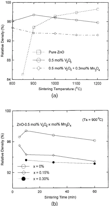
markedly enhances the densification rate of the ZnO materials. Figure 1(a) shows that only 800°C (for 10 min) is required in the microwave sintering process for these materials to attain a density as high as 96.1% of the theoretical density (TD) for ZnO–0.5-mol%-V2O5materials, whereas at least 900°C (for 10
min) is required to attain high density for pure ZnO materials. Increasing the sintering temperature, from 800°C to 1200°C (for 10 min), and the soaking time, from 5 min to 60 min (at 900°C), only moderately alters the densification behavior of the ZnO–V2O5 materials, as shown in Figs. 1(a) and (b),
re-spectively. Moreover, the incorporation of Mn3O4only slightly
reduces the sintered density without significantly modifying the temperature and time dependence of the sample density.
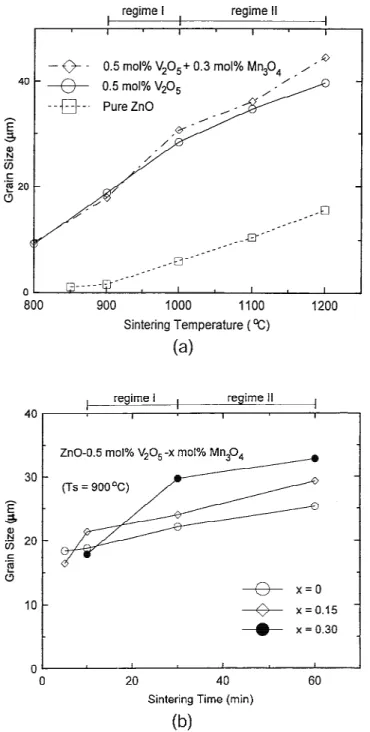
The grain-growth rate of the ZnO materials is also signifi-cantly increased because of the V2O5addition. SEM
examina-tion shows that, when microwave-sintered at 900°C for 10 min, the grains of pure ZnO materials hardly grow; however, the ZnO–0.5-mol%-V2O5materials have already developed a large
grain size (∼18.8m). The incorporation of an additional 0.3 mol% of Mn3O4does not significantly affect the grain-growth
rate of these materials. Figs. 2(a)–(d) reveal that a higher sin-tering temperature monotonously increases the grain size of the ZnO–V2O5–Mn3O4samples, and Figs. 2(a), (e), and (f) further
indicate that a longer soaking time also results in a larger grain size for these samples. The effect of the microwave sintering temperature and the soaking time on the grain-growth behavior of these material is more clearly illustrated in Figs. 3(a) and (b), respectively. The grain size increases markedly, from 18.8m to 30 m, when the sintering temperature increases from 900°C to 1000°C or the soaking time extends from 10 min to 30 min (regime I in Fig. 3). The change in grain size is less pronounced beyond this range (regime II in Fig. 3). Their sig-nificance on the electrical properties of the ZnO materials will be discussed shortly.
On the other hand, the proportion of Mn3O4additives that
are incorporated into the ZnO–0.5 mol% V2O5 does not
sig-nificantly modify the densification and grain-growth behaviors of these materials, as shown in Figs. 4(a) and (b), respectively. The density of the ZnO–V2O5–Mn3O4 materials varies in the
range of 92.5%–94.5% of TD, whereas their grain size varies in the range of 15.5–21 m for the samples that contain ∼1.0 mol% Mn3O4 and have been microwave-sintered (ms) at
900°C for 10 min. For comparison, the characteristics of the ZnO–V2O5–Mn3O4 materials densified via the conventional
furnace sintering (fs) process are also shown in Figs. 4(a) and (b); this comparison indicates that a pronouncedly longer sin-tering time (i.e., 60 min at 900°C) is required for the fs samples to achieve the same density as the ms samples, at 900°C for 10 min. Moreover, the resultant grain size of the fs samples (3–5
m) is markedly smaller than that of the ms samples, which
implies that grain-boundary mobility is low in the fs process but is markedly enhanced in the ms process.
The fact that the V2O5additives can enhance the
densifica-tion and grain-growth behaviors of the ZnO–V2O5 materials
has been considered by the formation of a ZnO–V2O5
com-pound, i.e., Zn3(VO4)2, which acts as a liquid-phase sintering
aid at high temperature.15,16Such a phenomenon also has been
examined in ZnO–V2O5–Mn3O4 materials via the XRD and
EDAX microanalytic techniques. Typical phase constituents of these materials are represented by the XRD patterns of the microwave-sintered ZnO–V2O5 (0.5 mol%)–Mn3O4 (0.3
mol%) materials in Fig. 5(a); these XRD patterns reveal the presence of a Zn3(VO4)2 secondary phase, in addition to the
hexagonal ZnO. No secondary phase related to Mn3O4 is
detected.
The EDAX microanalyses shown in Fig. 5(b) for 900°C (for 30 min) microwave-sintered ZnO–0.5-mol%-V2O5
–0.3-mol%-Mn3O4samples indicate that, in addition to the zinc species, the
vanadium and manganese species both can be observed at the grain-boundary regions (pattern ‘‘1’’ in Fig. 5(b)), whereas only the manganese species are detectable, in addition to the main constituents (the zinc species), in the grain interior (pat-tern ‘‘2’’ in Fig. 5(b)). A similar phenomenon has been ob-served for the samples microwave-sintered at 1200°C (for 10 min), as shown in the EDAX microanalyses in Fig. 5(c), which reveals, again, that the vanadium and manganese species both are detected at the junction of the grains (pattern ‘‘1’’ in Fig. 5(c)) and only the manganese species coexist with the zinc species in the grain interior (pattern ‘‘2’’ in Fig. 5(c)). There is a clear implication that the V2O5additives only reside at the
grain-boundary region and will eutectically react with the ZnO
Fig. 1. Variation of the density of ZnO–V2O5–Mn3O4materials with
(a) the microwave sintering temperature (with a soaking time of 10 min) and (b) the soaking time (microwave-sintered at 900°C).
materials in this region. This phenomenon is in agreement with the proposed model: that is, the V2O5additives have enhanced
the densification and grain-growth processes via the formation of a liquid phase at the sintering temperature. The significance of the phenomenon that the manganese species reside both at the grain boundaries and in the grain interior will be discussed shortly.
(2) Electrical Properties
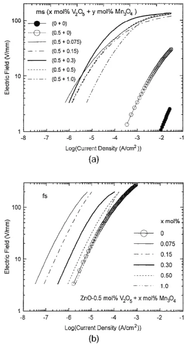
The effect of V2O5 and Mn3O4 addition on the electrical
properties of the ZnO materials has been characterized. As shown in Fig. 6(a), for the materials that have been
microwave-sintered at 900°C for 10 min, the V2O5 additives markedly
suppress the leakage current density (JL) of the pure ZnO
ma-terials (cf. solid and open circles in Fig. 6(a)). The incorpora-tion of the Mn3O4 species further reduces the value of JLby
more than 3 orders of magnitude, which results in prominent nonohmic characteristics. For comparison, the effect of these additives on the electrical behavior of the conventionally sin-tered ZnO–V2O5–Mn3O4 materials (900°C for 60 min) is
shown in Fig. 6(b). Generally, the furnace-sintered samples possess inferior ␣ values, in comparison to the microwave-sintered materials, although they have smaller JLvalues. These
behaviors are closely related to the smaller grain size of the Fig. 2. SEM micrographs of the ZnO–0.5-mol%-V2O5–0.3-mol%-Mn3O4materials microwave-sintered at (a) 900°, (b) 1000°, (c) 1100°, and (d)
1200°C for 10 min, showing the effect of sintering temperature; Figs. 2(e) and (f ) are SEM micrographs of ZnO–V2O5–Mn3O4 materials
microwave-sintered at 900°C for 30 and 60 min, respectively, showing the effect of soaking time.
furnace-sintered samples (cf. Fig. 4); one can infer from this comparison that the donor additives can be fully incorporated into the grain interior of the samples only when pronounced grain-boundary migration has occurred. The advantage of the microwave sintering process over the conventional furnace sin-tering process in the preparation of ZnO varistor materials is, again, ascribed to the implied enhancement of the sintering process. Figure 6(b) reveals that the incorporation of Mn3O4
additives also significantly reduces the JL values of the
fur-nace-sintered samples.
To examine the effect of Mn3O4 doping on the electrical
properties of the ZnO–V2O5materials more clearly, the values
of␣ and JLfor the samples are derived from the E–J curves
that are shown in Fig. 6(a), whereas the values of⌽band Ndfor
the samples are derived from their capacitance–voltage (C−2– V ) characteristics (not shown). Figure 7(a) shows that JLvaries
only moderately with the proportion of Mn3O4additives (i.e.,
JL ⳱ 0.34 × 10⁻⁵–2.0 × 10⁻⁵ A/cm2); however, ␣ shows a
maximum value for the samples that are doped with 0.3 mol% of Mn3O4(i.e.,␣ ⳱ 17.8). By contrast, Fig. 7(b) shows that ⌽b
and Nd both possess a minimum value for the
0.3-mol%-Mn3O4-doped composition: that is,⌽b⳱ 0.93 eV and Nd⳱
0.8 × 1018cm−3.
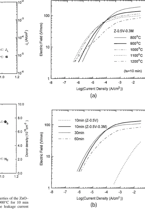
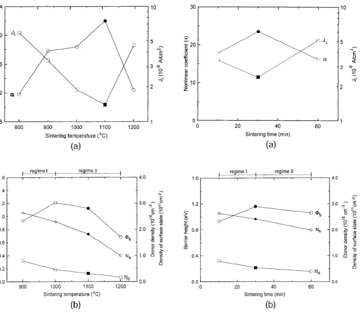
The effect of the sintering temperature and the soaking time on the electrical properties of the ZnO–0.5-mol%-V2O5
–0.3-mol%-Mn3O4materials has been examined further. The
result-ant E–J behaviors are shown in Figs. 8(a) and (b), respectively; these figures indicate that most of the samples possess good nonohmic properties, except for those where the microwave sintering temperature is too high (i.e., 1200°C for 10 min; see Fig. 8(a)) or the soaking time is too long (i.e., 60 min at 900°C; see Fig. 8(b)). The important electronic parameters of these materials are derived from the E–J curves and the correspond-ing C–V curves (not shown). The results are plotted in Figs. 9 and 10; these figures indicate that the ␣ and JL values are
optimized for the samples sintered at 1100°C (10 min) and 900°C (30 min) (closed circles in Figs. 9 and 10). These values are as follows: ␣ ⳱ 22–23.5, JL ⳱ 1.4 × 10⁻⁶–2.4 × 10⁻⁶
A/cm2;⌽
b⳱ 0.93–1.21 eV, and Nd⳱ 0.31 × 10¹⁸–0.54 × 10¹⁸
Fig. 3. Variation of the grain size of the ZnO–V2O5–Mn3O4
mate-rials with (a) the sintering temperature (for a soaking time of 10 min) and (b) the soaking time (sintered at 900°C).
Fig. 4. Variation of (a) sintered density and (b) grain size with the Mn3O4content in ZnO–V2O5–Mn3O4 materials densified by either
microwave sintering at 900°C for 10 min or conventional furnace sintering for 60 min.
cm−3. The nonohmic properties of the insufficiently sintered or
overfired samples (open circles in Figs. 9 and 10) are inferior to those of the properly sintered samples. In other words, the processing parameters significantly affect the nonohmic prop-erties of the ZnO–V2O5–Mn3O4 materials. Because all the
samples are of high density, the modification on the nonohmic behavior of the materials is, most likely, a result of the change in the defect chemistry along their grain boundaries, which will be discussed shortly.
IV. Discussion
It is generally believed that, in the ZnO materials, the donors are the zinc species that occupy the interstitial sites of the lattice (i.e., Zni). The proportion of these species can be altered
most easily via outward diffusion of these species via the post-annealing process. Moreover, the effective donor density (Nd)
can also be reduced, because of the presence of the electron
Fig. 6. Effect of Mn3O4 additives on the
electric-field–current-density (E–J) characteristics of the ZnO–0.5-mol%-V2O5 materials
obtained via (a) microwave sintering at 900°C for 10 min and (b) conventional furnace sintering at 900°C for 60 min.
Fig. 5. (a) XRD patterns (CuK␣) of ZnO–0.5-mol%-V2O5
–0.3-mol%-Mn3O4materials microwave-sintered at 800°–1200°C (for 10
min) or 900°C (for 60 min); Figs. 5(b) and (c) are EDAX (in SEM) patterns of the same materials microwave-sintered at 900°C for 30 min and 1200°C for 10 min, respectively.
traps, which are, most probably, manganese ions that have partially dissolved into the matrix. By contrast, the manganese species have a tendency to remain at the grain boundaries (i.e., Mngb), which forms the surface states. Therefore, a
re-duction in surface-state density (Ns) can occur, because of the
partial dissolution of the manganese ions into the grains or the loss of the Mngb species that accompanies the volatile
vana-dium species.
Because the proportion of donor (Zni) and acceptor (Mn)
species that are incorporated in these samples is the same, the only possible reaction that can occur during sintering is a re-distribution of these species. Pronounced grain growth that occurs during sintering (cf. Table I) will induce rapid grain-boundary migration. Thus, a significant proportion of manga-nese ions that had originally resided at the grain boundaries is left behind and dissolved into the grains, which results in a decrease in the value of Nd.
Moreover, a loss of the manganese species through vapor-ization will occur, in addition to an inward diffusion of the manganese species into the grains, for the samples that have been sintered at high temperature (or for long soaking times).
Such a phenomenon leads to a significant reduction in the value of Nsfor samples sintered at 1200°C (for 10 min) and explains
the significant degradation of the nonlinear properties of these materials very well.
The above-mentioned discussions clearly indicate that the processing parameters that have been used to sinter the ZnO– V2O5–Mn3O4materials markedly modify the defect chemistry
along grain boundaries, which significantly alters the nonohmic properties of the materials. This phenomenon occurs mainly via redistribution of the additives.
V. Conclusion
The effect of V2O5and Mn3O4additives on the densification
behavior and the grain-growth characteristics of the ZnO ma-terials, and their associated nonohmic properties, were
system-Fig. 7. Effect of Mn3O4additives on various properties of the ZnO–
0.5-mol%-V2O5 materials microwave-sintered at 900°C for 10 min
((a) (䊊) the nonlinear coefficient (␣) and (䊐) the leakage current density (JL); (b) (䊊) the potential barrier height (⌽b) and (䊐) the
donor density (Nd)). Fig. 8. Effect of (a) the microwave sintering temperature (800°–
1200°C for 10 min) and (b) the soaking time (10–60 min at 900°C) on the electrical-field–current-density (E–J ) characteristics of ZnO–0.5-mol%-V2O5–0.3-mol%-Mn3O4 materials (the dashed curve in Fig.
8(b) represents the E–J characteristics of ZnO–0.5-mol%-V2O5
mate-rials).
atically examined. The addition of V2O5markedly reduced the
microwave sintering temperature and soaking time necessary to densify the ZnO materials and induce grain growth. The incor-poration of the Mn3O4 species did not significantly modify
their sintering properties but did markedly alter their nonohmic behavior. The proper processing parameters, such as the mi-crowave sintering temperature (900°C) and soaking time (30 min), further improved the nonlinear coefficient␣ and the
leak-age current density JLthrough modification of the defect
chem-istry of the samples. References
1M. Matsuoka, ‘‘Nonohmic Properties of Zinc Oxide Ceramics,’’ Jpn. J.
Appl. Phys., 10 [6] 736–46 (1971).
2M. Inada, ‘‘Crystal Phases on Non-ohmic Zinc Oxide Ceramics,’’ Jpn. J.
Appl. Phys., 17 [1] 1–10 (1978).
Fig. 9. Effect of the microwave sintering temperature (800°–1200°C for 10 min) on various properties of ZnO–0.5-mol%-V2O5
–0.3-mol%-Mn3O4materials ((a) (䊊) the nonlinear coefficient (␣) and (䊐) the
leakage current density (JL); (b) (䊉) the potential barrier height (⌽b),
(䊏) the donor density (Nd), and (⽧) the surface-state density (Ns)).
Fig. 10. Effect of soaking time (10–60 min for 900°C) on various properties of the ZnO–0.5-mol%-V2O5–0.3-mol%-Mn3O4 materials
((a) (䊏) nonlinear coefficient (␣) and (䊉) leakage current density (JL);
(b) (䊉) potential barrier height (⌽b), (䊏) donor density (Nd), and (⽧)
surface-state density (Ns)).
Table I. Variation of Donor and Surface-State Density (Ndand Ns, Respectively) with Sintering Conditions
Sintering conditions Grain size (m) Nd (× 1018cm−3) (× 1011Nscm−2) ␣ ⌽ b(eV) Remark 900°C, 10 min 17.9 0.80 2.64 17.8 0.93 1000°C, 10 min 30.7 0.46† 2.29 18.4 1.21 Regime I in Fig. 3† 1100°C, 10 min 36.1 0.31 1.81 22.0 1.12 1200°C, 10 min 44.6 0.16 1.00‡ 12.4 0.68 Regime II in Fig. 3‡ 900°C, 10 min 17.9 0.80 2.64 17.8 0.93 900°C, 30 min 29.7 0.54† 2.42 23.5 1.16 Regime I in Fig. 3† 900°C, 60 min 32.8 0.40 1.99‡ 16.2 1.06 Regime II in Fig. 3‡ †Marked reduction in N
ddue to grain growth.‡Marked reduction in Nsdue to manganese loss.
3L. M. Levinson and H. R. Philipp, ‘‘Zinc Oxide Varistors—A Review,’’ Am.
Ceram. Soc. Bull., 65 [4] 639–46 (1986).
4T. K. Gupta, ‘‘Application of Zinc Oxide Varistors,’’ J. Am. Ceram. Soc., 73 [7] 1817–40 (1990).
5K. Eda, A. Iga, and M. Matsuoka, ‘‘Degradation Mechanism of Non-ohmic Zinc Oxide Ceramics,’’ J. Appl. Phys., 51 [5] 2678–84 (1980).
6J. Erickson and B. Reich, ‘‘The High Power Metal-Oxide Varistor as a Vehicle and Aircraft Transient Suppressor,’’ IEEE Trans. Aerosp. Electron.
Syst., AES-12, 104–108 (1976).
7L. M. Levinson and H. R. Philipp, ‘‘ZnO Varistors for Transient Protec-tion,’’ IEEE Trans. Parts, Hybrids, Packag., PHP-13, 338–43 (1977).
8E. C. Sakshaug, J. S. Kresge, and S. A. Miske, ‘‘A New Concept in Station Arrestor Designs,’’ IEEE Trans. Power Appar. Syst., PAS-96, 647–56 (1977).
9R. Einzinger, ‘‘Metal Oxide Varistors,’’ Annu. Rev. Mater. Sci., 17, 299–321 (1987).
10J. E. May, ‘‘Properties of 3 Volt Zinc Oxide Varistors’’; pp. 295–305 in Ceramic Transactions, Vol. 3, Advances in Varistor Technology. Edited by L. M. Levinson, American Ceramic Society, Westerville, OH, 1989.
11J. Ozawa, T. Yamazaki, S. Maruyama, S. Shirakawa, A. Mizukoshi, and K. Nakano, ‘‘Applications of Zinc Oxide Nonlinear Elements’’; ibid, pp. 256–65. 12P. Williams, O. L. Krivanek, G. Thomas, and M. Yodogawa, ‘‘Microstruc-ture–Property Relationships of Rare-Earth-Zinc-Oxide Varistors,’’ J. Appl.
Phys., 51 [7] 3930–34 (1980).
13K. Mukae, K. Tsuda, and I. Nagasawa, ‘‘Non-Ohmic Properties of ZnO– Rare Earth Metal Oxide–Co3O4Ceramics,’’ Jpn. J. Appl. Phys., 16 [8] 1361–68
(1977).
14T. R. N. Kutty and N. Raghu, ‘‘ZnO-Based Voltage-Limiting Resistors with MCoO3−x(M≡Ba, Sr) as the Only Forming Additives,’’ Mater. Sci. Eng.,
B13, 181–97 (1992).
15K. Uematsu, A. Terada, T. Morimoto, N. Uchida, and K. Saito, ‘‘Direct Determination of Grain Growth Behavior in Zinc Oxide with Added Barium Oxide,’’ J. Am. Ceram. Soc., 72 [6] 1070–72 (1989).
16Y.-S. Lee and T.-Y. Tseng, ‘‘Phase Indentation and Electrical Properties in ZnO–Glass Varistors,’’ J. Am. Ceram. Soc., 75 [6] 1636–40 (1992).
17G. E. Pike, S. R. Kurtz, P. L. Gourley, H. R. Philipp, and L. M. Levinson, ‘‘Electroluminescence in ZnO-Varistors,’’ J. Appl. Phys., 57 [12] 5512–18 (1985).
18F. Greuter, G. Blatter, M. Rossinelli, and F. Stucki, ‘‘Conduction Mecha-nism in ZnO-Varistors: An Overview’’; see Ref. 10, pp. 31–53.
19J. K. Tsai and T. B. Wu, ‘‘Non-Ohmic Characteristics of ZnO–V
2O5
Ce-ramics,’’ J. Appl. Phys., 76 [8] 4817–22 (1994).
20W. H. Sutton, ‘‘Microwave Processing of Ceramic Materials,’’ Am. Ceram.
Soc. Bull., 68 [2] 376–86 (1989).
21M. A. Janney, C. L. Calhoum, and H. D. Kimery, ‘‘Microwave Sintering of Solid Oxide Fuel Cell Materials: I. Zirconia–8 mol% Yttria,’’ J. Am. Ceram.
Soc., 75 [2] 341–46 (1992).
22H. Y. Chang, K. S. Liu, and I. N. Lin, ‘‘Electrical Characteristics of (Sr0.2Ba0.8)TiO3Positive Temperature Coefficient of Resistivity Materials
Pre-pared by Microwave Sintering,’’ J. Appl Phys., 77 [11] 1–5 (1995). 23C. S. Chen, C. T. Kuo, and I. N. Lin, ‘‘Electrical Properties of ZnO Varis-tors Prepared by Microwave Sintering Process,’’ Jpn. J. Appl. Phys., 35 [9] 4696–703 (1996).
24C. T. Kuo, C. S. Chen, and I. N. Lin, ‘‘Microstructure and Nonlinear Prop-erties of Microwave-Sintered ZnO–V2O5Varistor: I, Effect of V2O5Doping,’’ J. Am. Ceram. Soc., 81 [11] 2942–48 (1998).
25M. I. Mendelson, ‘‘Average Grain Size in Polycrystalline Ceramics,’’ J.
Am. Ceram. Soc., 52 [8] 443–46 (1969).
26K. Mukae, K. Tsuda, and I. Nagasawa, ‘‘Capacitance-vs-Voltage Charac-teristics of ZnO Varistors,’’ J. Appl. Phys., 50 [6] 4475–76 (1979). 䊐