Optical characterization of ZnSe epilayers and Zn Cd Se Zn Se quantum wells grown
on Ge Ge 0.95 Si 0.05 Ge 0.9 Si 0.1 Si virtual substrates
J. T. Ku, M. C. Kuo, J. L. Shen, K. C. Chiu, T. H. Yang, G. L. Luo, C. Y. Chang, Y. C. Lin, C. P. Fu, D. S. Chuu, C. H. Chia, and W. C. Chou
Citation: Journal of Applied Physics 99, 063506 (2006); doi: 10.1063/1.2181267
View online: http://dx.doi.org/10.1063/1.2181267
View Table of Contents: http://scitation.aip.org/content/aip/journal/jap/99/6?ver=pdfcov Published by the AIP Publishing
Articles you may be interested in
Band alignment and excitonic localization of ZnO / Cd 0.08 Zn 0.92 O quantum wells J. Appl. Phys. 107, 093523 (2010); 10.1063/1.3359720
Quantum-confined Stark effects in the m -plane In 0.15 Ga 0.85 N Ga N multiple quantum well blue light-emitting diode fabricated on low defect density freestanding GaN substrate
Appl. Phys. Lett. 91, 181903 (2007); 10.1063/1.2802042
Stark effect and oscillator strength in a Si 1 x Ge x Si quantum disk J. Appl. Phys. 101, 093709 (2007); 10.1063/1.2719005
Photoluminescence and built-in electric field in Zn O Mg 0.1 Zn 0.9 O quantum wells Appl. Phys. Lett. 90, 132113 (2007); 10.1063/1.2716367
Photocurrent and transmission spectroscopy of direct-gap interband transitions in Ge Si Ge quantum wells Appl. Phys. Lett. 89, 262119 (2006); 10.1063/1.2425032
Optical characterization of ZnSe epilayers and ZnCdSe/ ZnSe quantum
wells grown on Ge/ Ge
0.95Si
0.05/ Ge
0.9Si
0.1/ Si virtual substrates
J. T. Ku, M. C. Kuo, J. L. Shen, and K. C. Chiu
Department of Physics, Chung Yuan Christian University, Chung-Li, Taiwan 32023, Republic of China T. H. Yang, G. L. Luo, and C. Y. Chang
Department of Electronics Engineering, National Chiao Tung University, Hsin-Chu, Taiwan 30010, Republic of China
Y. C. Lin, C. P. Fu, D. S. Chuu, C. H. Chia, and W. C. Choua兲
Department of Electrophysics, National Chiao Tung University, Hsin-Chu, Taiwan 30010, Republic of China
共Received 26 July 2005; accepted 31 January 2006; published online 22 March 2006兲
Several approaches have been employed to grow high-quality ZnSe epilayers on Ge/ Ge0.95Si0.05/ Ge0.9Si0.1/ Si virtual substrates. The ZnSe epilayers were characterized by
photoluminescence spectroscopy. Migration enhanced epitaxy and inserting an in situ thermal annealing ZnSe buffer layer effectively reduced the intensity of deep level emissions from the ZnSe epilayer grown on a 6°-tilted Ge/ Ge0.95Si0.05/ Ge0.9Si0.1/ Si virtual substrate. Optimized conditions
for growing high-quality ZnSe were used to deposit ZnCdSe/ ZnSe multiple quantum wells on Ge/ Ge0.95Si0.05/ Ge0.9Si0.1/ Si virtual substrates. Photoluminescence spectroscopy revealed
quantum-confinement effect in the ZnCdSe multiple quantum wells. The evolution of the exciton emission peak energy and the linewidth as a function of temperature indicate a low density of localized sites in the sample with a well width of 1 nm. In the high-temperature regime, the thermal quenching of the excitonic emission intensity from ZnCdSe quantum well structures was governed by the thermal activation of carriers from quantum-well-confined states into barrier states. © 2006
American Institute of Physics.关DOI:10.1063/1.2181267兴
I. INTRODUCTION
ZnSe-based heterostructures have been intensively stud-ied because they have practical applications in blue-green optoelectronic devices.1,2GaAs is the most used substrate in the fabrication of ZnSe-based optical devices because the lattice mismatch between GaAs and ZnSe is only 0.27%. However, efforts have been also made to grow ZnSe on a Si substrate,3–6 which is less expensive and yields mechanical strength and thermal conductivity. Moreover, the successful growth of ZnSe-based multilayer structures on Si substrates enables the monolithic integration of II-VI optical devices and conventional Si integrated-circuit technology. Neverthe-less, the large lattice mismatch 共4.3%兲 and the difference between the thermal expansion coefficients of ZnSe and Si make the growth of high-quality ZnSe-based materials diffi-cult.
The authors have already established that the use of a Ge/ Ge0.95Si0.05/ Ge0.9Si0.1 buffer layer7 considerably im-proves the crystalline quality of a ZnSe epilayer on Si substrates.8 From the low-temperature photoluminescence 共LT-PL兲 spectroscopy revealed that the intensity of deep level emission 共DLE兲 in a ZnSe thin film grown on a sub-strate with a 2° off-cut angle tilted from 共100兲 toward the in-plane 关110兴 direction is much lower than that associated with a 0°-tilted substrate. Furthermore, atomic interdiffusion
of Ge buffer into the ZnSe epilayers has also been sup-pressed by using the 2°-tilted substrate. Although the DLE intensity from the ZnSe thin film grown on a 2°-tilted sub-strate is lower than that of a sample grown on a 0°-tilted substrate, room for improvement remains. Therefore, in cur-rent study, several methods such as varying the off-cut angle of the substrate, using a low-temperature migration enhance epitaxy 共LT-MEE兲,9and the insertion of a buffer10 were at-tempted to obtain high-quality ZnSe epilayers on Ge/ Ge0.95Si0.05/ Ge0.9Si0.1/ Si substrate 共Ge/Si virtual
sub-strate兲.
As demonstrated by the practical light-emitter devices, many semiconductor devices must take the advantages of multiple quantum well共MQW兲 structures for optimal device performance. Although several studies of the growth of a ZnSe thin film on a Si substrate have been conducted, ZnSe-related quantum structures on a Si substrate have not yet been reported. This lack motivates the investigation of the optical characteristics of ZnCdSe QWs grown on the Ge/ Si virtual substrate. The ternary compound ZnCdSe is com-monly used as a well material in ZnSe-based QW structures. Band gap can be easily engineered by choosing the Cd con-tents. Several studies have been performed on this alloy11,12 and its QW system.13–15 In particular, understanding the emission mechanism in these materials is important, from the perspectives of both fundamental physics and the design of practical devices. Accordingly, PL measurement was mea-sured as a function of temperature to investigate the emission efficiencies.
a兲Author to whom correspondence should be addressed; electronic mail:
0021-8979/2006/99共6兲/063506/6/$23.00 99, 063506-1 © 2006 American Institute of Physics
In this work, the optical properties of a series of ZnSe epilayers grown on tilted Ge/ Si virtual substrates were sys-tematically examined. LT-PL measurements were made to evaluate the quality of ZnSe epilayers. The LT-MEE and in-sert of an in situ annealed ZnSe buffer layer result in high crystallinity. The method was then adopted to grow ZnCdSe/ ZnSe MQWs on the Ge/ Si virtual substrate. The optical properties of the MQW samples were studied. The effect of temperature on the emission efficiencies was ana-lyzed using the Arrhenius plot.
II. EXPERIMENT
The Ge/ Si virtual substrates were grown by ultrahigh vacuum chemical vapor deposition. The details of growth were described in our previous papers.7,8The Ge/ Si virtual substrate comprises of a Si substrate wafer, a Ge0.9Si0.1layer
共0.8m兲, a Ge0.95Si0.05 layer 共0.8m兲, and a Ge layer
共1m兲. The upward-propagating threading dislocation was terminated effectively at the interface between Ge0.95Si0.05/ Ge0.9Si0.1and Ge/ Ge0.95Si0.05. The Ge layer with
a low density of dislocations and a smooth surface.7was then a good template for the growth of ZnSe-related structures. In this study, p-Si substrate wafers with 0°, 4°, and 6° off-cut angles tilted from 共100兲 toward the in-plane 关110兴 direction were used. The Ge/ Si virtual substrates were cleaned by dip-ping in acetone for 1 min and then in isopropyl alcohol for 1 min, followed by rinsing in de-ionized water for 5 min. The final dip in solutions of 10% HF left the substrate sur-face hydrophobic prior to loading. The substrate was then mounted with indium on a molybdenum block and trans-ferred into the ultrahigh vacuum molecular beam epitaxy 共MBE兲 system.
The Veeco-Applied-EPI 620 MBE system was utilized to grow the ZnSe-based structures on the Ge/ Si virtual sub-strates. Solid sources of Zn共6N purity兲, Se 共6N purity兲, and Cd 共6N purity兲 were used for growth. The cell temperatures of Zn, Se, and Cd were 300, 175, and 220 ° C, respectively. The substrate surface temperature was controlled at 250 ° C 关low temperature 共LT兲兴 and 300 °C 关high temperature 共HT兲兴 throughout the growth process. The pressure of the growth chamber was lower than 5⫻10−9torr during the growth. Prior to ZnSe growth, the substrate was heated to 450 ° C for 30 min to remove the residual oxide in the substrate. In this
case, a共2⫻1兲 reconstructed 共100兲 Ge surface was observed by the reflection high-energy electron diffraction. The sub-strate temperature was then reduced to 250 ° C. During this period, the Zn shutter was opened to provide the Zn atoms. The purposes are to saturate the dangling bonds on the Ge surface and to prevent the formation of amorphous GeSe2
共Ref. 3兲 during the ZnSe growth.
The parameters of five ZnSe epilayer samples are listed in Table I. Sample A is a 1m thick HT-ZnSe epilayer grown directly on a 0°-tilted Ge/ Si virtual substrate, whereas samples B and C are grown on a 4°- and a 6°-tilted Ge/ Si virtual substrate, respectively. Sample D is a 1 m thick HT-ZnSe epilayer on a 6°-tilted Ge/ Si virtual substrate with a LT-MEE layer. Sample E is a 900 nm thick HT-ZnSe grown on a LT-MEE layer+ 6°-tilted Ge/ Si virtual substrate, with an inserted 100 nm thick LT ZnSe buffer layer annealed in
situ at 400 ° C for 10 min at a growth chamber pressure of
5⫻10−9 torr. The method for growing the LT-MEE layer
was as follows. First, open the Zn shutter to expose Zn atoms for 5 s; second, close the Zn shutter for 5 s; third, expose the Se atomic source for 5 s; and, finally, close the Se shutter for 5 s. This MEE process was repeated for about 3 min. The estimated thickness of the LT-MEE layer of ZnSe was 6 monolayers.
Good-quality ZnCdSe quantum structures should be growable under the optimized growth condition of the ZnSe epilayer. Therefore, the structure for the growth of sample E, which will later be established to be the best-quality ZnSe epilayer, was used to grow the Zn1−xCdxSe/ ZnSe MQWs.
The ZnCdSe/ ZnSe MQWs were grown on an initial struc-ture that is similar to that of sample E 共LT-ZnSe buffer + LT-MEE layer+ 6°-tilted Ge/ Si virtual substrate兲, but 500 nm of HT-ZnSe was deposited prior to the growth of five-period QW structures, as shown in Fig. 1. A ZnCdSe epilayer was also grown under the same conditions for ref-erence. The proportion of Cd incorporated in ZnCdSe and its QW structures is about 17%, as determined by energy dis-persive x-ray measurement. Three MQW samples with well widths 共Lw’s兲 of 1, 3, and 5 nm were grown. The barrier
thickness was fixed at 20 nm.
The 325 nm line of a He–Cd laser was used as an exci-tation source for PL spectroscopy, and the emission from the sample was analyzed using the SPEX 1403 double grating
TABLE I. Sample parameters and intensity ratios of the donor-bound exciton emission to deep level emission for the ZnSe epilayers. FWHM is the full width at half maximum of PL due to the donor-bound exciton.
Sample Substrate tilted angle 共°兲 Structure Thickness of
HT-ZnSe Ratio of D0X to DLE
FWHM 共meV兲 A 0 HT-ZnSe 1m 26 8.2 B 4 HT-ZnSe 1m 43 8.5 C 6 HT-ZnSe 1m 98 5.2 D 6 HT-ZnSe +LT-MEE 1m 238 4.9 E 6 HT-ZnSe +LT-ZnSe buffer +LT-MEE 900 nm 417 4.9
063506-2 Ku et al. J. Appl. Phys. 99, 063506共2006兲
spectrometer equipped with a thermal electric-cooled photo-multiplier tube. Samples were cooled in a closed-cycle re-frigerator at 10 K.
III. RESULTS AND DISCUSSION
Figure 2 shows the normalized LT-PL spectra of samples A, B, C, D, and E, respectively. The PL band near 2.8 eV is attributed to the near-band-edge共NBE兲 emission, dominated by the emission of neutral donor-bound exciton D0X
共2.791 eV兲. Other small contributions are due to the emis-sion from the free excitons 共2.800 eV兲 and acceptor-bound excitons共2.787 eV兲. A narrow line of PL 共2.770 eV兲 is due to the extended structural defects16 or the recombination
from donor states to valence bands.17 The weak emission band near 2.6 eV, commonly labeled as Y0line, is related to
misfit dislocations.6The broad emission band, ranging from 1.9 to 2.5 eV, is associated with DLE, which originated in cation-vacancy related complexes.18 The inset in Fig. 2 shows the magnified PL spectra, emphasizing the Y0 and
DLE structures. The relative intensity ratio of the DLE to excitonic emission in PL spectra has been taken as a param-eter of crystal quality.6 Table I summarized the evaluated ratios of the peak intensity of D0X to that of the DLE. The
peak intensity of the DLE in sample E was successfully re-duced by a factor of about 20. As pointed out in Ref. 8, Zn vacancies in a ZnSe epilayer can be reduced using the tilted substrate. The LT-MEE layer and the thermal-annealed LT buffer are expected further to decrease the interdiffusion de-fects, stacking fault densities, and misfit dislocations, result-ing in an improvement of the crystallinity of ZnSe thin films. The intensity of the Y0 line, which correlates to the misfit dislocations, is also weakest in sample E. However, the ZnSe epilayer grown on the 4°-tilted substrate exhibits the stron-gest Y0 emission and its DLE line shape differs from the
others, which fact may attribute to the effect of epilayer tilt. Table I also shows the full widths at half maximum 共FWHMs兲 of the D0X emission in samples A–E. It is known
that the microscopic fluctuation effects of strain distribution, impurity, and defect density induce potential wells in which excitons can be trapped. Hence, these kinds of inhomogene-ities contribute to the broadening in the bound exciton line. Therefore, the narrowest inhomogeneous broadening sug-gests better crystalline quality in samples on a substrate with a tilted angle of 6°. The PL linewidth of the best-quality sample E can be decreased to 4.9 meV.
The ZnCdSe MQWs grown on a Ge/ Si virtual substrate are characterized by PL spectroscopy. Figure 3 shows the
FIG. 1. Schematic illustration of sample structures for ZnCdSe/ ZnSe mul-tiple quantum wells.
FIG. 2. Photoluminescence spectra of ZnSe epilayers on Ge/ Si virtual sub-strates for different structures:共a兲 0°, 共b兲 4°, 共c兲 6°, 共d兲 6° +LT-MEE, 共e兲 and 6 ° + LT-MEE+ buffer. The inset shows the magnified structures of DLE and Y0bands.
FIG. 3. Low-temperature PL spectra of Zn0.83Cd0.17Se epilayer and
Zn0.83Cd0.17Se/ ZnSe MQWs with various Lw’s on a Ge/ Si virtual substrate.
LT-PL spectra of Zn1−xCdxSe epilayer and Zn1−xCdxSe/ ZnSe
MQWs共x=0.17兲 for various Lw’s. An exciton emission band
with peak energy of 2.397 eV is observed from the Zn0.83Cd0.17Se epilayer. The PL linewidth of 37 meV is
at-tributed mainly to the alloy composition fluctuation. One-dimensional spatial confinement causes a PL peak blueshift to 2.615 eV for the MQW with a Lw of 5 nm. The emission
peak energy of the MQWs is monotonically a decreasing function of Lw, which result is consistent with the
quantum-size effect. The linewidths of the exciton emission from MQWs with Lw’s of 5, 3, and 1 nm are 32, 36, and 26 meV,
respectively. This might imply that the inhomogeneous broadening due to chemical disorder and well-depth fluctua-tion is smallest in the sample of Lw= 1 nm for this set of
MQWs. Further supports of this assignment will be given later.
Temperature-dependence PL measurement was investi-gated to explore the variation in PL efficiency as the tem-perature increases. Figure 4 shows typical temtem-perature- temperature-dependent PL spectra of the Zn1−xCdxSe/ ZnSe MQWs 共x
= 0.17兲 with Lwof 5 nm. The peak energy of excitonic
emis-sion exhibits an anomalous dependence on temperature: red-shifts in the temperature range from 10 to 50 K, slight blue-shifts between 50 and 100 K, and redblue-shifts again beyond 100 K. This temperature-dependent “S-shape” variation of exciton emission has been reported in InGaN 共Ref. 19兲 and ZnO共Ref. 20兲 QWs. It is caused by the interplay between the relaxation of excitons to the localized states and the inverse delocalization process as the temperature increases. One has to bear in mind that the well material of MQWs studied herein is a ternary alloy. Consequently, the free exciton can be localized by alloy composition disorder and/or well width and well-depth fluctuation at LT.
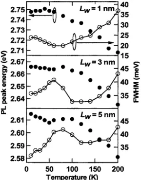
The PL peak energies as a function of temperature are shown in Fig. 5. The magnitude of the S-shape features, i.e., the redshift and the blueshift energies, varies with Lw. This
result is probably related to the degree of localization and also to the densities of the localized sites in each MQW. The MQW with the narrowest thickness 共1 nm兲 exhibits fewer localized sites than the other samples. Thus, the redshift-blueshift-redshift change for this MQW becomes less as tem-perature increases. The dependence of the PL linewidth on temperature was further studied and represented as open circles in Fig. 5, for all of the MQWs. Abnormal evolutions of linewidths were observed at the low temperature. The emission linewidth increased from 10 to 50 K, in which tem-perature range the emission energy was redshifted, in MQW with Lw’s of 3 and 5 nm, as is explained below. The LT
emission band, which simultaneously consists of radiative recombination from free and localized excitons, is broadened by the relaxation of localized excitons to available lower-energy localized states as temperature increases, whereas the free excitons are almost unaffected. This broadening in-creases the PL linewidth and causes a redshift in the peak energy. In the intermediate temperature range from 50 to 100 K, the delocalization effects of trapped excitons overwhelm the reverse relaxation. Therefore, the disappear-ance of the localized excitonic contribution blueshifts the emission energy and reduces the linewidth. At over 100 K, the mobilized excitons radiatively recombine with respect to the temperature-induced band gap shrinkage and interact with phonons, which broaden the transition level. On the other hand, localized states of the 1 nm MQW is limited, from 10 to 50 K, and delocalization simply reduce the re-combination of trapped excitons, narrowing the linewidth of
FIG. 4. Temperature-dependent PL spectra of the Zn0.83Cd0.17Se/ ZnSe MQW with Lw= 5 nm. The close circles indicate the peak energy of the
emission band.
FIG. 5. Evolution of PL peak energy 共close circles兲 and FWHM 共open circles兲 as a function of temperature for the Zn0.83Cd0.17Se/ ZnSe MQWs
with Lw’s of 1, 3, and 5 nm.
063506-4 Ku et al. J. Appl. Phys. 99, 063506共2006兲
the emission band and causing a small blueshift in the peak energy. After 50 K, nearly free excitons dominate the tem-perature dependence of the PL characteristic.
The thermal activation energy is derived from the Arrhenius plot of the integrated PL intensity of the exciton band against the temperature to investigate the thermal quenching of PL in ZnCdSe MQWs grown on a Ge/ Si vir-tual substrate. The high-temperature range of the PL-integrated intensity variations is given by the general equation21
I共T兲 = I共0兲
1 + A exp共− Ea/kBT兲
, 共1兲
where I共T兲 and I共0兲 are the integrated PL intensities at tem-perature T and 0 K, respectively. A is a fitting constant that is related to the ratio of the radiative lifetime to the nonradia-tive lifetime21and kBis the Boltzmann constant. Notably, the
radiative rate is assumed to be constant within temperature in this model. One activation energy Ea was derived for the
temperature range above 120 K. The fitting curves and the values of Eaobtained are shown in Fig. 6. The temperature
dependence of emission intensity in the fitting at LT is ig-nored because the emission band is composed of contribu-tions from both localized and free excitons.
In general, the quenching of PL intensity with tempera-ture can be explained by the thermal emission of the carriers out of a confining potential with an activation energy corre-lated with the depth of the confining potential. The temperature-induced quenching of PL intensity in MQW structures at high temperature is primarily due to the thermal emission of charge carriers out the confined QW states into
barrier states.22The difference between the band gaps of the well and the barrier of this MQW structures is approximately 250 meV.23The confined energies of the conduction and the valence bands are estimated to be in the ranges of 213–163 and 37– 87 meV, considering a band-offset ratio of 0.65–0.85.24 At a high temperature, Ea increases from
44 to 84 meV as Lwincreases. The enhancement of Ea for a
large Lwis presumably due to the decrease of quantized
sub-band energy. This leads to a large energy difference between QW states and barrier states, consequently enlarging the Ea
for thermal emission out of carriers from QW states.
IV. CONCLUSIONS
The deep level emission of ZnSe epilayers grown on the tilted-Ge/ Ge0.95Si0.05/ Ge0.9Si0.1/ Si virtual substrate was
in-vestigated. The PL spectrum of ZnSe epilayers grown on a 6°-tilted Ge/ Si virtual substrate with an inserted LT-MEE layer and an in situ annealed LT-ZnSe buffer layer exhibits the maximum intensity ratio of bound exciton emission to the deep level emission. Quantum-confinement effect of ZnCdSe MQWs grown on a Ge/ Si virtual substrate was identified in the PL spectroscopy. The evolution of exciton emission peak energy and FWHM as a function of tempera-ture suggests lower density of localized states in sample with
Lwof 1 nm. Thermal quenching of excitonic emission
inten-sity for ZnCdSe MQWs grown on Ge/ Si structures was gov-erned by the thermal activation of carriers from QW confined states into barrier states.
ACKNOWLEDGMENT
This work was supported by the National Science Coun-cil of Taiwan under the grant numbers of NSC-93-2112-M-009-031 and NSC94-2112-M-009-013.
1M. A. Haase, J. Qiu, J. M. Depuydt, and H. Chang, Appl. Phys. Lett. 59,
1272共1991兲.
2D. Eason et al., J. Cryst. Growth 150, 718共1995兲.
3R. D. Bringans, D. K. Biegelsen, L. E. Swartz, F. A. Ponce, and J. C.
Tramontana, Phys. Rev. B 45, 13400共1992兲.
4M. K. Lee, M. Y. Yeh, and C. C. Chang, Appl. Phys. Lett. 55, 1850
共1989兲.
5M. Yokoyama, N. T. Chen, and H. Y. Ueng, J. Cryst. Growth 212, 97
共2000兲.
6M. López-López, V. H. Méndez-García, M. Meléndez-Lira, J.
Luyo-Alvarado, M. Tamura, K. Momose, and H. Yonezu, Phys. Status Solidi B
220, 99共2000兲.
7G. L. Luo, T. H. Yang, E. Y. Chang, C. Y. Chang, and K. A. Chao, Jpn. J.
Appl. Phys., Part 2 42, L517共2003兲.
8T. H. Yang, C. S. Yang, G. Luo, W. C. Chou, T. Y. Yang, E. Y. Chang, and
C. Y. Chang, Jpn. J. Appl. Phys., Part 2 43, L811共2004兲.
9J. M. Gaines, J. Petruzzello, and B. Greenberg, J. Appl. Phys. 73, 2835
共1992兲.
10J. S. Song, J. H. Chang, S. K. Hong, M. W. Cho, H. Makino, T. Hanada,
and T. Yao, J. Cryst. Growth 242, 95共2002兲.
11M. C. Kuo et al., Jpn. J. Appl. Phys., Part 2 43, 5145共2004兲.
12U. Lunz, J. Kuhn, F. Goschenhofer, U. Schüssler, S. Eiufeldt, C. R.
Becker, and G. Landwehr, J. Appl. Phys. 80, 6861共1996兲.
13R. Cingolani et al., Phys. Rev. B 51, 5176共1995兲.
14H. J. Lozykowski and V. K. Shastri, J. Appl. Phys. 69, 3235共1991兲. 15M. Godlewski, J. P. Bergman, B. Monemar, E. Kurtz, and D. Hommel,
Appl. Phys. Lett. 69, 2843共1996兲. FIG. 6. Arrhenius plots of the integrated PL intensity vs the inverse of
temperature for the ZnSe/ Zn0.83Cd0.17Se MQWs with Lw’s of 1 nm共open
triangles兲, 3 nm 共open squares兲, and 5 nm 共open circles兲. The solid lines represent the fits to Eq. 共1兲. Derived activation energies Ea’s were also
shown.
16K. Shahzad, J. Petruzzello, D. J. Olega, and D. A. Cammack, Appl. Phys.
Lett. 57, 2452共1990兲.
17C. S. Yang, D. Y. Hong, C. Y. Lin, W. C. Chou, C. S. Ro, W. Y. Uen, W.
H. Lan, and S. L. Tu, J. Appl. Phys. 83, 2555共1998兲.
18X. B. Zhang, K. L. Ha, and S. K. Hark, J. Cryst. Growth 223, 528共2001兲. 19Y. H. Cho, G. H. Gainer, A. J. Fischer, J. J. Song, S. Kreller, U. K. Mishra,
and S. P. DenBaars, Appl. Phys. Lett. 73, 1370共1998兲.
20T. Makino et al., Appl. Phys. Lett. 78, 1979共2001兲.
21M. Leroux, N. Grandjean, M. Laugt, J. Massies, B. Gil, P. Lefebvre, and P.
Bigenward, J. Appl. Phys. 86, 3721共1999兲.
22E. Tournié, C. Morhain, M. Leroux, C. Ongaretto, and J. P. Fourie, Appl.
Phys. Lett. 67, 103共1995兲.
23The band gap energy of ZnSe at a low-temperature limit共0T兲 is 2.82 eV.
Calculate the band gap of ZnxCd1−xSe 共x=0.17兲 using the method
de-scribed in Ref. 12; we get a band offset of 250 meV for 0T.
24R. L. Gunshor and A. V. Nurmikko, II–VI Blue Green Light Emitters: Device Physics and Epitaxial Growth共Academic, Boston, 1997兲, p. 179.
063506-6 Ku et al. J. Appl. Phys. 99, 063506共2006兲