Testable Design and BIST Schemes for FIR Filter Structures
4
0
0
全文
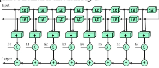
(2) building blocks in the filter. In this paper, we present testable design and built-in self-test schemes for FIR filters. The characteristic of a bijective cell function is used to make the filter array easily testable. According to this approach, pseudoexhaustive test patterns can be applied to each module in the filter and faulty effects can be propagated to the primary outputs. The test pattern generator can be implemented with a simple binary counter and the output response analyzer is implemented with a checksum accumulator. In order to make the filter easily testable, some Design-fortestability techniques should be made. Our approach is also suitable for diagnosis of a faulty module. In order to verify our approach, a cell-based design of the BISTed filter has been implemented. Experimental results show that 100% fault coverage is achieved. The hardware overhead is 7.12% and 5.53% for wordlength = 16 and 24, respectively. The rest of the paper is organized as follows. Section 2 presents the definitions and theories that will be used in this paper. The proposed BIST scheme is presented in Section 3. Experimental results and comparisons are given in Section 4. Finally, conclusions are given in Section 5.. 2. Definitions and Testable Design We assume a cell in an ILA with function f is a combinational machine (Σ, ∆, f), where f: Σ→ ∆ is the cell function, and Σ = ∆ = {0, 1}w, w denotes the word length of a cell. An ILA is an array of cells. Definition: A complete or exhaustive input sequence σ for a cell with function f is an input sequence consisting of all possible input combinations for the cell. A complete output sequence is defined analogously. Definition: A minimal complete (exhaustive) input sequence α for a cell is an input sequence consisting of all possible input combinations for the cell. A minimal complete output sequence β is defined analogously. Definition: We say f is injective if ∀(i1 , j1) (i2 , j2), f (i1 , j1) (i2 , j2). The cell function f is bijective if f is injective andΣ = △. A C-testable array is an array testable with a constant number of test patterns independent of the size of the array. A cell function is x-bijective if f (i1 , j) (i2 , j) if f is x-injective and Σx = △x.. Definition: A feasible complete input sequence for a cell is an input sequence consisting of all possible input combinations for the cell when the primary inputs of the ILA are applied a minimal complete input sequence. Similarly, an unfeasible input sequence for a cell is an impossible input sequence for the cell ({ ∪ } = α). A feasible complete output sequence and an unfeasible output sequence are defined analogously. Our test approach is based on pseudoexhaustive testing at the module level (adder modules and multiplier modules). In other words, applying a feasible complete input sequence to each module in the FIR array. We assume that only one module can be faulty at a time and that only combinational faults can occur.That is, single-module fault model is adopted in this paper. Theorem: A linear phase FIR filter as shown in Fig. 1 is C-testable if the pipeline latches at the second row are made bidirectional. Proof: Controllability: We first examine how to apply all possible input combinations to each module in the filter. From Fig. 1, the pipeline latches at the second row are made bidirectional. In test mode, they propagate patterns from the left to the right. Therefore, if a minimal complete input sequence is applied to the left-most pipeline latches, then this sequence will propagate through the pipeline latches and the adders in the third row will receive the same minimal complete input sequence and generate a feasible complete output sequence. This sequence is then forwarded to the multiplier modules at the fourth row. Since the coefficients for the multiplier modules are directly controllable, the multiplier modules then will receive a feasible complete input sequence. For the adders at the bottom row, their inputs are sent from the pipeline latches, a minimal complete input sequence can be scanned in through the scan chain formed by the pipeline latches. Observability: Apart from applying a minimal (feasible) complete input sequence to all the modules, we must ascertain that all faulty effects propagate toward primary outputs and the faults are observed. According to the fault model adopted, let’s consider all module types and how to propagate faulty effects to the primary outputs. ♦ Adder cells at the third row. If the single faulty module is an adder cell in the third row, its output will be faulty. Since the multiplier modules have an xbijective function, the fault will propagate to the outputs of the multiplier module and then to the primary outputs through the chain of adders at the.
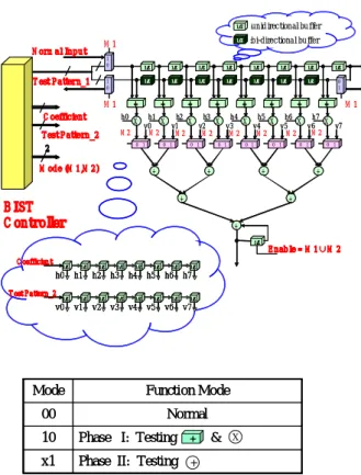
(3) bottom row, following the sum lines). ♦ Multiplier cells at the fourth row. If the single faulty module is a multiplier at the fourth row, Since the outputs drive the chain of adders, faulty effects propagate to the primary outputs (again following the sum line) and thus are detected. ♦ Adder modules in the bottom row. When the fault occurs in one of the adder module at the bottom row, faulty effects propagate to the primary outputs (again following the sum line) and thus are detected.. 3. Built-In Self-Test. M1. N orm al Input. 1 0. T est P attern_1. 1 0. h0. T est P attern_2 2. M2. X. :bi-directionalbuffer. 1/Z. 1/Z. 1/Z. 1/Z. 1/Z. 1/Z. 1/Z. 1/Z. 1/Z. 1/Z. 1/Z. 1/Z. 1/Z. 1/Z. 0 1. +. +. +. +. +. +. +. M1. h1 h3 h4 h5 h6 h7 h2 X X X X X X X v7 v0 v1 v2 v3 v4 v5 v6 M 2 M 2 M2 M 2 M 2 M 2 M 2. 0 1. M ode (M 1,M 2). :unidirectional buffer. 1/Z. 1/Z. +. M1 C oefficient. 1/Z. 0 1. 0 1. +. 0 1. 0 1. 0 1. +. 0 1. +. 0 1. +. described as follows. 3.1 Phase-I BIST mode Phase-I BIST mode is adopted to test the adder modules at the third row and multiplier modules. The filter we discuss here is assumed coefficients-fixed such that test patterns for the coefficient inputs in the multiplier are hardwired. Based on Thm. 1, if all injective adders and multipliers are applied their feasible complete input sequences, they are then well tested. As a result, the BIST controller in our scheme sends the minimal complete input sequences to the inputs of the filter such that all injective adders and multipliers receive their feasible complete input sequences, and are well tested. The accumulator at the last stage of the filter generates a check-sum for the resulted outputs. Fig. 3 shows the filter’s architecture during Phase-I BIST mode. Test_pattern 1 denotes a minimal complete input sequence sent from the controller. 0. +. B IST C ontroller. +. T est Pattern_1 +. 0 1. 1/Z. E nable = M 1∪M 2 C oefficien t. 1/Z. h0 T est P attern _2. 1/Z. v0. 1/Z. h1 1/Z. v1. 1/Z. h2 1/Z. v2. 1/Z. h3 1/Z. v3. 1/Z. h4 1/Z. v4. 1/Z. h5 1/Z. v5. 1/Z. h6 1/Z. v6. 1 0. 0. 0. 0. 0. 0. 0. 0. 0. 6. 5. 4. 3. 2. 1. 0. +. +. +. +. +. +. 1/Z 1 0. +. +. 0. 1/Z. h0 X. h7. 0. 1/Z. v7. h1 X h2 X h3 X h4 X h5 X h6 X h7 X v0 v1 v2 v3 v4 v5 v6 v7. 0 1. 0. 0 1. 0. +. 0 1. 0. 0 1. 0. 0 1. +. Function Mode. 00. Normal. 10. Phase I: Testing. +. x1. Phase II: Testing. +. 0 1. 0. +. +. Mode. 0. 0 1. 0. 0 1. + +. + 1/Z. &. E nab le = 1. X. Fig. 2: Architecture of the BIST-based FIR filter. In Fig. 2, we show the architecture of the proposed BIST-based FIR filter, which consists of the BIST controller and the testable design of the FIR filter described above. The adders at the bottom row are treeconnected. In other words, the FIR filter performs a series of additions in a sequential fashion to obtain the final output. The performance of the filter can be significantly improved by executing some of these additions in parallel, as the tree of adders in Fig. 2 [5]. The BIST controller coordinates the testing procedures and the generation of test patterns. The filter has three operating modes—Normal mode, Phase-I BIST mode and Phase-II BIST mode. When the filter operates in Normal mode, multiplexers are set to make the filter work as Fig. 1. The BIST modes of the filter are. Fig. 3: The FIR filter in Phase-I BIST mode. 3.2 Phase-II BIST mode Phase-II BIST mode is adopted to test the tree of adders in the FIR filter. Based on Thm. 1, if all injective adders in the tree are applied their feasible complete input sequences, they are then well tested. The BIST controller in our scheme sends the minimal complete input sequences to the inputs of the adder tree such that all injective adders receive their feasible complete input sequences and are well tested. Fig. 4 shows the FIR filter’s architecture during Phase-II BIST mode. In this figure, Test Pattern_2 denotes a minimal complete input sequence comes from the BIST controller. The blocks at the top row in the figure denote pipeline latches. The adder at the bottom row acts as a accumulator to calculate the checksum of the resulted outputs. The final checksum in the adder is.
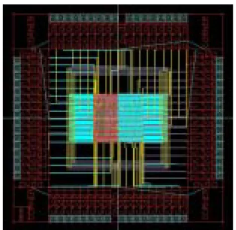
(4) Table 1: Hardware overhead of the BISTed FIR filter.. sent to the controller to make the pass/fail decision. T est Pattern_2 7. 6. v0 1. 0 1. 5. v1 1. 0 1. 4. v2 1. +. 0 1. 3. v3 1. 0 1. 2. v4 1. 0 1. +. 1. v5 1. v6. 0 1. 1. Wordlength Length 16 24 32. 0. 0 1. +. v7 1. 0 1. Hardware Overhead 7.12% 5.53% 4.43%. +. 5. Conclusions +. +. + 1/Z. E nable = 1. Fig. 4. Phase-II BIST mode. In our BIST scheme, test patterns are simply generated by a binary counter. It helps a lot to reduce the hardware overhead for the BIST design. Furthermore, feasible complete input sequence is used to test the FIR filer, which saves much unnecessary simulation time caused by unfeasible input sequences.. 4. Experimental Results and Comparisons In order to verify our approach, a cell-based experimental chip is implemented with Synopsys tools. The chip layout is shown in Fig. 5 and all the BIST modes have been verified. The chip size is about 2.3 × 2.3 mm2. The hardware overhead of our approach is shown in Table 1. From this table, it is obvious that the hardware overhead decreases as the wordlength increases. The simulation time to test the first stage adders and multipliers of FIR filter in our scheme is only a half of [5]’s. The simulation time to test the tree of adders is 8 times faster as compared with [5]’s. Moreover, the test patterns used in [5] are generated by an arithmetic additive generator. It will cause larger hardware overhead to implement the BIST structure.. This paper presents testable design and built-in self-test schemes for digital finite impulse response (FIR) filters. According to the characteristics of a bijective cell function, feasible (minimal) complete test patterns can be applied to each module in the filter and faulty effects can be propagated to the primary outputs. The test pattern generator can be implemented with a simple binary counter. We use the checksum approach for output response analysis. In order to verify our approach, a cell-based design of the BISTed filter has been implemented. Experimental results show that 100% fault coverage is achieved. The hardware overhead is 7.12% and 5.53% for wordlength = 16 and 24, respectively. These results show that our BIST scheme is more efficient than the external testing method proposed in [5]. The hardware overhead is also less then that in [5]. Reference [1] [2]. [3]. [4]. [5]. [6]. [7]. [8]. Fig. 5: The chip layout of the BISTed FIR filter.. R. J. Higgins, Digital Signal Processing in VLSI. Prentice Hall, 1990. E. C. Ifeachor and B. W. Jervis, Digital Signal Processing/ A Practical Approach. Addisin-Wesley, 1993. H. Fujiwara and S. Toida, “The complexity of fault detection problems for combinational logic circuits,” IEEE Trans. Computers, vol. C-31, pp. 555-560, June 1982. Laurence Goodby and Alex Orailoglu, “Towards 100% Testable FIR Digital Filters,” Proc. Int’l Test Conference, pp. 394-402, 1995. N. Technologies, J. Rajski, and J. Tyszer, “Parameterizable Testing Scheme for FIR Filters,” Proc. Int’l Test Conference, pp. 694-703, 1997. N. Technologies, J. Rajski, and J. Tyszer, “Testing Schemes for FIR Filter Structures,” IEEE Trans. Computers, vol. 50, no. 7, pp. 674-688, July, 2001. S. Gupta, J. Rajski, and J. Tyszer, “Arithmetic Additive Generators of Pseudo-Exhaustive Test Patterns,” IEEE Trans. Computers, vol. 45, no. 8, pp. 939-949, August, 1996. C. W. Wu and P. R. Cappello, “Easily Testable Iterative Logic Arrays,” IEEE Trans. Computers, vol. 39, pp. 640-652, May 1990..
(5)
數據
相關文件
• Implied volatility (IV) is the volatility input in a pricing model that, in conjunction with the other four inputs, returns the theoretical value of an option matching the
[ Composite ] → Tree [ Composite ] receives a significance order of fields and classifies the input list first by the most significant field, and for each bucket classifies the
Making use of the Learning Progression Framework (LPF) for Reading in the design of post- reading activities to help students develop reading skills and strategies that support their
The research proposes a data oriented approach for choosing the type of clustering algorithms and a new cluster validity index for choosing their input parameters.. The
The temperature angular power spectrum of the primary CMB from Planck, showing a precise measurement of seven acoustic peaks, that are well fit by a simple six-parameter
The design of a sequential circuit with flip-flops other than the D type flip-flop is complicated by the fact that the input equations for the circuit must be derived indirectly
To complete the “plumbing” of associating our vertex data with variables in our shader programs, you need to tell WebGL where in our buffer object to find the vertex data, and
Microphone and 600 ohm line conduits shall be mechanically and electrically connected to receptacle boxes and electrically grounded to the audio system ground point.. Lines in
![TraditionalMLCalgorithmsmainlytacklethebatchMLCproblem,wheretheinputdataarepresentedinabatch[24,28].Nevertheless,inmanyMLCapplicationssuchase-mailcategorization[22],multi-labelexamplesarriveasastream.Onlineanalysisistherefore dimensionreducermotivatedbyma](data:image/gif;base64,R0lGODlhAQABAIAAAP///wAAACH5BAEAAAAALAAAAAABAAEAAAICRAEAOw==)