I-Shou University Institutional Repository:Item 987654321/18631
80
0
0
全文
(2) 添加玻璃粉末對氧化錫燒結和 性質之影響 The Effects of Doping Glass Powder on Sintering and Properties SnO2 研 究 生 : 孫 宸 楷 Student :Sun Cheng Kai . . . . . . . . 指導教授:洪博彥. . Advisor:Boen Houng . 義 守 大 學 材料科學與工程學系 碩士論文 A Thesis Submitted to Department of Materials Science & Engineering I-Shou University in Partial Fulfillment of the Requirements for the Master degree in Materials Science & Engineering July, 2015 Kaohsiung, Taiwan, Republic of China. 中 華 民 國 104 年 7 月 .
(3)
(4) 添加玻璃粉末對氧化錫燒結和 性質之影響 摘. 要. 利用 GeO2, MoO3 及 V2O5 所組成的獨特玻璃可作為助燒劑來增加 SnO2 陶瓷緻密化及改善其電性能。此法可使燒結溫度降低至 950℃左 右,並得到優異的電性能。此研究利用金屬氧化玻璃的濃度來改善 SnO2 陶瓷的緻密化及電性能,主要有運用阿基米得原理、XRD 及 SEM 來完 成其研究。此種玻璃的添加能夠不改變 SnO2 陶瓷的晶體結構,且能改 善 SnO2 陶瓷的緻密化效率及晶粒尺寸。 添加此種玻璃亦能在較低溫下,形成一層很薄連續液相及促進 SnO2 顆粒重排成較緊密結構。利用熱壓的方式也能協助 SnO2 的緻密化 效率,使得產生相對較小的晶粒尺寸與較緊密的結構。SnO2 陶瓷的電性 能特性在玻璃摻雜其中時而有所改變。在高濃度玻璃摻雜其中,可能會 在晶界周圍形成非晶相,這樣會抑制晶粒成長過快同時對 SnO2 陶瓷的 電化性亦扮演一個重要關鍵角色。而未來研究方向則著重在鑑定晶界及 SnO2 晶粒的化學組成。 關鍵字:氧化錫、緻密化、金屬氧化玻璃。. I.
(5) Abstract A unique glass composition based on GeO2, MoO3 and V2O5 was designed to act as sintering aid to enhance the densification and to adjust the electrical properties of SnO2. This allows the low temperature processing of approximately 950 ◦C to be feasible with a desirable electrical property. The effect of metal oxide glass concentration on the densification behavior and electrical properties of SnO2 was investigated by Archimedes' principle, x-ray diffractometer (XRD), scanning electron microscopy (SEM) techniques. The addition of glass was found not to affect the crystal structure of SnO2, but it increased the densification rate and the grain size of SnO2. The glass additive formed a thin continuous liquid phase and rearranged SnO2 particles into a dense microstructure at much low temperature. Applying the external press during hot pressing also assisted the densification rate of SnO2 and resulted in a relatively small grain size and denser microstructure. The electrical properties of were found to affect by the microstructure of glass doped SnO2 ceramics. At higher glass concentration doping, the possible formation amorphous phase around at grain boundary played a key role on the electrical properties of SnO2 ceramics. Further work on the identification of grain boundary phase is. II.
(6) needed to perform as well as chemical composition of SnO2 grains.. keywords:SnO2、densification、Metal oxide glass.. III.
(7) 致. 謝. 在面對即將口試的日子裡,想起剛進入碩士班的那一刻,從以前的大班制變成 小班制時,上課時不由自主認真了起來,才真正體會這就是碩士班的課程,這幾年 裡經歷公司的調動、派駐大陸期間,一度放棄碩士學業的我,在洪老師的極力配合 下,讓我的碩士論文燃起完成的機會。 謝謝洪老師的協助,讓我在碩士學習期間,少走了一些冤枉路,給於我很多實 質的建議和寶貴的經驗,在剛開始毫無頭緒的情況下,慢慢的指引出一個方向,也 謝謝碩士班學弟們的配合,協助我將論文的架構,逐漸完善起來,並給於實際的行 動,讓在公司忙得焦頭爛額的我,在完成碩士學業的過程中,可以在兩方面進度和 事情處理的下,達到妥當的平衡。 謝謝幫我的人,在未來的日子裡,無論學界、產業上的需求,任何在可幫忙的 情況下,小弟我一定竭盡所能,讓曾經幫助過我的人,接受我的回報,另外,謝謝 兩位老師在百忙之中暑假期間,過來聆聽學生的論文口試,並給於適時的指導,在 往後的學習道路上,有了更明確的方向。 最後,感謝所有人(公司同仁、學弟妹們),還有最辛苦的指導老師 洪博彥老師, 沒有你的辛苦指導,給於極大的幫忙,學生也無法完成艱鉅的碩士學業,所以特別 謝謝你,在碩士學業上感謝有你。 孫宸楷 謹致於義守大學材料系 2015 年 07 月 24 日 . IV.
(8) 總 目 錄 中文摘要 .............................................................................................................. Ⅰ 英文摘要 .............................................................................................................. Ⅱ 致謝 ...................................................................................................................... Ⅳ 總目錄 .................................................................................................................. Ⅴ 表目錄 .................................................................................................................. Ⅶ 圖目錄 .................................................................................................................. Ⅷ 1.Introduction and objective ................................................................................... 1 1.1 Objective of this work .................................................................................. 2 2.Basics and literature survey ................................................................................. 5 2.1 Properties and Application of SnO2 .............................................................. 6 2.1.1 Opaque Glass ......................................................................................... 7 2.1.2 Granite and Marble Polishing................................................................ 7 2.1.3 Glass coatings ........................................................................................ 8 2.1.4 Gas sensing ............................................................................................ 8 2.2 Sintering theory............................................................................................. 9 2.2.1 Sintering mechanisms.......................................................................... 10 2.2.2 The stages of sintering ......................................................................... 13 2.3 The liquid phase sintering........................................................................... 16 2.4 Literature review of sintering of SnO2........................................................ 19 3.Experimental procedure..................................................................................... 29 3.1 Oxide glass preparation .............................................................................. 29 3.2 SnO2 ceramic preparation ........................................................................... 29 3.3 Archimedes’ Principle and Density Determination .................................... 30. V.
(9) 3.4 The principal of scanning electron microscopy.......................................... 32 3.5 The principal of X-ray diffraction .............................................................. 36 4.Results and discussions...................................................................................... 40 4.1 Shrinkage behavior ..................................................................................... 40 4.2 Structure analysis........................................................................................ 42 4.3 Electrical properties evaluation .................................................................. 52 4.4 Summary..................................................................................................... 63 5.Further work ...................................................................................................... 65 6.Reference ........................................................................................................... 66. VI.
(10) 表 目 錄 Table 2.1 Chemical and physical properties of SnO2 ceramics .............................. 6 Table 2.2 Different transport mechanisms during sintering processing ............... 11 Table 4.1 Density of glass doped SnO2 ceramics ................................................. 41 Table 4.2 The grain size (D) and (ε) values of doped SnO2 ceramics .................. 47. VII.
(11) 圖 目 錄 Fig. 2.1 3D model for SnO2 structure. Red atoms are tin atoms ............................ 5 Fig. 2.2 Alternate path ways of atoms diffusion according to the Table 2.2 ........ 12 Fig. 2.3 Stages of sintering. (a) initial stage, (b)near end of initial stage, (c) intermediate stage and (d) final stage................................................. 14 Fig. 2.4 FESEM photograph for a sample during an initial sintering stage ......... 15 Fig. 2.5 Three stages of a sample during a liquid phase sintering process........... 18 Fig. 2.6 Microstructure development during a liquid phase sintering.................. 18 Fig. 2.7 Oxygen partial pressure as a function of temperature............................. 20 Fig. 2.8 The grain size (GBET) and crystallite size (GXRD) of SnO2 as a function of temperature ........................................................................... 22 Fig. 2.9 SEM micrographs of fractured samples with ZnO content of 0.5 mol %, (b) 1.0 mol % and (c) 5 mol % ZnO..................................... 23 Fig.2.10 Scanning electron microscopy micrographs of SnO2before and after exposure to 80 V cm−1at 900◦C (a–c), 1100◦C (d–f) and 1300◦C (g–i). Limitingcurrent: 1 A (b, e, h); 5 A (c, f, i).Images taken at the top fracture center of the samples ................................................. 25 Fig.2.11 Dielectric constant versus frequency curves of SnO2 samples with different additives................................................................................... 26 Fig.2.12 SEM micrographs for SZC system doped with: (a) 0.05 mol% of Ta2O5 and (b) 0.075 mol% Ta ................................................................ 27 Fig.2.13 SEM images of furnace-sintered and APPJ sintered nanoporous SnO2 . 28 Fig.3-1 Example of Archimedes' Principle to determine the density of sample............................................................................................... 31. VIII.
(12) Fig. 3.2 Schematic drawing of the scanning electron microscopy structure ..... 35 Fig. 3.3 An example of scanning electron microscopy machine....................... 36 Fig. 3.4 An example of X-ray diffractometer. ................................................... 38 Fig. 3.5 An X-ray diffraction pattern of an unknown sample ........................... 39 Fig. 4.1 Density of glass doped SnO2 ceramics as a function of sintered temperature at different doping concentrations. .................................. 41 Fig. 4-2 XRD patterns of SnO2 ceramics doped with 1, 3 and 5 wt % glass sintered at 800°C ................................................................................. 43 Fig. 4-3 XRD patterns of SnO2 ceramics doped with 1, 3,5 and 10 wt % glass sintered at 900°C. ................................................................................ 43 Fig. 4-4 XRD patterns of SnO2 ceramics doped with 1, 3, 5 and 10 wt %glass sintered at 950°C. ................................................................................ 44 Fig. 4-5 The grain size of doped SnO2 ceramics sintered 800, 900 and 950°C for different doping concentrations. ................................................... 45 Fig. 4-6 The strain of doped SnO2 ceramics sintered 800, 900 and 950°C for different doping concentrations. .......................................................... 46 Fig. 4.7 SEM cross-section images of 1 wt % glass doped SnO2 ceramics sintered at 800, 900 and 950°C............................................................ 49 Fig. 4.8 SEM cross-section images of 3 wt % glass doped SnO2 ceramics sintered at 800, 900 and 950°C............................................................ 50 Fig. 4.9 SEM cross-section images of 5 wt % glass doped SnO2 ceramics sintered at 800, 900 and 950°C............................................................ 50 Fig. 4.10 SEM cross-section images of 10 wt % glass doped SnO2 ceramics sintered at 900 and 950°C. .................................................................. 51. IX.
(13) Fig. 4.11 Capacitance of 1 wt % glass doped SnO2 ceramics sintered at different temperatures........................................................................ 53 Fig. 4.12 Capacitance of 3 wt % glass doped SnO2 ceramics sintered at different temperatures. ...................................................................... 54 Fig. 4.13 Capacitance of 5 wt % glass doped SnO2 ceramics sintered at different temperatures. ...................................................................... 55 Fig. 4.14 Capacitance of 10 wt % glass doped SnO2 ceramics sintered at different temperatures. ...................................................................... 56 Fig. 4.15 Electrical resistivity of 1 wt % glass doped SnO2 ceramics sintered at different temperatures. ........................................................ 58 Fig. 4.16 Electrical resistivity of 3 wt % glass doped SnO2 ceramics sintered at different temperatures. ........................................................ 60 Fig. 4.17 Electrical resistivity of 5 wt % glass doped SnO2 ceramics sintered at different temperatures. ........................................................ 61 Fig. 4.18 Electrical resistivity of 10 wt % glass doped SnO2 ceramics sintered at different temperatures. ........................................................ 62. X.
(14) 1. Introduction and objective SnO2 polycrystalline ceramics are n-type semiconductors that have been widely used as gas sensors, as electrodes for electric glass melting furnaces and, in thin films, as electrochromic devices, crystal displays, photodetectors, solar cells and protective coatings. However, the use of SnO2 ceramics is limited by the low densification of this oxide during sintering because of the dominance of non-densifying mechanisms for mass transport such as surface diffusion or evaporation-condensation. The high density of SnO2 ceramics can be obtained by hot isostatic pressing (HIP) or with the help of an additive like MnO2, CuO, Li2CO3, ZnO, Nb2O5, Fe2O3 or Co2O3.These oxides serve as sintering aid that assist SnO2 ceramics to densify at a lower sintering temperature.Although in the solid state sintering, densification can be enhanced by the formation of defects due to the dissolution of additive derived species and oxygen vacancies in the SnO2 network. However, SnO2 ceramics are very sensitive to the atmosphere, the interaction of gases with the SnO2 surface promotes charge transfer and defects creation during sintering of this oxide. As a result, larger grains of SnO2 microstructure will present as well as larger pores. This is not ideal microstructure for many applications. For liquid phase sintering of SnO2 ceramics by addition with low melting oxides, the SnO2 solid grains are soluble in the liquid. This solubility causes the liquid to wet the SnO2 solid, providing a capillary force that pulls the grains together. At the same time, the high temperature softens the solid, further assisting densification. High-diffusion rates are also associated with liquids, giving fast sintering or lower sintering temperatures.. 1.
(15) 1.1 Objective of this work SnO2, tin dioxide, shows specific optical and electrical properties and a good chemical stability. Tin dioxide (SnO2) in its pure form is n-type semiconductor and belongs to the important class of transparent conductor oxide materials that combine low electrical resistance with high optical transparency in the visible range of spectrum. These properties are required for optoelectronic applications such as light emitting diodes, electrode materials in solar cells flat panel displays, transparent field effect transistors. Tin dioxide is also an oxidation catalyst and its activity and selectivity can be substantially improved by incorporation of various additives. Another application in which tin dioxide plays a dominant role is gas sensors. A wide variety of oxides exhibit sensitivity as exposing in an oxidizing and reducing environment by a variation of their electrical properties, but SnO2 was one of the most frequently used material for these applications. In addition, SnO2 also be considered as excellent candidate transparent conducting oxide because of its excellent electrical and optical properties. Therefore, increasing attention is being paid to studies on this oxide, especially on the methods of preparation, and its electrical and optical properties. High density in polycrystalline SnO2 ceramics is essential for high performance of these applications, especially for TCO application, since the phenomena involved for high concentration of free electron transport properties occur in the materials. The main limit in a wider use of this type of material is related to poor sintering ability of the SnO2-based targets. The low diffusivity of. 2.
(16) the SnO2 structure and predominance of the non-densifying mechanisms such as surface diffusion and evaporation-condensation were attributed to this behavior. As a result, the grain and pore growth were dominated and thus limited the final density. The sintering problem can be further complicated by presence of high vapor pressure of SnO and the formation of deleterious intermediate phases above 1273K. However, dense SnO2-based ceramics became feasible by the addition of densifying agents such as CuO, CoO, In2O3, Fe2O3, Cr2O3, TiO2, MnO2, MoO3 and ZnO to promote densification of SnO2 ceramics. The objective of this work is to investigate the densification behavior of SnO2 ceramics and their electrical property by two folds. The first approach is to understand the addition of densification agent of glass powder containing GeO2, MoO3 and V2O5 as sintering aid. The second approach is to increase the densification by applied an external pressure during sintering. The low melting point of glass sintering aid provides liquid phase sintering mechanism combining with applied pressure to further improve the densification of SnO2 ceramics. The driving force for liquid phase sintering is derived from the capillary pressure of the liquid phase located between the fine solid particles. Applying a liquid- phase sintering process, refractory ceramics can be sintered at lower temperature by forming thin continuous or semicontinuous liquid phases at grain boundaries. During sintering, the ceramic particles are soluble in the liquid. This solubility causes the liquid to wet the solid, leading a capillary force that pulls the particles together. At the same time, the high temperatures often the solids further promoting densification. High-diffusion rates are also associated with liquids, resulting in fasts sintering or lower sintering temperatures.. 3.
(17) The sintering processes involved an external pressure is also desirable in that it eliminates the need for very fine SnO2 particles and also removes large pores caused by non-uniform mixing. An additional advantage is that densification can be obtained at a temperature at which extensive grain growth and presence of high vapor pressure of SnO do not occur. The effect of sintering temperature and amount of sintering aid on the densification behavior and electrical properties of SnO2 ceramics will be investigated in this study.. 4.
(18) 2. Basics and literature survey It is known that tin dioxide SnO2has a tetragonal rutile crystalline structure (known in its mineral form as cassiterite. The unit cellconsists of two metal atoms and four oxygen atoms. Each metal atom is situated amidst six oxygen atoms which approximately form the corners of a regular octahedron as seen from Fig 2-1. Oxygen atoms are surrounded by three tin atoms which approximate the corners of an equilateral triangle. The lattice parameters are a= 4.7382 Å, and c= 3.1871 Å [1].. Fig.2.1 3D model for SnO2 structure. Red atoms are tin atoms [1].. 5.
(19) 2.1 Properties and Application of SnO2 The chemical and physical properties of SnO2are listed in Table 2.1 [2]. Table 2.1 Chemical and physical properties of SnO2 ceramics[2] Chemical Data Chemical symbol. SnO2. CAS No. 18282-10-5 Tin 14. Group. Oxygen 16. Electronic. Tin [Kr] 4d10 5s2 5p2. configuration. Oxygen [He] 2s2 2p4. Chemical Composition Element. Content (%). Tin. 78.76. Oxygen. 21.21. Properties Metric Density. Imperial 3. 6.95 g/cm. Molar Mass 150.71 g/mol. 0.251 lb/in3 -. Properties Metric. Imperial. Melting Point. 2955°F. 1630°C. 6.
(20) Boiling Point. 1800-1900°C. 3272-3452°F. Tin oxide is an inorganic compound consisting of tin and oxygen. It has been extensively applied in a various fields such as transparent electron devices, p-type thin film transistor, optoelectronic devices, solar cell, flat panel display and gas sensors. In traditional ceramic applications, it is commonly used to create customized glass by giving transparent glass an opaque, porcelain-like, opaque appearance.. 2.1.1 Opaque Glass As applied to glass (using the appropriate amount and technique), tin oxide will completely permeate the glass and interact with the other chemical compounds within the glass that it will turn it from transparent to an opaque white. As a result, the product often called milk glass, which is a design element in many residential and commercial spaces. The same properties have led to the use of tin oxide in fabricating the white glaze that covers on faience, a type of earthenware that has the appearance of white porcelain.. 2.1.2 Granite and Marble Polishing Tin oxide can be used as a highly effective polishing material for glass and quarried rock, such as marble, granite and quartz. When reacts with glass, tin oxide restores the luster of a stone surface--especially marble flooring--that's become dull over time. This technique for polishing is relatively simply: Apply tin. 7.
(21) oxide to the surface with a damp cloth and continuously rub and polish the surface until you achieve the desired sheen.. 2.1.3 Glass coatings SnO2 thin films can be produced by using chemical vapor deposition, vapor deposition techniques that SnCl4 or organo tin trihalides e.g. butyltin trichloride were employed as the volatile agent. This technique is used to coat glass bottles with a thin (<0.1 μm) layer of SnO2, which helps to adhere a subsequent, protective polymer coating such as polyethylene to the glass. Thicker films doped with F or Sb ions are electrically conducting and used in electroluminescent devices.. 2.1.4 Gas sensing SnO2 also are commonly used as the detecting element to detect the combustible gases such as carbon monoxide. Within these the sensor, the surface area is heated to a constant temperature (few hundred °C) and in the presence of a combustible gas the electrical resistivity changes. Doping with various compounds has been investigated to improve the sensitivity of sensor (e.g. with CuO). Doping with other oxides such as cobalt and manganese, gives the sample that can be used in high voltage varistors. SnO2 can also be doped with the oxides of iron or manganese for different purposes.. 8.
(22) 2.2 Sintering theory Sintering is an important heat processing during ceramic forming. Sintering can be described an operation that involves a heating treatment with or without the application of external pressure in which particles are attached into a coherent body. The main driving force is the reduction of surface area, which can be achieved by solid state reactions or alternatively in the presence of a liquid phase. The driving force for densification is the change in free energy by decreasing in surface area and lowering of the surface free energy by changing to a solid-vapor interface. As a result, it forms new but lower-energy solid-solid interfaces with a lower free energy. In practice, sintering is the control of both densification and grain growth. The densification is the act of reduction of the porosity in a sample thereby making it more a dense body. Whereas, grain growth is the process of grain boundary motion and Ostwald ripening to increase the average grain size. Many properties (mechanical strength, electrical breakdown strength, etc.) benefit from both a high relative density and a small grain size. Therefore, whether able to control of these properties during processing is of high technical importance. Since densification of powders requires high temperatures, grain growth naturally occurs during sintering [3].. 9.
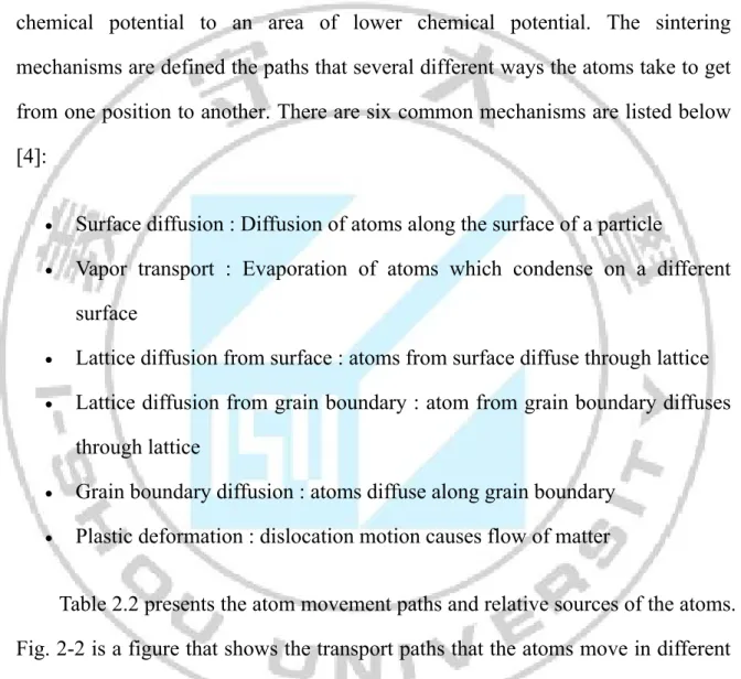
(23) 2.2.1 Sintering mechanisms Sintering is a heat process that involves the diffusion of atoms through the microstructure. A gradient of chemical potential in the sample will cause the diffusion of atoms to occur. The diffusive atoms move from an area of higher chemical potential to an area of lower chemical potential. The sintering mechanisms are defined the paths that several different ways the atoms take to get from one position to another. There are six common mechanisms are listed below [4]: . Surface diffusion : Diffusion of atoms along the surface of a particle. . Vapor transport : Evaporation of atoms which condense on a different surface. . Lattice diffusion from surface : atoms from surface diffuse through lattice. . Lattice diffusion from grain boundary : atom from grain boundary diffuses through lattice. . Grain boundary diffusion : atoms diffuse along grain boundary. . Plastic deformation : dislocation motion causes flow of matter Table 2.2 presents the atom movement paths and relative sources of the atoms.. Fig. 2-2 is a figure that shows the transport paths that the atoms move in different ways during sintering stages.. 10.
(24) Table 2.2 Different transport mechanisms during sintering processing [4]. 11.
(25) Fig. 2.2 Alternate path ways of atoms diffusion according to the Table 2.2 [4].. In general, it is necessary to distinguish between densifying and non-densifying mechanisms. For 1–3 on the listed above Table are non-densifying mechanisms. The atoms leave from the surface and rearrange them onto another surface or part of the same surface. These mechanisms simply rearrange matter inside of porosity and do not cause pores to shrink. For densifying mechanisms, 4-6 mechanisms listed in above Table which atoms are moved from the bulk to the surface of pores thereby eliminating porosity and increasing the density of the sample.. 12.
(26) 2.2.2 The stages of sintering In general, the above list of observations has been used to classify three stages in the overall sintering process within which to build models: 1.. Initial stage: In this stage, a collection of particles of a single phase the dihedral angle usually is high and therefore points of contact between particles will grow into necks if some mechanism is available to allow the equilibrium geometry to be reached.. 2.. Intermediate stage: During this stage, the porosity in the sample is reduced to about 15 %. The grin boundary energy begins to play a significant contribution to the total energy of the system and the grain boundaries begin to rearrange themselves to minimize their total area. In this stage of sintering, the geometry thus becomes that of an assembly of polyhedral grains with pore along the three grain edges, and the tendency to minimize the grain boundary area results in grain growth.. 3.. Final stage: In this stage, the pores continue to shrink as sintering proceeds and they become isolated pores at four grain corners. The stage commences at 5 % total porosity and may continue until all porosity is eliminated. Fig. 2.3 is a model to develop three sintering stages. Fig 2.4 is a FESEM photograph of a sintered sample shown a neck growth during an intermediate stage of sintering.. 13.
(27) Fig.2.3 Stages of sintering. (a) initial stage, (b)near end of initial stage, (c) intermediate stage and (d) final stage [4].. 14.
(28) Fig 2.4 FESEM photograph for a sample during an initial sintering stage [5].. For improving properties such as thermal and electrical conductivity, translucency and strength it is desirable to eliminate as much of the porosity as possible. For some other application it may be desirable to increase the strength without decreasing the gas permeability. Therefore, the conventional ceramic method, the hot isostatic pressing technique and spark plasma sintering technique are some of the techniques used for the obtaining sintered compacts. In addition, liquid phase sintering is also an effective method to improve the densification of ceramics at a much more lower sintering temperature.. 15.
(29) 2.3 The liquid phase sintering As the grain boundary impurity phases can be tolerated, and the ceramic artefact is not to be chosen for its high temperature strength properties, then this method of sintering is attractive because the densification kinetics are much more rapid than in solid state sintering. There two variants of liquid phase sintering depending on how the liquid phase exists during the isothermal sintering time: (a)whenthe sintering temperature is reached, the liquid phase start to appear, and remains until cooling takes place and causes it to solidify. As a result, a heterogeneous system will present and implies only a limited solubility of the liquid in the matrix. (b) As the liquid phase appears at the sinter temperature, andit gradually disappears due to soluble in the matrix phase. This produces homogeneous sinters equivalent to some forms of solid state sinter. The three stages in liquid phase sintering are plottedin Fig. 2.5 where they are defined relative to the densification curve [6]. 1.Rearrangement: As the liquid melts, capillary force will pull the liquid into pores and also cause grains to rearrange into a more favorable packing arrangement. 2.Solution-Precipitation: The place where the areas their capillary pressures are high(particles are close together), the atoms will preferentially go into solution and then precipitate in areas of lower chemical potential. The particles are not close or in contact. This is generally called "contact flattening". This densification mechanism in the system is similar to grain. 16.
(30) boundary diffusion in solid state sintering. In this stage, oswald ripening will also occur where smaller particles will go into solution preferentially and precipitate on larger particles leading to densification. 3.Final Densification: In this stage, densification further develops a solid skeletal network, liquid movement from efficiently packed regions into pores. For liquid phase sintering to be practical the major phase should be at least slightly soluble in the liquid phase and the additive should melt before any major sintering of the solid particulate network occurs, otherwise rearrangement of grains will not occur. Fig. 2.5 shows three stages of liquid phase sintering as sintering time is developed. Fig 2.6 presents a microstructure development during liquid phase sintering [7].. 17.
(31) Fig 2.5 Three stages of a sample during a liquid phase sintering process [7].. 18.
(32) Fig 2.6 Microstructure development during a liquid phase sintering [7].. 2.4 Literature review of sintering of SnO2 Pure tin dioxide is an n-type semiconductor with tetragonal crystalline structure similar to that of rutile. SnO2 has many uses such as in gas sensors, electrodes for electric glass melting furnaces, electro chromic devices, crystal displays, photo detectors, solar cells and protective coatings. However, the use of tin dioxide ceramics is limited due to poor densification during sintering caused by the dominance of non-densifying mechanisms for mass transport such as surface diffusion or evaporation condensation. These mechanisms promote grain coarsening of SnO2 leading to poor densification of this ceramics.. To explain the predominance of the non-densifying mechanism during the sintering process of SnO2 powder, several models have been proposed. Varela et al. and Kimura et al [8] proposed a mechanism based on an evaporation /condensation process to explain the grain growth process during the sintering of SnO2 powder, in a temperature range of 1000 – 1400 oC.In both work, no macroscopic shrinkage was observed. Therefore, analysis of the SnO2 evaporation process is therefore of fundamental importance. To understand the sintering mechanism, Hoenig et al [9] studied the evaporation process of SnO2 and reported that at high temperatures this oxide showed a peritectic decomposition according to the reaction: SnO2 --SnO +1/2 O2. 19. (1).
(33) In the temperature range 1200 to 1700 K, the oxygen partial pressure is given by:. logPO2 (atm) = -2.061 x10 -4/T +8.656. (2). where PO2 is the oxygen partial pressure and T the temperature. Considering above equation, in Fig. 2.7, a substantial increase of PO2 is observed for temperature higher than 1200 oC, which suggests a high evaporation rate for these temperatures. Even using ultrafine SnO2 powder, a full density of SnO2 ceramic is still not achieved. The experiments have been conducted by using sol-gel derived SnO2 powders to study the sintering process of ultrafine SnO2 powders, in the temperature range 400 to 1500 oC. The results showed that the mass transport mechanism is controlled by surface diffusion at low temperature from 500 to 1000 o. C. Whereas, the mass transport mechanism is controlled by evaporation. -condensation at temperature greater 1300 oC.. 20.
(34) Fig 2.7 Oxygen partial pressure as a function of temperature [ 9]. Recently, Shi et al. [10] have analyzed the importance of surface diffusion on densification during the sintering process and proposed that surface diffusion is the most probable mass transport mechanism to promote particle coarsening and center approaching between particles or grains.. E. R. Leite et al [11] had used pure SnO2 to study the densification behavior by constant heating rate and isothermal sintering. Pore size distribution measurements, using gas desorption, and grain size and crystallite size measurements of isothermally sintered samples showed no formation of non-densifying microstructures during the sintering process. Fig. 2.8 showed the grain size and crystallite size of SnO2 as a function of temperature. These results are a strong indication that densification was prevented by thermodynamic factors, mainly the high ratio of GB/SV. An explanation, based on the nature of covalent bonding and the balance between attractive and repulsive forces, was proposed to explain the high GB/SV ratio in SnO2.. 21.
(35) Fig. 2.8 The grain size (GBET) and crystallite size (GXRD) of SnO2 as a function of temperature [11].. Maitre et al [12] has studied the effect of ZrO2 additions on sintering of SnO2-based ceramics. It concluded that the zirconia additions limited the densification of the SnO2-based materials. This effect can be imputed to the elastic distortions in the SnO2 lattice due to a significant size mismatch between Ze+4 and Co+2 ions. Consequently, the diffusion rate of associate defects is reduced and this induces closed porosity within the bulk in SnO2 grains.. C.R. Foschini et al [13] have used ZnO as densifying agent for SnO2 through oxygen vacancy formation mechanism. They concludes that ZnO promoted SnO2 sinterability, allowing one to obtain samples with final densities of over 90 %. The formation of a single phase solid solution was observed in SnO2 samples with up to 1 mol % ZnO. Samples with higher ZnO content displayed the presence of a. 22.
(36) SnZnO3 phase precipitated at the grain boundaries, which may act as a barrier for grain mobility, inhibiting densification. Fig. 2.9 illustrates the micrographs of the fractured samples with 0.5 mol % ZnO doping and the formation of precipitates at the grain boundaries in compositions whose ZnO content exceeds 1 mol%.. Fig. 2.9 SEM micrographs of fractured samples with ZnO content of 0.5 mol %, (b) 1.0 mol % and (c) 5 mol % ZnO [13].. 23.
(37) R, Muccillo et al [14] has used ac electric field to evaluate the possibility of densification by flash sintering. Similar to what happens after conventional sintering, this compound does not reach significant densification, even though 11 % shrinkage is attained at 900 oC under 80 V cm-1, The amplitude of the electric current generated at the sample during the application of the electric field is found to be a key factor for welding grains and promoting grain growth. Fig. 2.10 shows SEM micrographs near border of SnO2 not flash sintered and flash sintered at 900, 1100 and 1300 oC with 1 A and % A limiting current, respectively. These SEM micrographs show that under flash sintering there is a huge and abnormal grain growth, the grains sticking together but preserving the pore structure that inhibits densification.. 24.
(38) Fig.2.10 Scanning electron microscopy micrographs of SnO2before and after exposure to 80 V cm−1at 900 ◦C (a–c), 1100 ◦C (d–f) and 1300◦C (g–i). Limiting current: 1 A (b, e, h); 5 A (c, f, i). Images taken at the top fracture center of the samples [14].. M. S. Castro et al [15] have investigated different oxide additives on the densification of SnO2 ceramics. They concluded that the Co3O4 and MnO2 enhanced the densification of SnO2 ceramics by increasing the number of oxygen vacancies and, as a consequence, the sintering rate is decreased. CuO and Bi2O3 25.
(39) formed a liquid phase during the sintering process enhancing the sintering rate. They also found that electrical properties are improved by the additions of all the studied dopants, due to the modifications in the microstructure and in the defect concentration. Fig. 2.11 illustrated the effect of additives on the dielectric property of SnO2 ceramics.. Fig.2.11 Dielectric constant versus frequency curves of SnO2 samples with different additives [15].. 26.
(40) F M. Filho et al [16] studied Ta2O5 doped SnO2 varistor systems containing 0.5 mol % ZnO and 0.5 mol % CoO by mixed oxide method. A small amount of Ta2O5 improved the nonlinear properties of the samples greatly. Fig. 23 showed the SEM micrographs for Co, Zn doped SnO2 system. It can be seen that no new apparent phase precipitation at the grain boundaries exist and the samples doped with 0.05 mol % Ta2O5 exhibited the highest grain size. Both samples present a uniform microstructure containing SnO2 grains free of second phases. The relative densities of all samples exceeded 98 % of the theoretical density.. Fig. 2.12 SEM micrographs for SZC system doped with: (a) 0.05 mol % of Ta2O5 and (b) 0.075 mol% Ta [16].. 27.
(41) C. Wang et al [17] have developed an rapid atmospheric pressure plasma jet sintering process for nanoporousSnO2 ceramic. An APPJ sintered nanoporous SnO2 revealed properties comparable to those of furnace sintered SnO2. Fig. 2.12 showed SEM images of nanoporous SnO2 that formed channel with bundles of grains. As the APPJ sintering duration increased, the number of fine pores with dimensions of this order of tens of nanometers decreased. They also found that increased in APPJ sintering time, the electrical conductivity increased and then decreased, the slope of the optical absorption edge decreased and then increased, and the band gap decreased and then increased. It concluded that nanoporous SnO2 with large to volume ratio fabricated by this APPJ sintering process is potentially be used for gas sensor or catalysts.. Fig. 2.13 SEM images of furnace-sintered and APPJ sintered nanoporous SnO2 [17].. 28.
(42) 3. Experimental procedure 3.1 Oxide glass preparation The glass composition used as sintering aid was made up of GeO2, MoO3, V2O5 in 1:1:3 molar proportion (all with purity ≥99.99%, Aldrich, St. Louis, USA). The traditional twin-roller quencher is used to prepare glass additives. The starting powders were first mixed to form a 60 g batch and then melted in a 90% Pt-10% Rh crucible at 1000 oC for 30 minutes using an electric furnace. The melts were stirred to ensure the homogeneity of glass composition. The molten glasses were subsequently quenched into a twinned roller, yielding thin ribbons of approximately 0.2 mm thickness. The resulting glasses were fully amorphous, as was confirmed by X-ray diffractometry.. 3.2 SnO2 ceramic preparation The ribbon glasses were then grinded into powders (<325 mesh) and mixed with SnO2 powders in proportion of 1 to 20 wt% using ethanol solvent and zirconia milling media for 24 h. After drying, the mixtures were die-pressed at 80MPa to yield several disk type pellets (7.6cm in diameter and 5 mm in thickness). The pellets were then hot pressed in a vacuum channel at 750, 800, 850 and 900oC for 4 h with a heating rate of 5 oC/min. The bulk density of samples was measured by the Archimedes method. An X-ray diffractometer (XRD, Panalyical, X’pert Pro) with Cu Kα radiation (λ= 0.1542 nm) was used to characterize the crystallization of the sintered ceramics. Fractured and top surfaces of the sintered samples were examined using filed emission scanning electron microscopy. 29.
(43) (FESEM, Philips, XL-40FEG). The sintered samples were electroded with DC-sputtered films of gold on both sides for dielectric property measurement using a impendence analyzer (Agilent, 4263B, Palo Alto, USA).. 3.3 Archimedes' Principle and Density Determination Archimedes’ Principle used to determine the density of oxide doped SnO2 ceramics by providing a convenient and accurate method for determining the volume of an irregularly shaped object. This method is quite commonly used in the ceramic industry. It is known also as Hydrostatic Weighing. For example P = Density, m = weight or mass in air, m2 = weight in water A glass doped SnO2 ceramic is weighed in air and found to have mass m = 500 g It is then submerged in water and found to have apparent mass m2 = 420 g It is clear that it has displaced m – m2 = 80 g of water. Since water has a density of 1 gram/cm3, this implies: Volume of object = m2 = 80 cm3 The density of the object is then p = m⁄v = 500⁄8 P = 6.25. 30.
(44) Note that with use of a suitable “Below Balance Weighing” device, these measurements are easy to accomplish. The balance will not see the weight of the water, just the effect of the water on the object. Note! For correct results, the water should be free of contaminants and the temperature of the water is a variable that should be taken into account. Fig. 3.1 shows an example of measurement of density by Archimedes' principle.. Fig. 3.1 Example of Archimedes' Principle to determine the density of sample. 31.
(45) 3.4 The principal of scanning electron microscopy The scanning electron microscope (SEM) uses a focused beam of high-energy electrons to generate a variety of signals at the surface of solid specimens. The signals that derive from electron-sample interactionsreveal information about the sample including external morphology (texture), chemical composition, and crystalline structure and orientation of materials making up the sample. In most applications, data are collected over a selected area of the surface of the sample, and a 2-dimensional image is generated that displays spatial variations in these properties. Areas ranging from approximately 1 cm to 5 microns in width can be imaged in a scanning mode using conventional SEM techniques (magnification ranging from 20X to approximately 30,000X, spatial resolution of 50 to 100 nm). The SEM is also capable of performing analyses of selected point locations on the sample; this approach is especially useful in qualitatively or semi-quantitatively determining chemical compositions (using EDS), crystalline structure, and crystal orientations (using EBSD). The design and function of the SEM is very similar to the EPMA and considerable overlap in capabilities exists between the two instruments.. Accelerated electrons in an SEM carry significant amounts of kinetic energy, and this energy is dissipated as a variety of signals produced by electron-sample interactions when the incident electrons are decelerated in the solid sample. These signals include secondary electrons (that produce SEM images), backscattered electrons (BSE), diffracted backscattered electrons (EBSD that are used to determine crystal structures and orientations of minerals), photons (characteristic. 32.
(46) X-rays that are used for elemental analysis and continuum X-rays), visible light (cathodoluminescence–CL), and heat. Secondary electrons and backscattered electrons are commonly used for imaging samples: secondary electrons are most valuable for showing morphology and topography on samples and backscattered electrons are most valuable for illustrating contrasts in composition in multiphase samples (i.e. for rapid phase discrimination).. X-ray generation is produced by inelastic collisions of the incident electrons with electrons in discrete ortitals (shells) of atoms in the sample. As the excited electrons return to lower energy states, they yield X-rays that are of a fixed wavelength (that is related to the difference in energy levels of electrons in different shells for a given element). Thus, characteristic X-rays are produced for each element in a mineral that is "excited" by the electron beam. SEM analysis is considered to be "non-destructive"; that is, x-rays generated by electron interactions do not lead to volume loss of the sample, so it is possible to analyze the same materials repeatedly. Essential components of all SEMs include the following and as seen in Fig. 3.2 [18]: . Electron Source ("Gun"). . Electron Lenses. . Sample Stage. . Detectors for all signals of interest. . Display / Data output devices. . Infrastructure Requirements:. 33.
(47) o. Power Supply. o. Vacuum System. o. Cooling system. o. Vibration-free floor. o. Room free of ambient magnetic and electric fields. SEMs always have at least one detector (usually a secondary electron detector), and most have additional detectors. The specific capabilities of a particular instrument are critically dependent on which detectors it accommodates.. 34.
(48) Fig. 3.2 Schematic drawing of the scanning electron microscopy structure [18].. 35.
(49) Fig. 3.3 An example of scanning electron microscopy machine [18].. 3.5 The principal of X-ray diffraction X-ray diffraction (XRD) allows one to ascertain the molecular structure of a crystalline material by diffracting x-rays through the sample. An XRD analyzer obtains interference patterns reflecting lattice structures by varying the angle of incidence of the X-Ray beam. Thus, the precision, speed of rotation, and beam size of the x-rays become important parameters by which to judge products. X-rays are electromagnetic radiation with typical photon energies in the range of 100 eV 100 keV. For diffraction applications, only short wavelength x-rays (hard x-rays) in the range of a few angstroms to 0.1 angstrom (1 keV - 120 keV) are used.. 36.
(50) Because the wavelength of x-rays is comparable to the size of atoms, they are ideally suited for probing the structural arrangement of atoms and molecules in a wide range of materials. The energetic x-rays can penetrate deep into the materials and provide information about the bulk structure.. X-rays are produced generally by either x-ray tubes or synchrotron radiation. In a x-ray tube, which is the primary x-ray source used in laboratory x-ray instruments, x-rays are generated when a focused electron beam accelerated across a high voltage field bombards a stationary or rotating solid target. As electrons collide with atoms in the target and slow down, a continuous spectrum of x-rays are emitted, which are termed Bremsstrahlung radiation. The high energy electrons also eject inner shell electrons in atoms through the ionization process. When a free electron fills the shell, a x-ray photon with energy characteristic of the target material is emitted. Common targets used in x-ray tubes include Cu and Mo, which emit 8 keV and 14 keV x-rays with corresponding wavelengths of 1.54 Å and 0.8 Å, respectively. Fig. 3.4 is an example of X-ray diffractometer.. 37.
(51) Fig. 3.4 An example of X-ray diffractometer.. The diffraction of X-rays as they pass through a substance, usually forming an interference pattern, can be captured on film and used to analyze the internal structure of the substance. The scattering of x-rays by crystal atoms produces a diffraction pattern that yields information about the structure of the crystal. A diffractometer can be used to make a diffraction pattern of any crystalline solid. With a diffraction pattern an investigator can identify an unknown mineral, or characterize the atomic-scale structure of an already identified mineral. There exists systematic X-ray diffraction data for thousands of mineral species. Much of these data are gathered together and published by the JCPDS-International Centre for Diffraction Data. A diffraction pattern records the X-ray intensity as a function. 38.
(52) of 2-theta angle. All the diffraction patterns you'll see on this study were prepared as step-scans. To run a step-scan we mount a specimen, set the tube voltage and current, and enter the following parameters [19]: --A starting 2-theta angle. --A step-size (typically 0.005 degrees). --A count time per step (typically 0.05-1 second). --An ending 2-theta angle. Once started, the goniometer moves through its range, stopping at each step for the alotted time. The X-ray counts at each step are saved to a file on the computer. Once finished, the data are smoothed with a weighted moving average and a diffractogram like the one below is printed or displayed. Fig. 3.5 is an example of X-ray pattern of a sample.. Fig. 3.5 An X-ray diffraction pattern of an unknown sample [19].. 39.
(53) 4. Results and discussions 4.1 Shrinkage behavior The shrinkage behavior in term of density of SnO2 containing various concentrations of GMV glass as sintering aid was examined by Archimedes' Principle as listed in Table. 4.1. Fig. 4.1 is plotted of density of glass doped SnO2 ceramics as function of sintered temperature at different doping concentrations. In general, the density of SnO2 ceramics were increased with the sintered temperature and doping concentration, especially for the 10 wt % sample sintered at 950 oC. The density is approximately 6.4 g/cm3, which is 92 % of theoretical density. In literature, the high density of SnO2 ceramic was only achieved at sintered temperature greater than 1200 oC. In this work, we have attained a dense SnO2 ceramic at a much lower sintered temperature of 950 oC by a mixed oxide glass doping and an external press. Therefore, sintered temperatures lower than 950 oC can not be applied to densify the SnO2 ceramics by such oxide glass doping and external press. The results suggest that GMV glass is an effective sintering aid for SnO2. The DTA curve revealed that the GMV glass softened at 435 oC and melted at 608 oC, respectively. The decrease of sintering temperature was caused by the viscous liquid phase effect of GMV glass and served as a bond for the SnO2 body, therefore the densification of SnO2 occurred at much lower temperatures.. 40.
(54) Table 4.1 Density of glass doped SnO2 ceramics. 1. 3. 5. 10. 800 3.26. 3.48. 4.6. -. 900 4.2. 3.9. 3.7. 3.5. 950 4.35. 4.71. 4.4. 6.4. Fig. 4.1 Density of glass doped SnO2 ceramics as a function of sintered temperature at different doping concentrations.. 41.
(55) 4.2 Structure analysis X-ray diffraction patterns of SnO2 ceramics doped with 1, 3, 5, 10 wt % glass and sintered at 800, 900 and 950 oC for 4 hr are showed in Fig. 4-2, 4-3 and 4-4. These peaks were matched with JCPDS File No. 72-1147. All the prominent peaks in the pattern have been found to correspond to the tetragonal rutile structure of polycrystalline SnO2 and have been indexed on the basis of JCPDS file. As seen from these figures, there are no other oxides peaks were found, indicating that the doped oxide glass was not crystallized nor formed a new compound with SnO2. This doped glass might form an amorphous phase at grain boundary or dissolved into SnO2 lattice. It is needed to further confirm whether the doped glass dissolved into SnO2 ceramics by XPS technique. It also can be seen from the figures that the intensity of SnO2 peak increased as the doping concentration increased.. 42.
(56) Fig. 4.2 XRD patterns of SnO2 ceramics doped with 1, 3 and 5 wt % glass sintered at 800 oC.. Fig. 4.3 XRD patterns of SnO2 ceramics doped with 1, 3,5 and 10 wt % glass sintered at 900 oC.. 43.
(57) Fig. 4.4 XRD patterns of SnO2 ceramics doped with 1, 3, 5 and 10 wt %glass sintered at 950 oC.. The structural parameter such as grain size and strain for all samples were evaluated by XRD patterns and presented in Fig. 4.5, 4.6 and Table 4.2. The grain size of the sample was calculated by XRD patterns using Debye Scherrer’s formula.. D = 0.9λ/βcosθ. (3). Where D is the grin size, λ is the X-ray wavelength used, β is the angular line width at half-maximum intensity in radians and θ is Bragg’s angle. The grain size and strain of the sample were calculated using FWHM of (110) peak. The strain. 44.
(58) values were calculated from the following relation [20].. = βcosθ/4. (4). Fig. 4.5 The grain size of doped SnO2 ceramics sintered 800, 900 and 950 oC for different doping concentrations.. 45.
(59) Fig. 4.6 The strain of doped SnO2 ceramics sintered 800, 900 and 950 oC for different doping concentrations.. 46.
(60) Table 4.2 The grain size (D) and strain () values of doped SnO2 ceramics. Sintered. Grain. temperature. (μm). 800oC. 900 oC. 950 oC. size,. D Strain, x10-4 (line-2m-4). 1. 0.10. 3.47. 3. 0.11. 3.15. 5. 0.15. 2.31. 1. 0.12. 2.87. 3. 0.13. 2.67. 5. 0.15. 2.31. 10. 0.18. 1.98. 1. 0.20. 1.74. 3. 0.25. 1.43. 5. 0.24. 1.49. 10. 0.28. 1.24. As can be seen from the Fig. 4.5, the grain size of glass doped SnO2 ceramics was increased from 0.1 to 0.2 μm as sintered temperature increased from 800 to 950 oC. The grain size of glass doped SnO2 ceramics was also increased from 0.1 to 0.15μm as doping concentration increased from 1 to 5 wt %, from 0.12 to 0.18μm as doping concentration increased from 1 to 10 wt %, from 0.20 to 0.28μm as doping concentration increased from 1 to 10 wt % for sintered temperature of 800, 900 and 950 oC, respectively. The increase in densification and grain size is 47.
(61) attributed to the dissolution of smaller particles and the growth of larger particles during sintering by material transfer through liquid phase. The strain data shows that the SnO2 crystallites are under strained, which might be due to the change in nature and concentration of the native defects or doping elements. The strain decreased, whereas grain size increased with the increase of sintered temperature, which indicated the improvement in crystallinity of the ceramics.. The cross-sectional FESEM micrographs of SnO2 ceramics with 1 wt % doping and sintered at 800, 900 and 950 oC are shown in Fig. 4.7. The samples sintered at lower temperature show an obvious porous microstructure with the smallest grain size. Increasing the sintered temperature to 950 oC greatly promoted the densification and the grain size of SnO2.This can be seen from the data presented in Fig. 4.1 and 4.5, respectively. The same situations are also occurred in the samples of various doping concentrations that have sintered at different temperatures as seen in Fig. 4.8, 4.9 and 4.10. The sintering temperature also has a significant effect on the microstructure development of SnO2, especially at higher GMV glass concentrations. For example, the sample sintered at 950 oC and doped with 10 wt % glass has a denser microstructure and larger grain size as seen from Fig. 4.10. In addition, the grain size of the glass doped SnO2 measured from the SEM micrograph is closed to the data determined from the XRD patterns.. 48.
(62) Fig. 4.7 SEM cross-section images of 1 wt % glass doped SnO2 ceramics sintered at 800, 900 and 950 oC.. Fig. 4.8 SEM cross-section images of 3 wt % glass doped SnO2 ceramics sintered at 800, 900 and 950 oC.. 49.
(63) Fig. 4.9 SEM cross-section images of 5 wt % glass doped SnO2 ceramics sintered at 800, 900 and 950 oC.. 50.
(64) Fig. 4.10 SEM cross-section images of 10 wt % glass doped SnO2 ceramics sintered at 900 and 950 oC.. 51.
(65) 4.3 Electrical properties evaluation The metal-oxide varistors such as SnO2 are produced by a ceramic sintering process that gives rise to a structure of conductive grains (composed by the matrix oxide) surrounded by electrically insulating barriers (i.e., resistive grain-boundary region). These electrical barriers derive from trap states at the grain-boundaries induced by additive elements. The milling and homogenization stages of the powders are mainly carried out in a ball mill in an aqueous or alcohol medium. The traditional SnO2-based polycrystalline ceramic is generally densified by the presence of low melting temperature of metal oxide, which forms a liquid phase during the sintering processing. Low melting temperature of metal oxide dopants such as CuO, Cr2O3, CoO and MnO2 are added in order to increase the value of α and resistance against degradation. The most dominate model to describe the non-ohmic properties of SnO2-based ceramics is based on the presence of a potential barrier located at the juncture between grains. The application of these ceramics as low or high-voltage varistors is directly related to the number of barriers effectively formed. The potential barrier located in the region of the grain boundary, formed by dopants, depends on the number of defects induced by the dopant atoms segregated in this region. Therefore, in this study, the effect of glass dopants on the electrical properties of SnO2 was investigated. In Fig. 4.11, the capacitance of 1 wt % glass doped SnO2 ceramics in pF was plotted as a function of sintered temperature. The capacitance was increased from 32.5 to 82.2 as sintered temperature increased from 800 to 900oC and decreased to 52.0 as sintered temperature further increased to 950oC.. 52.
(66) Fig. 4.11 Capacitance of 1 wt % glass doped SnO2 ceramics sintered at different temperatures.. The capacitance of 3 wt % glass doped SnO2 ceramics in pF was also plotted as a function of sintered temperature as showed in Fig. 4.12. The capacitance was increased from 13.2 to 25.6 as sintered temperature increased from 800 to 900oC and decreased to 18.1 as sintered temperature further increased to 950oC.. 53.
(67) Fig. 4.12 Capacitance of 3 wt % glass doped SnO2 ceramics sintered at different temperatures.. The capacitance of 5 wt % glass doped SnO2 ceramics in pF was also plotted as a function of sintered temperature as showed in Fig. 4.13. The capacitance was increased from 26.8 to 57.6 as sintered temperature increased from 800 to 900oC and decreased to 76.2 as sintered temperature further increased to 950oC.. . 54.
(68) Fig. 4.13 Capacitance of 5 wt % glass doped SnO2 ceramics sintered at different temperatures.. In Fig. 4.13, the capacitance of 10 wt % glass doped SnO2 ceramics in pF was also plotted as a function of sintered temperature as showed. The capacitance was decreased from 27.2 to 21.5 as sintered temperature increased from 900 to 950oC.. . 55.
(69) Fig. 4.14 Capacitance of 10 wt % glass doped SnO2 ceramics sintered at different temperatures.. The capacitance C is calculated by using the Eq. (3) which is simplified as. C = Kd/oA. (5). Where C is the capacitance, d the thickness of sample and o is the permittivity of free space (8.85x10⁻¹² F/m) and A is area of sample. From the information presented in above figures, it was found that the capacitance of glass doped SnO2 ceramics were increased with the sintered temperature to 900 oC and. 56.
(70) then decreased as sintered temperature further decreased to 950 oC. This is can be explained in term of space charge polarization process. Generally, there is 1019 interfaces/cm3 in such a SnO2 microstructure.. The interfaces with a large volume fraction in the compacted samples contain a large amount of defects, such as micro-porosities, dangle bonds and vacancy clusters. These defects can cause a change of positive and negative space charge distributions in interface. Negative and positive spaces in interfaces move towards positive and negative poles of the electric field, respectively. As they are trapped by defects, newer dipole movements will form and space charge polarization process will occur in the sample. Because the volume fraction of the interfaces of sample is larger, thus the capacitance is affected by the microstructure in term of sintered temperature. It can be explained that as sintered temperature increased, the dipole comparatively became free and they respond to the applied electric field. Thus, polarization increased and hence the capacitance also increased with the sintered temperature.. . 57.
(71) Fig. 4.15 Electrical resistivity of 1 wt % glass doped SnO2 ceramics sintered at different temperatures.. SnO2 is a high band energy gap of material. It even more increased by such doping due to Moss Burstein effect. Metal type conductivity together with a large band energy gap, doped SnO2 ceramic is especially attractive for manufacturing highly conductive transparent thin films electrodes. The transparent conductive oxide thin films are commonly deposited by magnetron sputtering. The sputtering efficiency and properties of the sputtered films strongly depend on the characteristics of the sputtering targets (density, porosity and conductivity). Hence, dense targets increase the deposition rate and allow the deposition of homogeneous and dense thin films.. 58.
(72) In this case, the addition of metal dopant oxide will create oxygen vacancies or metal interstitial which can segregate at the grain boundaries. Both defects can help the formation of the Schottky barriers at grain boundaries. Therefore, excess of dopant metal oxide lead to a highly resistive material. Moreover, in small concentrations metal oxide dopant does not segregate at the grain boundaries resulting in high grain conductivity. However, excess dopant oxide causes segregation of defects at grain boundaries which decrease both, bulk conductivity and grain size.. In Fig. 4.15, the electrical resistivity of glass doped SnO2 was plotted against the sintered temperature. The electrical resistivity was increased from 2.3x10⁻⁸ to 8.7x10⁻⁸ Ωcm with the sintered temperature increased from 800 to 900 oC, and then decreased to 3.2x 10⁸ Ωcm as sintered temperature further increased to 950oC. The same trend was also found in the samples with 3. 5 and 10 wt % glass doping. The higher sintered temperature allowed more doping glass oxide dissolved into SnO2 lattices and provided extra free electron resulting in a low electrical resistivity. At lower sintered temperature, the doping metal glass might reside in the grain boundaries and does not contribute to electrical conduction. It needs thermal energy to diffuse atoms into right positions and improve the electrical conductivity of SnO2 ceramics.. 59.
(73) Fig. 4.16 Electrical resistivity of 3 wt % glass doped SnO2 ceramics sintered at different temperatures.. 60.
(74) Fig. 4.17 Electrical resistivity of 5 wt % glass doped SnO2 ceramics sintered at different temperatures.. 61.
(75) Fig. 4.18 Electrical resistivity of 10 wt % glass doped SnO2 ceramics sintered at different temperatures.. 62.
(76) 4.4 Summary (a) The glass containing GeO2, MnO3 and V2O5 was used as sintering aid for SnO2 ceramics, but also acts as doping resources. (b) This metal oxide glass with V+5 and Mn+6 elements that replace the Sn+5 ions to create more free electron and change the electrical property of SnO2 ceramics. (c) The densification of SnO2 was found to increase as doping concentration and sintered temperature. (d) The theoretical density of 10 wt % doped SnO2 can reach to 92 % as sintered temperature increased to 950 oC. (e) The densification does not occur as sintered temperature was lower than 950 oC. (f) The grain size of glass doped SnO2 ceramics was found to increase with sintered temperature. The larger grain size was approximately 0.28 μm as sintered temperature was increased to 950 oC. (g) The dielectric property of glass doped SnO2 was affected by the concentration of glass doping. At high doping concentration, the capacitance of SnO2 was decreased. This might due to the presence of amorphous unknown phase located in the grain boundaries and change the space charge distribution resulting in a lower capacitance. (h) The electrical resistivity was also found to affect by the doping concentration. It was found that the electrical resistivity decreased as metal oxide glass was added into SnO2 ceramics. However, high. 63.
(77) concentration resulted in degradation of electrical conductivity due to the saturation of doping element. The excess doping element might reside in grain boundary and inhibit the migration of free electron resulting in changing the electrical conductivity.. 64.
(78) 5. Further work (a) The samples need to confirm that the glass doping elements such as V, Mn and Ge are really dissolved into SnO2 lattices, which gives the variation of electrical properties. The techniques include the XPS and TEM analysis. (b) To increase the densification of glass doped SnO2 ceramics, the sintering temperature need to raise to temperature greater than 950 oC. (c) AC impendence for electrical property of glass doped SnO2 ceramics are also needed to carry to understand the electrical conduction mechanism of glass doped SnO2 ceramics.. 65.
(79) 6. Reference [1].G. McCarthy, J. Welton, Powder Diffraction 4, 1989. [2].Z.C. Feng, Handbook of Zinc Oxide and Related Materials: vol.1, Materials, CRC Press, 2012. [3].Y.M. Chiang, D. Birnie III and W.D. Kingery, Physical Ceramics, Wiley, 1997. [4].W. D. Kingery, H.K. Bowen and D.R. Uhlman, Introduction to Ceramics, John Wiley & Sons, 1976. [5].R.M. German, G.L. Messing and R.G. Cornwall, Sintering Technology, CRC Press, 1996. [6].M.B. Waldron and B.L. Daniell, Sintering, Heyden, 1976. [7].M. Barsoum, Fundamentals of Ceramics, McGraw Hill, 1997. [8]. J.A. Varela, E.R. Leite, J.A. Cerri and E. Longo, “Sintering of undoped SnO2”, Ceramics, vol.49, 2003, pp.87-91. [9].C.L. Hoenig and A.W. Searcy, “Knudsen and Langmuir Evaporation Studies of Stannic Oxide”, J. of Amer. Ceram. Soc., vol.49, 1966, pp. 128-134. [10].J.L. Shi, “Relations between coarsening and densification and mass transport path in solid-state sintering of ceramics: Model analysis”, J. Mater. Res., vol.12, 1999, pp.336-343. [11].E.R. Leite, J.A. Cerri, E. Longo, J.A. Varela and C.A. Paskocima, “Sintering of ultrafine undoped SnO2 powder”, J. Eur. Ceram. Soc, vol. 21, 2001, pp.669-675. [12].A. maître, D. Beyssen and R. Podor, “Effect of ZrO2 additions on. 66.
(80) sintering of SnO2-based ceramics”, J. Euro. Ceram. Soc., vol.24, 2004, pp.3111-3118. [13].C.R. Foschini, “Sintering of tin oxide using zinc oxide as sintering aid”, J. Mater. Sci., vol.39, 2004, pp.5825-5830. [14].R. Muccillo and E.N.S. Muccillo, “Electric field assisted flash sintering of tin dioxide”, J. Euro. Ceram. Soc., vol.34, 2014, pp.915-923. [15].M.S. Castro and C.M. Aldao, “Characterization of SnO2-varistors with different additives”, J. Euro. Ceram. Soc., vol.18, 1998, pp.2233-2239. [16].F.M. Filho, A.Z. Simoes, A. Ries, E.C. Souza, L. Perazolli, M. Cilense, E. Longo and J.A. Varela, “Investigation of electrical properties of tantalum doped SnO2 varistor system”, Ceram. Int., vol.31, 2005, pp. 399-404. [17].C. Wang and J.Z. Chen, “Atmospheric pressure plasma jet sintered nanoporous SnO2”, Ceram. Int., vol.41, 2015, pp.5478-5483. [18].L. Reimer, Scanning electron microscopy: physics of image formation and microanalysis, Springer, 2013. [19].B.D. Cullity and S.R. Stock, Elements of X-ray diffraction, Prentice Hall, 2001. [20].M. Ashraf, S.M.J. Akhtar, A.F. Khan, Z. Ali and A. Qayyum, “Effect of annealing on structural and optoelectronic properties of nanostructured ZnSe thin films”, J. Alloys Compd., vol.509, 2011, pp.2414-2419. . 67.
(81)
數據

![Table 2.1 Chemical and physical properties of SnO2 ceramics[2]](https://thumb-ap.123doks.com/thumbv2/9libinfo/8956440.276517/19.892.122.768.290.1174/table-chemical-physical-properties-sno-ceramics.webp)
![Table 2.2 Different transport mechanisms during sintering processing [4]](https://thumb-ap.123doks.com/thumbv2/9libinfo/8956440.276517/24.892.123.786.253.956/table-different-transport-mechanisms-sintering-processing.webp)
+7
![Fig. 2.2 Alternate path ways of atoms diffusion according to the Table 2.2 [4].](https://thumb-ap.123doks.com/thumbv2/9libinfo/8956440.276517/25.892.122.775.104.834/fig-alternate-path-ways-atoms-diffusion-according-table.webp)
![Fig 2.4 FESEM photograph for a sample during an initial sintering stage [5].](https://thumb-ap.123doks.com/thumbv2/9libinfo/8956440.276517/28.892.124.782.106.885/fig-fesem-photograph-sample-initial-sintering-stage.webp)
![Fig 2.5 Three stages of a sample during a liquid phase sintering process [7].](https://thumb-ap.123doks.com/thumbv2/9libinfo/8956440.276517/31.892.118.775.102.1180/fig-stages-sample-liquid-phase-sintering-process.webp)
![Fig. 2.9 SEM micrographs of fractured samples with ZnO content of 0.5 mol %, (b) 1.0 mol % and (c) 5 mol % ZnO [13]](https://thumb-ap.123doks.com/thumbv2/9libinfo/8956440.276517/36.892.127.770.316.941/fig-sem-micrographs-fractured-samples-zno-content-zno.webp)
![Fig. 2.12 SEM micrographs for SZC system doped with: (a) 0.05 mol % of Ta2O5 and (b) 0.075 mol% Ta [16]](https://thumb-ap.123doks.com/thumbv2/9libinfo/8956440.276517/40.892.125.772.387.997/fig-sem-micrographs-szc-doped-mol-ta-mol.webp)
![Fig. 2.13 SEM images of furnace-sintered and APPJ sintered nanoporous SnO2 [17]](https://thumb-ap.123doks.com/thumbv2/9libinfo/8956440.276517/41.892.125.781.442.966/fig-sem-images-furnace-sintered-appj-sintered-nanoporous.webp)
相關文件
利用 determinant 我 們可以判斷一個 square matrix 是否為 invertible, 也可幫助我們找到一個 invertible matrix 的 inverse, 甚至將聯立方成組的解寫下.
Then, we tested the influence of θ for the rate of convergence of Algorithm 4.1, by using this algorithm with α = 15 and four different θ to solve a test ex- ample generated as
Numerical results are reported for some convex second-order cone programs (SOCPs) by solving the unconstrained minimization reformulation of the KKT optimality conditions,
Particularly, combining the numerical results of the two papers, we may obtain such a conclusion that the merit function method based on ϕ p has a better a global convergence and
Then, it is easy to see that there are 9 problems for which the iterative numbers of the algorithm using ψ α,θ,p in the case of θ = 1 and p = 3 are less than the one of the
By exploiting the Cartesian P -properties for a nonlinear transformation, we show that the class of regularized merit functions provides a global error bound for the solution of
Complete gauge invariant decomposition of the nucleon spin now available in QCD, even at the density level. OAM—Holy grail in
S15 Expectation value of the total spin-squared operator h ˆ S 2 i for the ground state of cationic n-PP as a function of the chain length, calculated using KS-DFT with various
