國 立 交 通 大 學
光 電 工 程 研 究 所
碩 士 論 文
利用同調兆赫光譜技術研究鎂摻雜
氮化銦半導體之兆赫輻射機制
Coherent THz Spectroscopic Study of THz
Emission Mechanisms in Magnesium-Doped
Indium Nitride Semiconductor
研 究 生:葉苡柔
指導教授:安惠榮 教授
利用同調兆赫光譜技術研究鎂摻雜氮化銦半導體之
兆赫輻射機制
Coherent THz Spectroscopic Study of THz Emission
Mechanisms in Magnesium-Doped Indium Nitride
Semiconductor
研 究 生:葉苡柔 Student:Yi-Jou Yeh
指導教授:安惠榮 教授 Advisor:Prof. Hyeyoung Ahn
國 立 交 通 大 學
光 電 工 程 研 究 所
碩 士 論 文
A Thesis
Submitted to Department of Photonics and
Institute of Electro-Optical Engineering
College of Electrical Engineering
National Chiao Tung University
In partial Fulfillment of the Requirements
for the Degree of
Master of Science
in
Electro-Optical Engineering
July 2010
Hsinchu, Taiwan, Republic of China
i
利用同調兆赫光譜技術研究鎂摻雜
氮化銦半導體之兆赫輻射機制
學生: 葉苡柔 指導教授: 安惠榮 教授
國立交通大學光電工程研究所
摘 要 本論文我們利用自由空間電光晶體之兆赫光譜技術研究不同載子濃度的c 軸方向鎂摻雜氮化銦薄膜與a 軸方向鎂摻雜氮化銦薄膜的兆赫輻射機制。 我們發現c 軸方向鎂摻雜氮化銦薄膜相較於氮化銦薄膜可產生較強的兆赫 輻射功率於載子濃度接近1×1018 cm-3 (nc)。同時亦發現鎂摻雜氮化銦薄膜有反相 的兆赫波形,這是由於兆赫輻射機制與載子濃度相依之故。然而,a軸方向鎂摻 雜氮化銦薄膜主要的兆赫輻射機制是來自於受激發載子在極化感應電場下有較 有效率的半導體介面的幾何耦合輻射效應,與薄膜之載子濃度無關。 利用同調兆赫光譜技術,我們亦發現氮化銦薄膜量測結果與Drude模型的預 測相符合,然而鎂摻雜氮化銦薄膜無法利用Drude模型,抑或是運用經修正的 Drude-Smith模型得到良好的擬合結果。我們試圖提出c 軸平面鎂摻雜氮化銦薄 膜的載子傳輸機制主要是因為電子經載子補償中心而產生的跳躍傳遞過程。ii
Coherent THz Spectroscopic Studies and THz Emission Mechanisms
of Magnesium Doped Indium Nitride Compound Semiconductors
Student:Yi-Jou Yeh Advisors: Dr. Hyeyoung Ahn
Department of Photonics and Institute of Electro-Optic Engineering
National Chiao Tung University
ABSTRACT
We investigated the terahertz (THz) emission mechanisms of undoped and magnesium doped indium nitride (InN:Mg). THz emission of c-plane and a-plane Mg-doped InN films with different carrier concentrations have been studied by free-space electro-optic sampling terahertz time-domain spectroscopy.
We observed the significant THz power enhancement from c-plane InN:Mg with the carrier density near 1×1018 cm-3 (nc), compared to c-plane undoped InN.
Depending on the carrier density, the polarity reversal of THz emission was observed for c-plane InN:Mg, indicating THz emission is governed by carrier density-dependent emission mechanisms. For a-plane InN:Mg films, however, nearly equally strong THz emission is observed over a wide variation of carrier density and the dominant THz emission mechanism is due to the acceleration of photo-excited carriers induced the in-plane electric field perpendicular to the axis which increases the geometrical coupling efficiency but not the carrier concentrations.
For THz time-domain spectroscopic study, we discovered the experimental result of undoped c-plane InN film can be well-fitted with the Drude model. Moreover, all the results of c-plane InN:Mg films cannot be fitted by Drude or Drude-Smith model. We tentatively propose that the carrier transport in c-plane InN:Mg films to be
iii
Acknowledgement
I am indebted to many people for their kind help when I wrote this thesis. First and foremost, I would like to thank my advisor Professor Hyeyoung Ahn for her grateful patience and insightful comments for my research works these years. I would also like to thank to Professor Shangjr Gwo and Yu-Liang Hong in National Tsing Hua University for kindly providing samples. I would also like to thank to Dr. Yi-Chao Wang for his generous help in setting up the THz optical system. I am grateful to all my lab-mates for their encouragement, friendship, and fruitful
discussions. Finally, I would like to thank to all my family members for their warm support.
iv
Contents
摘 要... i ABSTRACT ... ii Acknowledgement ... iii Contents ... iv List of Figures ... vList of Tables ... viii
Chapter 1 Introduction ... 1
1.1 Terahertz Radiation ... 1
1.2 InN and InN:Mg Semiconductors ... 2
1.3 Organization of this Thesis ... 3
Chapter 2 Experimental Theories ... 5
2.1 Terahertz Radiation ... 5
2.1.1 Surface Depletion Field ... 5
2.1.2 Photo-Dember Effect ... 7
2.2 Optical Rectification ... 9
2.3 Terahertz Detection ... 9
2.4 Electro-Optical Crystal and Free Space Electro-Optic Sampling (FS-EOS) . 10 2.5 Pump Probe Technique ... 12
2.6 Models and Analysis Methods ... 12
2.7 Thick Samples ... 13
2.8 Thin Samples ... 15
2.9 Determination of Optical Conductivity and Mobility from Drude Model and Drude-Smith Model ... 18
Chapter 3 Sample Properties ... 21
Chapter 4 Experimental Setups ... 24
4.1 Femtosecond Laser System... 24
4.2 Experimental System (Electro-Optic THz System) ... 25
Chapter 5 Experimental Result and Discussion ... 28
5.1 Terahertz Emission of c-plane InN:Mg Epilayer ... 28
5.2 Terahertz Emission of a-plane InN:Mg Epilayer ... 36
5.3 Terahertz Time-Domain Spectroscopy Measurement ... 39
Chapter 6 Conclusion and Future Work ... 55
6.1 Conclusion ... 55
6.2 Future Work ... 55
v
List of Figures
Fig. 1.1-1 The spectrum range of electromagnetic waves
(http://www.rpi.edu/terahertz/about_us.html) ... 2
Fig. 2.1-1 Band diagram and the schematic flow of drift current in n-type semiconductor ... 6
Fig. 2.1-2 Band diagram and the schematic flow of drift current in p-type semiconductor ... 7
Fig. 2.1-3 Schematic flow of diffusion current by photo-excited carriers near the surface of a semiconductor ... 9
Fig. 2.4-1 Schematic figure of Electro-optic sampling ... 11
Fig. 2.5-1 Typical scheme of “pump-probe” experiment ... 12
Fig. 2.6-1 The flow chart of THz-TDS measurement and the parameter extraction process ... 13
Fig. 2.7-1 Terahertz time-domain waveform transmitted through thick silicon and both first and second echoes are well separated from the main signal ... 15
Fig. 2.7-2 Diagram of the electromagnetic model of thin sample ... 15
Fig. 2.8-1 Terahertz time-domain waveform transmitted through thin samples and the main signal is mixed with multiple reflection signals ... 18
Fig. 2.8-2 Diagram of the electromagnetic model of thin sample ... 18
Fig.3-1 Crystal structure of InN ... 22
Fig.3-2 Atomic arrangement of InN along the c- and a-plane 1010 and 1120 are crystal axis growth directions ... 22
Fig.3-3 Magnesium cell temperature versus carrier concentration ... 23
Fig. 4.1-1 Femtosecond laser system ... 24
Fig. 4.1-2 Schematic figure of pulse amplification ... 25
Fig. 4.2-1 Electro-Optic THz system ... 27
Fig. 5.1-1 The time-domain THz waveforms of the undoped InN and Mg-doped InN films with different electron concentrations. THz waveforms of n- and p-type GaAs are also shown for comparison. ... 29
Fig. 5.1-2 The peak THz amplitudes of InN:Mg and undoped InN samples as a function of the electron concentration. Each sample was photoexcited at the pump intensity at 200 μJ/cm2. The dashed line is drawn for eye-guiding. . 29
Fig. 5.1-3 Time-domain wave forms of terahertz emission from p-InAs, SIN-InAlAs, p-GaAs, InN-A, and InN-B samples with 310 nJ/cm2 excitation density ... 30 Fig. 5.1-4 The band bending and carrier distribution of (a)n-type and (b)p-type a-InN
vi
surface branch point energy, electron inversion layer, free electron, and free
hole spatial distributions ... 32
Fig. 5.1-5 Typical azimuthal angle-dependent terahertz radiation from InN:Mg film. (The negative sign of THz peak amplitude is due to the THz negative polarity of the sample.) ... 33
Fig. 5.1-6 The amplitude of terahertz emission field vs. pump fluence for InN:Mg films with n=4.3×10¹⁷ and 1.6×1018 cm−3. The sign of data of InN:Mg film with n=4.3×1017 cm−3 is inverted to be positive. ... 34
Fig. 5.1-7 Band bending (a and b) and charge distribution (c and d) near the surface of an n-type (a and c) and p-type (b and d) InN film. The bulk doping level in each case is labeled by Nd and Na, respectively ... 35
Fig. 5.2-1 Terahertz waveforms of a-plane and c-plane InN films ... 36
Fig. 5.2-2 Ball-and-stick model of the a-plane InN surface ... 37
Fig. 5.2-3 Terahertz peak amplitude of a-InN and a-InN:Mg films compared with the strongest terahertz emission of c-InN:Mg film ... 38
Fig. 5.2-4 The azimuthal angle dependence of undoped a-InN and a-InN:Mg films . 39 Fig. 5.3-1 The terahertz time-domain signal transmitted through air and silicon ... 40
Fig. 5.3-2 The corresponding amplitude and phase spectrums of air and silicon ... 41
Fig. 5.3-3 The amplitude transmittance of silicon substrate ... 41
Fig. 5.3-4 Frequency dependent refractive index of silicon ... 42
Fig. 5.3-5 Frequency dependent extinction coefficient of silicon... 42
Fig. 5.3-6 The terahertz time-domain signal transmitted through silicon and InN film ... 43
Fig. 5.3-7 The corresponding amplitude and phase spectrums of silicon and InN film ... 43
Fig. 5.3-8 The amplitude transmittance of InN film ... 44
Fig. 5.3-9 Experimental data of refractive index and extinction coefficient of InN film ... 44
Fig. 5.3-10 Experimental data (open symbols) and fitting data (solid lines) complex conductivity of InN film ... 45
Fig. 5.3-11 The terahertz time-domain signal transmitted through silicon and InN:Mg film ... 46
Fig. 5.3-12 The corresponding amplitude and phase spectrums of silicon and InN:Mg film ... 47
Fig. 5.3-13 The amplitude transmittance of InN:Mg 080624 ... 47
Fig. 5.3-14 The amplitude transmittance of InN:Mg 080525 ... 48
Fig. 5.3-15 The amplitude transmittance of InN:Mg 090317 ... 48
vii
Fig. 5.3-17 Schematic electron transport in InN:Mg films ... 50 Fig. 5.3-18 Experimental data of (a) refractive index and extinction coefficient (b)
complex conductivity of InN:Mg film 080624 ... 51 Fig. 5.3-19 Experimental data of (a) refractive index and extinction coefficient (b)
complex conductivity of InN:Mg film 080525 ... 52 Fig. 5.3-20 Experimental data of (a) refractive index and extinction coefficient (b)
complex conductivity of InN:Mg film 090317 ... 53 Fig. 5.3-21 Experimental data of (a) refractive index and extinction coefficient (b)
viii
List of Tables
Table 3-1 Physical properties of InN[14] ... 21
Table 3-2 List of Undoped InN samples ... 23
Table 3-3 List of Magnesium doped InN samples ... 23
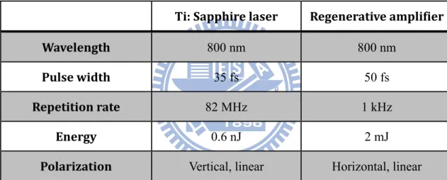
Table 4-1 Properties of Ti: Sapphire laser and regenerative amplifier ... 25
Table 5-1 Parameters comparison of Hall effect measurement and TDS fitting by Drude model ... 46
1
Chapter 1 Introduction
1.1 Terahertz Radiation
Generating short laser pulses has remarkably advanced recently. The availability of femtosecond laser pulses fosters a new field called terahertz optoelectronics.
Terahertz (THz) radiation, covering up the frequency gap between the infrared and microwaves, is generally about 100GHz to 30 THz. 1 THz is equivalent to 33.33 cm-1 in wave numbers, 4.1 meV photon energy, or 300 μm in wavelength, therefore THz waves are also known as sub-millimeter waves.
It was not until 1980s did people know about THz because the generation and detection technologies are not well-established. Since the appearance of ultrashort laser, THz has been rapidly studies. Mourou and Auston [1] in 1981 used the photoconductive switching to drive the antennas emitted terahertz in free space. In 1995, Wu and Zhang[2] applied the electro-optic effect of ZnTe crystal for free space terahertz sensing which increases the detection bandwidth and signal to noise
ratio(SNR).
Since the photon energy of terahertz wave are relatively smaller (4.1meV) than X-ray, so the applications of THz are diversified, such as THz imaging,
non-destructive measurement, studies on semiconductor nanostructures, medical sciences and security. More applications are still being researched in many areas by means of features of terahertz radiation.
2
Fig. 1.1-1 The spectrum range of electromagnetic waves (http://www.rpi.edu/terahertz/about_us.html)
For semiconductors, there are frequently characterized by three material parameters, the carrier concentration N, mobilityμand the scattering timeτ. Traditionally, mobility, carrier concentration and resistivity of semiconductor materials can be obtained via conventional four point probe and Hall effect
measurement by direct sample contact. Yet, conventional four point probe and Hall effect measurement can only obtain DC value of the sample. For some
semiconductors with high resistivity and low concentration, the electrical properties are difficult to be measured by simple direct contact because at the
metal-semiconductors interface, the Schottky barrier may disturb the measurement value. Hence, THz-TDS with advantages of non-contact and frequency-dependent measurement is a desirable for semiconductors characterization. THz-TDS is a coherent technology measuring both amplitude and phase information at the same time, which can avoid the uncertainty of Kramers-Kronig relation and simplify the analysis process. Besides, many researches have been performed on a variety of materials, such as dielectrics, semiconductors, liquids, superconductors, and nanostructured materials.
1.2 InN and InN:Mg Semiconductors
Indium nitride (InN) is a promising material for high frequency electronic devices. Compared to all other III-Nitride, InN has the lowest effective mass, the
3
highest mobility, the highest saturation velocity and the narrowest direct bandgap. Recently, indium nitride has received much attention since it extends the fundamental bandgap of III-Nitride compound semiconductors over a wide spectral region, ranging from near infrared to ultraviolet. It can be applied to high-frequency electronic
devices, near-infrared optoelectronics and high-efficiency solar cells. Moreover, the narrow bandgap (~0.7eV) and the rather large bandgap between the conduction minimum and the next local minimum of InN also make it a favorable candidate for terahertz emitters.
To achieve the InN-based devices, it is important to fabricate both n-type and p-type InN. However, due to its large electron affinity, InN is unintentionally doped n-type and difficult to be doped p-type. Nowadays, p-type doping of InN has been focus of intense efforts. To realize p-type InN, Mg is the most studied acceptor dopant in InN. Since it is the first time that Jones et al.[3] reported indirect evidence for p-type doping in InN. Besides,many groups have verified hole conduction[4] and p-type bulk Mg-doped InN films (InN:Mg) lies under a thin n-type inversion layer and a rather thicker depletion layer.[3-5] Nevertheless, whether Mg-doped InN films are p-type InN is still under debate because there is no direct evidence.
1.3 Organization of this Thesis
In chapter 1, an overview of THz radiation and brief introduction of InN and InN:Mg semiconductors. In chapter 2, the theoretical part of the THz generation and detection related to our experiments are illustrated. In chapter 3, semiconductor samples regarding to their basic properties, such as growth method and Hall measurement results will be introduced. In chapter 4, the experimental setups including the laser system and the free-space electro-optic THz-TDS system are characterized. The experimental results will be analyzed and discussed in chapter 5.
4
Finally, concluding remarks and future prospect are shownin chapter 6.
5
Chapter 2 Experimental Theories
2.1 Terahertz Radiation
THz pulses can be generated by many methods such as irradiation of photoconductive antennas, semiconductor surfaces, or quantum structures with femtosecond pulses. The most common mechanism are surge current and transient polarization which acts as broadband terahertz sources. In this work, the THz waves are generated via surge current.
Surge-Current Model
Basic mechanism of surge current begins with an ultrashort laser pulse which creates electron-hole pairs in semiconductors. Then the carriers accelerate in the external or internal electrical field to form a transient current which radiate THz waves.In the far field approximation, the radiated field is proportional to the time derivative of the photo-current.
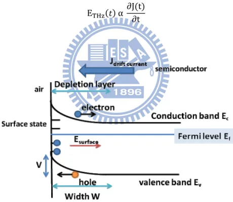
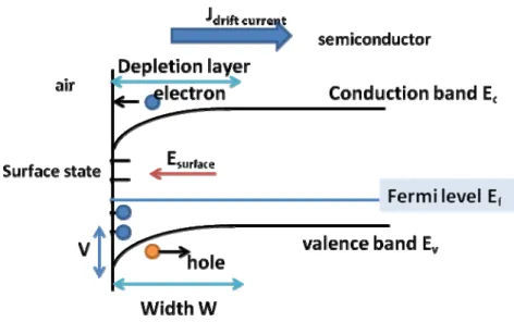
2.1.1 Surface Depletion Field
In semiconductors with wide bandgaps, such as GaAs (1.43 eV) and InP (1.34 eV), the surface states exist in the forbidden gaps within the bandgap and Fermi-level pinning occurs. The band bending leads to the formation of depletion region in which the surface built-in field exists. The depletion field is a function of Schottky [6] barrier potential and dopant concentration
E eN ε W W 2ε eN V kT e
6
Where N is dopant concentration, is permittivity, W is depletion width, V is the potential barrier and T is the thermal energy.
The field direction is normal to the surface. Generally, the energy band is bent upward for n-type semiconductor whereas downward for p-type.The built-in field in p-type semiconductor drives the electrons and holes leading to surge current after photon excitation. While in n-type semiconductors the electrons and holes are accelerated in opposite direction by the built-in field to drive a surge current. Thus the transient current radiates THz waves. The emitted THz radiation amplitude is proportional to the time derivative of the photo-current.
ETH α ∂J t ∂t
Fig. 2.1-1 Band diagram and the schematic flow of drift current in n-type semiconductor
7
Fig. 2.1-2 Band diagram and the schematic flow of drift current in p-type semiconductor
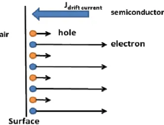
2.1.2 Photo-Dember Effect
In semiconductors with small bandgaps and small effective mass, such as InAs and InSb, radiate THz via Photo-Dember effect. With near IR light excitation (energy~1.55eV), the absorption depth is very small (~100nm)[7], and the excess energy of photoexcited carriers is very large in narrow-bandgap semiconductors. Thus these conditions enhance the Photo-Dember effect.
The band bending in narrow-bandgap semiconductors is not obvious resulting in a relative small surface depletion field. After the ultrafast laser excitation, the high absorption coefficient due to a small bandgap causes a large gradient carrier concentration. The excited electrons and holes diffuse in the same direction with different velocities, and therefore the Photo-Dember effect dominant. Because the electron mobility is always larger than the hole mobility, the direction of diffusion current is the same for both n- or p-type semiconductors. The fast photo-current rise and decay time due to the small electron mass and high mobility which often increase
8
with decreasing band gap is helpful for efficient THz generation. The need of photon energy is comparable small that makes the free carriers have large excess energy as well. The steady-state Photo-Dember voltage can be expressed by [8]:
VD KB T b T e 1 b 1ln 1 b 1 ∆n n b p
Where no and po are the intrinsic concentration of electrons and holes, μe and μn are
the mobility of electrons and holes, mobility ratio b µµ , and T
e and Th are the
temperature of photo-excited electrons and holes. Several properties can be derived from the equation: Photo-Dember effect is enhanced by larger electron mobility
), higher electron excess energy (αT
e) and low intrinsic carrier concentration.
The electric field E V (d is the absorption depth) is inversely proportional to absorption depth. Therefore, the Photo-Dember effect is stronger in narrow bandgap materials than in wide bandgap materials and is further enhanced by the small
absorption depth. InAs are very interesting semiconductor, especially as a strong THz emitter with high intensity. The high conversion efficiency has made InAs drawn much attention and be one of the most widely used THz emitters. InN has also been considered to generate THz waves via Photo-Dember effect[9]. In this project we will focus on the terahertz emission of InN and InN:Mg for different lattice structures.
9
Fig. 2.1-3 Schematic flow of diffusion current by photo-excited carriers near the surface of a semiconductor
2.2 Optical Rectification
If the applied optical field is considerably strong, it causes nonlinear optical phenomena. THz radiation field generated by the optical rectification, ETHz(t), is
proportional to the second-order nonlinear polarization in the near field. We can express the nonlinear polarization induced by optical rectification in the far field as
ETH t • ETH α •
∂ P t ∂t
Where e is the unit vector, which is normal to the observation direction at the observation point.
The strong dependence of the emitted THz radiation intensity on the crystal orientation to the pump polarization is the most unambiguous evidence for the contribution of the χ(2) process. By rotating a sample regarding to its surface normal, the relative contribution of the azimuthal angle-dependent component to the total THz radiation can be estimated.
2.3 Terahertz Detection
10
electro-optic sampling. These methods are coherent detection which can get both amplitude and phase information by scanning THz time-domain waveforms.
2.4 Electro-Optical Crystal and Free Space Electro-Optic Sampling (FS-EOS) The EO sampling method is based on a birefringence in a EO crystal induced by the incident radiation, or Pockels effect. Under the external field, the phase retardation induced in the EO crystal can be expressed as[ 10]
∆T 2π
λ dn γ ETH
Where d is the thickness of the crystal, n is the refractive index of the crystal at the wavelength of near IR probe beam, λis the probe beam wavelength, γ41 is the
electric-optic coefficient, and ETHz is the electric field of THz waves. Among all
crystals, ZnTe is commonly used for EO sampling of the THz pulse since it has relatively large electric-optic coefficient and is transparent at the wavelength of both Ti:Sapphire laser and THz radiation. The THz pulses are best detected by using free- space EO sampling method than photoconductive antennas due to the non-resonant method and is suitable for broadband detection.
The linearly polarized laser probe beam co-propagate with THz beam inside the crystal and its phase is modulated by the refractive index change induced by the electric field of the THz pulse. Suppose z is the probe beam and THz beam propagating direction, and x and y are the crystal axes of the EO crystal. When an electric field is applied to the EO crystal, the birefringence axes induced by electric field x’ and y’ are at an angle of with respect to x and y axes.If the input probe beam is polarized along x with amplitude Eo, then the output beam after rotating the
11 E E cosπ 4 sin π 4 sinπ 4 cos π 4 e 0 0 1 cosπ 4 sin π 4 sinπ 4 cos π 4 E 0 E 2 ee 11
Where δ=Γ0+Γ is the phase difference between the x’ and y’ polarizations,
including dynamic termΓcaused by THz field and static termΓ0.
The intensity of probe beam in x and y direction are I |E | I cos Γ Γ
2
I E I sin Γ Γ
2
Where Io=Eo2 is the input intensity. After the beams travel through the Wollaston
prism Ix and Iy can be extracted independently. The static term Γ0 is often set at
which provided by a quarter-wave plate for operating at the linear region to avoid distortion. We can measure the signal difference between Ix and Iy by a balance
detector.
I I I I Γ
Γ 2π
λ dn γ ETH
From above, we can obtain the whole time-domain waveforms by measuring the signal difference at the balance detector as a function of the THz pulse and laser probe pulse.
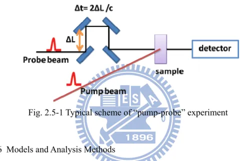
12 2.5 Pump Probe Technique
General principles of pump probe methods need two ultrashort pulses: one is called “pump” pulse which perturbs the sample at time t=0, and the other one is called “probe” pulse which crosses the perturbed sample and acts as probe. In order to investigate the transient dynamics, fine-scale analysis requires detection methods with response times which are as short as possible so we need an ultrashort laser to
overcome this problem.
Fig. 2.5-1 Typical scheme of “pump-probe” experiment
2.6 Models and Analysis Methods
A terahertz time-domain spectroscopy (THz-TDS) waveform transmitted through or reflected from materials provides frequency-dependent optical constants, due to its shape is modified by the material’s characteristic frequency response. The process of utilizing THz-TDS in determining the frequency-dependent optical constants of samples can be obtain by Fast Fourier Transform (FFT) of reference and sample signals without the need for Kramers-Kronig analysis. In general, the parameter extraction process of time-domain spectroscopy is stated as follow.
13
Fig. 2.6-1 The flow chart of THz-TDS measurement and the parameter extraction process
In the following section, we will explain the electromagnetic theories and analysis methods for thick samples and thin samples.
2.7 Thick Samples
For thick samples (typically >100μm), the temporal terahertz pulse performs clearly separated echoes which caused by multiple reflections in the sample. That is to say, the terahertz signal drops to nearly zero between two echoes. Thanks to the sample thickness, only the terahertz pulse transmitted directly through the sample is taken into account. Thus, we can cut the echoes to simplify the analysis, as shown in Fig. 2.7-1. The diagram of the electromagnetic model is shown as Fig. 2.7-2,
assuming plane wave and normal incidence. Now, let us consider Eo(ω), Eref(ω) and
Esample(ω) as the incident terahertz field, the reference field and the signal field
transmitted through the sample with thickness d, respectively. n 1 and
n n ik are refractive index of air and thick sample extracted from terahertz time-domain measurement.
14
E ω E ω t t e E ω t t e e
t and t are transmission coefficient from air (medium 1) to sample (medium 2) and from sample to air, which can be expressed as follow:
t 2n n n 2 1 n t 2n n n 2n 1 n
From Eq(2-16) and Eq(2-17), the complex transmission coefficient T ω of the sample is obtained by dividing the signal recorded with the sample E ω by recorded without the sample E ω
T ω E ω
E ω e e
4n 1 n
Complex transmission coefficient T ω of the sample as function of frequency can be derived from Fast Fourier Transform (FFT) of experimental time-domain signals E t and E t .
T ω E ω
E ω ρe ∆
Thus, complex refractive index can be obtained as
n 1 c∆φ ωd k c ωdln 4n ρ 1 n
15
Fig. 2.7-1 Terahertz time-domain waveform transmitted through thick silicon and both first and second echoes are well separated from the main signal
Fig. 2.7-2 Diagram of the electromagnetic model of thin sample
2.8 Thin Samples
In the case of thin samples, the overlap between successive echoes in
time-domain prevents us from dividing the terahertz signal transmitted through the sample into its successive echoes. Thus, when we extract the complex refractive index of the sample, we have to take the multiple reflections within the thin film into
16
account. Fig. 2.8-2 displays a schematic of the interaction of the THz pulse with the sample. Let Eo(ω), Eref(ω), Efilm(ω) and Esignal(ω) be the incident terahertz field, the reference field transmitted through substrate with thickness d’, the signal field transmitted through the thin film with thickness d and the signal field transmitted through both the thin film and the substrate, respectively. n 1, n n ik and n are refractive index for air, sample and substrate. Eref(ω), Esignal(ω) is expressed as
E ω E ω t t e ’ e E ω t t e e ’
E ω Ef ω t e ’
We suppose that it is a plane wave impinging on the front surface of the sample at normal incidence so that we do not have to consider the tilting angle in our
following calculation. Consider the multiple reflections within the thin film, Efilm(ω) is expressed as
Ef ω
E ω t t e E ω t t r r e E ω t t r r e
E ω t t r r e
Where q is the number of multiple reflections. tij and rij, reflection coefficient at
the i-j interface and transmission coefficient from medium i to medium j, referred to the Fresnel equations describe the transmission and reflection of the THz wave at each interface.
r n n
n n
t 2n
17
By assuming the number of multiple reflections are infinite, that is q→∞, the Efilm(ω) could be expressed as
Ef ω E ω
t t e 1 r r e
The theoretical complex transmittance can be given by
T ω, n E ω
E ω
t t e t 1 r r e
With complex refractive index of thin film n n k .
After collecting transmission time-domain THz signals by electro-optic sampling THz system. By virtue of fast Fourier transform (FFT), the time-domain signals are transformed into frequency domain. By dividing E ω and E ω , we have the theoretical complex transmittance. Apparently, there is no exact solution for the complex refractive index. For the sake of extracting complex refractive index, we use a numerical method and define error function as
T ω, n , k T ω, n , k Error function ω, n , k
If there exists a complex refractive index which makes the error function closest to zero at the certain frequency ω, we can extract the value at each frequency by using programs.
18
Fig. 2.8-1 Terahertz time-domain waveform transmitted through thin samples and the main signal is mixed with multiple reflection signals
Fig. 2.8-2 Diagram of the electromagnetic model of thin sample
2.9 Determination of Optical Conductivity and Mobility from Drude Model and Drude-Smith Model
19
dependent complex refractive index of thin films. The frequency dependent complex optical conductivity can be obtained from complex refractive index. First of all, we briefly introduce the theoretical part starting from Maxwell equations with simple conducting medium. The flowing current of the medium is J σE and the formula is
H J ∂D ∂t J ωε ε E ωε ε σ ωε ωε εE ε ε σ ωε
Where ε∞ is the contribution of the bound electrons and ε is the effective
dielectric constant. We can get ε by
ε ε ε n k
, and therefore the complex conductivity can be obtained from
σ ω σ σ ωε ε ε
σ ωε ε
σ ωε ε ε
It is well-known that Drude model explains the transport properties of electrons in materials, especially metals. This model considers that the microscopic behavior of electrons in a solid may be treated as freely moving particles subjected to random collisions under the influence of an applied field. According to classical simple Drude model[11], the conductivity can be expressed as follow
σ ω σ σ ε ω τ 1 ωτ σ ε ω τ 1 ω τ σ ωε ω τ 1 ω τ
20
The plasma frequency is defined as ω N , where N is carrier concentration, e is the electronic charge, m* is the effective carrier mass, and τ0 is carrier relaxation
time. The DC conductivity is given by σDC eNµ, where carrier mobility is µ .
The simple Drude model reveals that the collision process is random and the velocity of carriers is damped with time constant τ0. Many semiconductors in terahertz region
obey the simple Drude model, but still some materials, such as nanostructured materials cannot explain by simple Drude model. In recent times,Smith introduced a modified Drude model[12], which can explain the deviations from the simple Drude model, especially for the negative values of imaginary part. Smith proposed the complex conductivity in the Drude-Smith model by
σ ω ε ω τ 1 ωτ 1
c 1 ωτ
Where c is a parameter describing fraction of the original velocity of electron after scattering and varied from -1 and 1.In the Drude-Smith model, carriers retain a fraction c of their initial velocity. Mainly, c = 0 corresponds to the simple Drude conductivity and c = –1 means that carrier undergoes complete backscattering. The Drude-Smith model predicts a DC conductivity of σDC eNµ 1 c and thus the reduced macroscopic DC mobility is given by µ 1 c µ.
21
Chapter 3 Sample Properties
Indium nitride (InN) is a narrow bandgap semiconductor with bandgap energy around 0.7eV. It has received a great attention due to its small effective mass, high mobility and high saturation velocity which are very suitable for high frequency electronic devices. Moreover, the distance to next peak is 2.8eV preventing electrons from intervalley scattering. Fundamental properties of InN are listed below.
InN
Bandgap (eV) 0.7
Energy gap to next peak (eV) 2.8 Effective electron mass 0.07m0[13]
Mobility at 300k (cm2/Vs) 4000
Saturation speed (107 cm/s) 4.2
Table 3-1 Physical properties of InN[14]
In this thesis, a-plane and c-plane InN epitaxial films are studied. The crystal structure and atomic arrangement of a-plane and c-plane InN are shown in Fig.2.9-1 and Fig. 2.9-2. In the c-plane InN film, the stacking series of its wurtzite structure is ABABAB…along the -c-axis direction. In this growth direction, there are either In- or N-terminated polar surfaces in the surface layers. For a-plane InN, both In and N exist along the surface as shown in Fig 2.9-2. [15]
22
Fig.3-1 Crystal structure of InN[16]
Fig.3-2 Atomic arrangement of InN along the c- and a-plane 1010 and 1120 are crystal axis growth directions[15]
The a-plane InN epitaxial film (~1.2 μm) was grown by plasma-assisted molecular beam epitaxy (PA-MBE) on r-plane 1102 sapphire wafer, while the
c-plane 0001 InN epitaxial film (~1.2 μm) was grown on Si (111).
The a-plane InN:Mg films(~1.2 μm) were identical to a-plane InN grown on
r-plane 1102 sapphire wafer by plasma-assisted molecular beam epitaxy(PA-MBE)
while the c-plane 0001 InN:Mg films was grown on Si (111). The thickness is various as listed in Table 2. Mg doping was performed with a high-purity Mg(6N) Knudsen cell. The Mg doping level was controlled by regulating the cell temperature
23
between 180 and 270 °C. The electron concentrations and mobilities were determined by room-temperature Hall effect measurements.
Sample Thickness(μm) Mobility(cm2/Vs) Concentration(cm-3)
-c-plane 1.5 1036 3.1×10¹⁸
a-plane 1.2 298 7×10¹⁸
Table 3-2 List of Undoped InN samples
Sample Thickness(μm) Mobility(cm2/Vs) Concentration(cm-3)
-c-plane 080523 1.14 408.45 1.15×10¹⁸ -c-plane 080525 1.00 175.90 1.63×10¹⁸ -c-plane 080611 1.27 137.43 2.14×10¹⁸ -c-plane 080624 1.23 530.13 4.33×10¹⁷ -c-plane 090317 1.20 192.00 9.90×10¹⁷ a-plane 071125 1.20 62.04 4.09×10¹⁸
Table 3-3 List of Magnesium doped InN samples
0 200 250 5.0x10¹⁷ 1.0x10¹⁸ 1.5x10¹⁸ 2.0x10¹⁸ 2.5x10¹⁸ 3.0x10¹⁸ 3.5x10¹⁸ 4.0x10¹⁸ 4.5x10¹⁸ 5.0x10¹⁸ carrier concentration carrier concentra tion ( cm -3 ) Mg cell Temperature(oC)
24
Chapter 4 Experimental Setups
4.1 Femtosecond Laser System
In this work, we use an oscillator titanium sapphire laser and a titanium sapphire regenerative amplifier. The oscillator Ti: Sapphire laser is used as the seed laser which is guided to the Ti: Sapphire regenerative amplifier. Ti: Sapphire laser is pumped by a frequency-doubled diode-pumped Nd:YLF laser at 532nm with 5W power and provides 35fs pulses with wavelengths ranging from 750 nm to 850 nm. The pulse repetition rate is ~82MHz and the output power is up to 0.4 W. The seed laser is stretched to avoid damaging the amplifier crystal. The pump laser for the amplifier is Q-switched Nd:YLF laser at 527nm and output power 20W. The pulse width of the amplified beam is approximately 50fs with wavelength about 800nm. The repetition rate is 1 KHz and the output power is about 2W corresponding to 2mJ pulse energy.
25
Fig. 4.1-2 Schematic figure of pulse amplification
Ti: Sapphire laser Regenerative amplifier Wavelength 800 nm 800 nm
Pulse width 35 fs 50 fs Repetition rate 82 MHz 1 kHz
Energy 0.6 nJ 2 mJ Polarization Vertical, linear Horizontal, linear
Table 4-1 Properties of Ti: Sapphire laser and regenerative amplifier
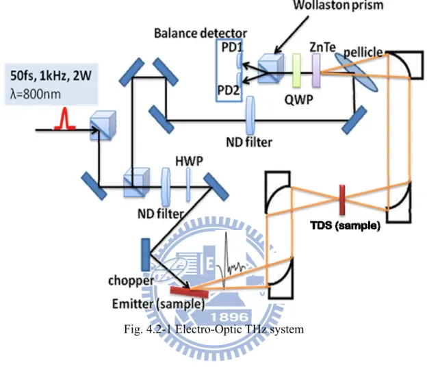
4.2 Experimental System (Electro-Optic THz System)
The setup of the Electro-Optic THz system is shown in Fig. 4.2-1. An amplified Ti: Sapphire laser providing 50fs, 800nm, 2mJ pulsed at repetition rate of 1kHz is used to drive this system. The linearly s-polarized incident beam is divided into two separated beams by a beam splitters. The reflected beam from the beam splitter is used as the probe beam to detect the THz signal and the transmitted beam from the beam splitter is used as the pump beam to excite the sample generating carriers which radiate THz pulse respectively. Polarization of the pump beam is rotated to p-
26
polarized by a half-wave plate (HWP). The p-polarized pump beam generates linearly p-polarized THz pulsed in a semiconductor surface emitter at the incident angle of 74.3° respect to the surface normal which is close to Brewster angle. All the reflected beam from the emitter is blocked by a Teflon sheet provided a high transmission to terahertz region. The generated THz radiation is collimated and focused onto the sample by a pair of gold-coated off-axis parabolic mirrors with focal lengths of 3 and 6 inches respectively. The transmitted THz radiation is again collimated and focused onto a 0.7-mm-thick (110) ZnTe crystal for free space electro-optic sampling by another pair of parabolic mirrors with the same focal lengths with previous pair.A pellicle beam splitter which is transparent to the THz beam and has a reflectivity of 5% for 800nm light is used to make the probe beam collinear with the THz beam in the 0.7mm-thick(110) ZnTe crystal. The linear polarization of the probe beam is perpendicular to the polarization of the THz beam and we adjust the azimuth angle of the ZnTe crystal to achieve the highest modulation efficiency. In order to increase the signal to noise ratio, an optical chopper and a lock-in amplifier are used.
Polarization of the probe beam modulated by the THz radiation is converted to ellipsoid polarization by a quarter-wave plate. Then the transmitted probe beam with polarization changed by EO effect is separated into a linear s-polarized beam and a p-polarized beam via a Wollaston beam splitter. These two orthogonal beams are coupled into balance detector with two photodiodes used to detect the differential signal between two individual probe beams and the signal is proportional to the THz electric field. A motor stage within the probe beam path is used to scan the delay time between the probe pulse and the THz pulse imposing on the ZnTe crystal to obtain the entire THz time-domain waveform. Balance detector is connected to a lock-in
amplifier to amplify the signal respect to noise, and then the signal can be obtained by a computer. The whole THz beam path is enclosed by an acrylic box which can be
27
purged with nitrogen gas to decrease the environmental humidity in order to avoid water vapor absorption.
28
Chapter 5 Experimental Result and Discussion
In this chapter, we first discuss the results of terahertz emission from c-InN,
c-InN:Mg, a-InN and a-InN:Mg samples. Afterward we discuss the terahertz
spectroscopic study of c-InN and c-InN:Mg samples.
5.1 Terahertz Emission of c-plane InN:Mg Epilayer
For research works related to terahertz, it is indispensible to develop a strong and efficient terahertz emitters. We investigated terahertz emission of several c-InN:Mg films with different carrier densities. To realize the effect of magnesium doping in the terahertz radiation of InN films, we measured the time-domain terahertz emission by free-space electro-optic sampling method. The pump laser fluence was around 200μJ /cm2. The terahertz waveforms of the several samples are shown in Fig. 5.1-1. We noticed that several samples exhibit negative terahertz polarity with concentration below 1×1018 cm-3, while those of samples with concentrations around 1.2×10¹⁸ , 1.6×10¹⁸ and 2.1×1018 cm-3 and the undoped InN (n=3.1×10¹⁸) have the positive polarity. The terahertz polarity of the InN:Mg samples is confirmed by comparing it to those of n-type and p-type GaAs wafers, which shows the opposite signs of polarity depending on the doping type. The observed negative polarity of InN:Mg samples with concentrations around 4.3×10¹⁷ , 9.9×1017 cm-3 are the same as that of the p-type GaAs.
29
Fig. 5.1-1 The time-domain THz waveforms of the undoped InN and Mg-doped InN films with different electron concentrations. THz waveforms of n- and p-type GaAs are also shown for comparison.
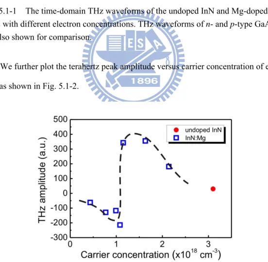
We further plot the terahertz peak amplitude versus carrier concentration of each film as shown in Fig. 5.1-2.
Fig. 5.1-2 The peak THz amplitudes of InN:Mg and undoped InN samples as a function of the electron concentration. Each sample was photoexcited at the pump
30
intensity at 200 μJ/cm2. The dashed line is drawn for eye-guiding.
From our previous study[17], we know the terahertz emission mechanism for small bandgap semiconductors is photo-Dember effect. However, in recent times, Lin
et al.[18] discovered the negative polarity of terahertz wave from an undoped n-type
InN excited at very low fluence below 590 nJ/cm2, indicating that the dominant radiation mechanism in InN is the drift current induced by the internal electric field. For highly excited InN, terahertz radiation induced by the surface electric field is overpowered and is dominated, conversely, by the photo-Dember field so that its polarity is positive.[19] The InN epilayers are grown on c-plane sapphire and Si(111) substrates by MOCVD. In Fig. 5.1-3, the polarity of the terahertz radiation field from InN is opposite to that from p-InAs whose radiation mechanism is dominated by the photo-Dember effect. As a result, terahertz emission from narrow bandgap InN is no longer dominated by photo-Dember effect but dominated by surface depletion field under low excited pump power.
31
p-GaAs, InN-A, and InN-B samples with 310 nJ/cm2 excitation density. [18]
Terahertz pulses can be generated either externally by separated electrodes in photoconductive antennas (PCA) or interally by the photo-Dember effect or by the surface depletion field close to the surfaces of semiconductors. In general, as we have mentioned in the previous chapter, the distinction between the photo-Dember effect and surface depletion field acceleration can be made by monitoring the polarity of terahertz wave. In wide bandgap semiconductors, such as GaAs (1.43 eV) and InP (1.34 eV), the surface states exist in the forbidden gaps within the bandgap and Fermi-level pinning occurs. Fermi level-pinning occurs to bend the bands and lead to the formation of surface built-in field in the depletion region at the surface. The direction of the bulit-in electric field induced by band bending for wide bandgap semiconductors depends on the dopant types. Fig. 5.1-1 shows that the directions of drift current and terahertz wave polarity are opposite for n-type and p-type GaAs.
The band bending in narrow bandgap semiconductors is not obvious due to the relative small surface depletion field. AndInN (0.7 eV) has the surface Fermi level located above the conduction band minimum and thus the surface band bending for both n-type and p-type InN is downward, as shown in Fig.5.1-4. Correspondingly, the terahertz wave polarities of n-type and p-type InN caused by surface depletion field are both negative.
32
Fig. 5.1-4 The band bending and carrier distribution of (a)n-type and (b)p-type a-InN are illustrated, where EF, EB, IL, n(z), and p(z)denote the bulk Fermi level,
surface branch point energy, electron inversion layer, free electron, and free hole spatial distributions. [5]
Nevertheless, in our work, we observed the several samples with negative terahertz polarity and terahertz emission caused by both the photo-Dember effect and surface depletion field is closely related to carrier concentrations. Both terahertz peak amplitude and polarity can be attributed the competition between these two
mechanisms at the certain concentration. The negative terahertz wave polarity is an exceptional result for c-InN. From previous research, the terahertz emission from
c-InN is dominated by the photo-Dember effect and therefore the terahertz polarity
must be positive regardless of dopant types. In addition, there is no azimuthal angle dependence of terahertz radiation for c-plane samples, the contribution of optical rectification effect is ruled out, as shown in Fig.5.1-5. Hence, the one and only possible explanation for negative terahertz wave polarity is the dominant surface depletion field effect due to the severe downward surface band bending from magnesium doped InN films.
33 0 50 100 150 200 250 300 350 -0.00010 -0.00009 -0.00008 -0.00007 -0.00006 -0.00005 -0.00004 -0.00003 -0.00002 -0.00001 0.00000 0.00001 c-InN:Mg 080624 Pe ak a m pl it ud e ( a .u .)
Azimuthal Angle (degree)
Fig. 5.1-5 Typical azimuthal angle-dependent terahertz radiation from InN:Mg film. (The negative sign of THz peak amplitude is due to the THz negative polarity of the sample.)
Besides, the concentration-dependent enhancement in terahertz radiation is observed from our InN:Mg samples. In Fig.5.1-2, we observe that the peak amplitude of terahertz radiation increases while the carrier concentration decreases from that of undoped InN film. The maximum positive terahertz wave polarity occurs for samples withn=1.2~1.5×1018 cm−3. In addition, for samples with lower carrier concentrations (<nc~1×1018 cm−3), the amplitude of terahertz radiation is converted to smaller
negative terahertz wave polarity. At the same time, we measured the optical pump fluence dependence of samples with both positive and negative polarity and observed that terahertz emission increases linearly with pump fluence as shown inFig. 5.1-6.
34
Fig. 5.1-6 The amplitude of terahertz emission field vs. pump fluence for InN:Mg films with n=4.3×10¹⁷ and 1.6×1018 cm−3. The sign of data of InN:Mg film with
n=4.3×1017 cm−3 is inverted to be positive.
The electron concentration decreases as the Mg doping level increases,
indicating that Mg dopants act as acceptors compensating those unintentionally doped n-type InN films. Consequently, Mg acceptors reduce the electron concentration in the InN:Mg films. In agreement to the surface depletion field model, the strongest terahertz emission and the largest depletion width ( 1
A D
n n
W ∝ − ) occur for a highly
compensated semiconductor with nA~nD.[19]
n |nA nD|
W 2 V kBT/e en
The band bending and charge distribution of p-type and n-type InN near the surface can be numerically simulated by solving Poisson equation[14], as shown in Fig. 5.1-7.
35
Fig. 5.1-7 Band bending (a and b) and charge distribution (c and d) near the surface of an n-type (a and c) and p-type (b and d) InN film. The bulk doping level in each case is labeled by Nd and Na, respectively.[14]
The negative terahertz polarity of InN:Mg samples with n<nc (1×1018 cm−3)
elucidates that the carriers in these samples are highly compensated and the large downward band bending extends to cover the penetration depth(d~133 nm)[20] of the pump pulse (800 nm). Even if the photo-Dember effect still exists in these samples, the terahertz emission is dominated by surface depletion field effect. In contrast, for those InN:Mg samples with n>nc(1×1018 cm−3), the band bending occurs across the
space-charge layer should be much shorter that the penetration depth (d) owing to the partial carrier compensation and the photo-Dember effect dominates terahertz
emission in the bulk region of InN:Mg.[19]In this bulk region, the reduction in screening of the photo-Dember field must be more significant as n decreases further from that of undoped InN. Hence, the enhanced positive polarity terahertz emission is
36
obtained before the sharp increase in depletion depth occurs near nc.
5.2 Terahertz Emission of a-plane InN:Mg Epilayer
Recently, our group has reported a-plane InN as an efficient THz emitter[16]. It was reported that the THz emission from a-InN is enhanced when compared to that of c-InN[16]. The THz emission power of a-plane InN is two orders of magnitude larger than that of c-plane InN. Moreover, the peak value of terahertz field of the a-plane InN film is comparable to that of n-type InAs, which is one of the strongest
semiconductor terahertz emitter reported in many literatures.
Fig. 5.2-1 Terahertz waveforms of a-plane and c-plane InN films [16]
The main reason is that, the structure of c-InN results in an electric field generated by In-N layers directly perpendicular to the surface. Therefore, the out-of-surface radiation would be significantly limited by the geometrical structure. There would be merely less than 1% of the radiated terahertz power from this dipole can escape the surface because of the small emission cone limited by the total reflection within a material of high refractive index. On the other hand, the layers of
37
the in-plane intrinsic electric field perpendicular to the a-axis, as shown in Fig. 5.2-2. Due to this in-plane electric field, the a-InN could create enhancement of terahertz radiation without external applied magnetic field.
Fig. 5.2-2 Ball-and-stick model of the a-plane InN surface
We concluded that the evidence of the enhancement of terahertz radiation from a-InN is primarily due to the acceleration of photo-excited carriers under the
polarization-induced in-plane electric field perpendicular to the a-axis, which effectively enhances the geometrical coupling of the radiation out of semiconductor. Furthermore, we are also interested in terahertz emission mechanism of Mg-doped
a-plane InN films.
We measured terahertz peak amplitude of a-InN:Mg films with different
concentrations and compared to that of the strongest c-InN:Mg film, as shown in Fig. 5.2-3. We observe that the terahertz emission of a-InN:Mg films are slightly stronger than the a-InN film in the low concentration region. And the most significant thing is, the terahertz peak amplitude of a-InN:Mg films is about the same order as the
strongest c-InN:Mg film even if the carrier densities of a-InN:Mg films are almost one order higher than those of c-InN:Mg.
38 2 4 6 8 10 12 0 20 40 60 80 100 c-InN:Mg c-InN a-InN a-InN:Mg THz Amplitude (a.u.) Carrier Concentration ( x1018 cm-3)
Fig. 5.2-3 Terahertz peak amplitude of a-InN and a-InN:Mg films compared with the strongest terahertz emission of c-InN:Mg film
There is one thing that has to be mentioned, c-InN:Mg films show strong concentration-dependence, whereas a-InN:Mg films show weak dependence on concentration. On the basis on our Hall effect measurement, the mobility of a-InN:Mg films are typically smaller than that of c-InN:Mg films. In consideration of
photo-Dember effect, the terahertz radiation peak amplitude is proportional to electron mobility and regardless of the crystal orientation. Consequently, terahertz radiation caused by photo-Dember effect is supposed to be much larger in c-InN:Mg than in a-InN:Mg. Yet, a-InN:Mg still shows the same order in terahertz peak amplitude as c-InN:Mg one. According to surface depletion model, the highest terahertz emission occurs when the native donors (nd) are highly compensated by
acceptors(na). For a-InN:Mg films, the concentrations are generally much higher than c-InN:Mg films so there should be only partially compensation of donors achieved by
39
terahertz emission is weaker. Meanwhile, it can also be supported by the positive polarity from all a-InN:Mg films.
For all the reasons we discussed above, the possible explanation for terahertz emission from a-InN:Mg is polarization-induced in-plane electric field along the surface which is the same mechanism as a-InN films. Because the terahertz radiation enhancement mechanism of a-InN and a-InN:Mg is associated with the orientation of electric field rather than photo-excited carriers or compensation of donors and
acceptors, terahertz emission do not depend on wide variation of carrier concentration by regulating the Mg cell temperature.
In addition, the azimuthal angle dependence measurement of a-InN:Mg and
a-InN is shown in Fig. 5.2-4. The result of doping Mg in a-InN is still the same as
undoped one. Therefore, doping Mg does not significantly affect on both terahertz emission mechanism and azimuthal dependence.
0 50 100 150 200 250 300 350 300 400 500 600 700 800 900 1000 1100 1200 a-InN:Mg a-InN T H Z pe ak a m pl it u de ( a. u. )
Azimuthal angle (degree)
Fig. 5.2-4 The azimuthal angle dependence of undoped a-InN and a-InN:Mg films 5.3 Terahertz Time-Domain Spectroscopy Measurement
40
can be studied from 0.3 to 2.1 THz. For parameters extraction, the temporal profiles of the terahertz pulses are recorded twice, the first time without the sample to be characterized, and the second time with the sample. The temporal profiles of the terahertz pulse measured with and without the sample are shown in Fig. 5.3-1.
All the InN samples were grown on (111) silicon substrates. Fig. 5.3-1 shows the time-domain THz waveforms transmitted through a silicon substrate (thickness~ 370 μm) and free space. The amplitude and phase spectrums of air and silicon are shown in Fig.5.3-2. The transmittance shown in Fig 5.3-3 is approximately 60% to 70%.
The extracted frequency-dependent refractive index and extinction coefficient are shown in Fig. 5.3-4 and Fig. 5.3-5. The refractive index value 3.4 is the same as our previous results. Besides, the extinction coefficient is less than 0.05 which could be ignored for later calculation.
0 3 6 9 12 15 -0.0004 -0.0003 -0.0002 -0.0001 0.0000 0.0001 0.0002 0.0003 0.0004 0.0005 0.0006 0.0007 Am pli tud e ( a. u .) Frequency (THz) Silicon Air
41
Fig. 5.3-2 The corresponding amplitude and phase spectrums of air and silicon
0.3 0.6 0.9 1.2 1.5 1.8 2.1 0.0 0.2 0.4 0.6 0.8 1.0 T ran sm it tan ce Frequency (THz)
42 0.3 0.6 0.9 1.2 1.5 1.8 2.1 3.0 3.2 3.4 3.6 3.8 4.0 Re fractive In d ex n Frequency (THz)
Fig. 5.3-4 Frequency dependent refractive index of silicon
0.3 0.6 0.9 1.2 1.5 1.8 2.1 -0.02 0.00 0.02 0.04 0.06 0.08 E xtin ction co effic ie n t k Frequency (THz)
Fig. 5.3-5 Frequency dependent extinction coefficient of silicon
After successful analysis of silicon substrate, we measured InN and InN:Mg films. The THz time-domain waveforms of the undoped InN epilayer and silicon substrate are shown in Fig. 5.3-6. The transmittance of sample is about 20%. The calculated complex refractive index and conductivity of the InN film are shown in Fig.
43 5.3-8 and Fig. 5.3-9, respectively.
0 5 10 15 20 25 -0.0003 -0.0002 -0.0001 0.0000 0.0001 0.0002 0.0003 0.0004 0.0005 E-fi el d (a. u .) Delay time (ps) Si InN
Fig. 5.3-6 The terahertz time-domain signal transmitted through silicon and InN film
0.0 0.3 0.6 0.9 1.2 1.5 1.8 2.1 2.4 0.000000 0.000002 0.000004 0.000006 0.000008 0.000010 0.000012 0.000014 Silicon InN Frequency (THz) Am plitude 50 100 150 200 0.0 0.3 0.6 0.9 1.2 1.5 1.8 2.1 2.4 Frequency (THz) Angle(de g)
44 0.3 0.6 0.9 1.2 1.5 1.8 2.1 0.0 0.2 0.4 0.6 0.8 1.0 Tra n sm itta nc e Frequency (THz)
Fig. 5.3-8 The amplitude transmittance of InN film
0.3 0.6 0.9 1.2 1.5 1.8 2.1 5 10 15 20 25 30 35 40 45 50 N k R efracti ve i n d e x Frequency (THz)
45 0.3 0.6 0.9 1.2 1.5 1.8 2.1 -100 -50 0 50 100 150 200 250 300 350 400 450 500 Real Imaginary Co ndu ct iv ity ( cm -1 O -1 ) Frequency (THz)
Fig. 5.3-10 Experimental data (open symbols) and fitting data (solid lines) complex conductivity of InN film
The real part conductivity of undoped indium nitride film decreases with increasing frequency, while the imaginary part slowly increases. This result can be fitted theoretically by using the simple Drude model. We use least square fitting method to fit experimental data. The best fitting curves are shown in Fig. 5.3-10. The fitting result agrees well with the experimental result. The fitting parameters
correspond to 41.72 THz, and τ 52.5 fs. Assuming m 0.075m for InN with carrier concentration about 2×1018 cm-3, these fitting parameters correspond to carrier density N 1.62×1018 cm-3, and the carrier mobility µ = 1231.17 cm2/V-s, in logical agreement with room-temperature electrical Hall effect measurement result of 2×1018 cm-3and 1231.17 cm2/V-s.
46
Concentration(cm-3) Mobility(cm-2/V-s)
Hall effect measurement 2.00×10¹⁸ 1120.00
TDS fitting 1.62×10¹⁸ 1231.17
Table 5-1 Parameters comparison of Hall effect measurement and TDS fitting by Drude model
Fig. 5.3-11 shows the terahertz time-domain waveform of silicon substrate and the c-InN:Mg film. The transmittance of c-InN:Mg films are apparently much large than that of the undoped InN film. Fig. 5.3-13 ,14 ,15, and 16 show the transmittance of each sample with different carrier concentrations from 4.3×10¹⁷ to 2.1×1018 cm-3. Doping magnesium acceptors into InN films enhances the transmittance of terahertz around three times.
0 5 10 15 20 25 -0.0003 -0.0002 -0.0001 0.0000 0.0001 0.0002 0.0003 0.0004 0.0005 E -fie ld (a .u .) Delay time (ps) Si InN:Mg
Fig. 5.3-11 The terahertz time-domain signal transmitted through silicon and InN:Mg film
47 0.0 0.5 1.0 1.5 2.0 2.5 3.0 0.000000 0.000002 0.000004 0.000006 0.000008 0.000010 0.000012 Frequency (THz) A m plitude 0 100 200 0.0 0.5 1.0 1.5 2.0 2.5 3.0 InN:Mg Frequency (THz) Ang le(deg) 0 100 200 0.0 0.5 1.0 1.5 2.0 2.5 3.0 Silicon Frequency (THz) Ang le(deg)
Fig. 5.3-12 The corresponding amplitude and phase spectrums of silicon and InN:Mg film 0.3 0.6 0.9 1.2 1.5 1.8 2.1 0.0 0.2 0.4 0.6 0.8 1.0 080624 Tra n sm itta nc e Frequency (THz)
48 0.3 0.6 0.9 1.2 1.5 1.8 2.1 0.0 0.2 0.4 0.6 0.8 1.0 080525 Transmi ttance Frequency (THz)
Fig. 5.3-14 The amplitude transmittance of InN:Mg 080525
0.3 0.6 0.9 1.2 1.5 1.8 2.1 0.0 0.2 0.4 0.6 0.8 1.0 090317 T ran sm it tan ce Frequency (THz)
49 0.3 0.6 0.9 1.2 1.5 1.8 2.1 0.0 0.2 0.4 0.6 0.8 1.0 080611 T ran sm it tan ce Frequency (THz)
Fig. 5.3-16 The amplitude transmittance of InN:Mg 080611
Fig. 5.3-18 to Fig. 5.3-25 show the refractive index and complex conductivity of each c-InN:Mg sample with different carrier concentrations. All of these samples cannot be well-fitted by either Drude model or Drude-Smith model since the carrier behavior no longer obey the free electron model.
When it comes to doped semiconductors, it is useful to make a clear
distinction between heavy and light doping. In our case, the Mg doped InN films are lightly doping because of the existence of both positive and negative terahertz polarity. From our experimental data, the imaginary part of conductivity with a negative value keeps decreasing as the frequency increases. As the explanation of Drude-Smith model, the negative imaginary part of conductivity is attributed to the backscattering of electrons at interface and surface or grain boundary. Unlike Drude-Smith model, the free electrons are confined by the morphology of nanostructure, Mg doped films are mainly due to the hopping carrier transport. To interpret our data, the carrier transport may be dominated by electron hopping through these deep compensation centers. After the InN:Mg films were compensated, the Mg acceptor states could be
50
viewed as deep compensating defects. The transport is dominated by electron hopping through deep compensation centers or through diffusion since there exists a small but finite overlap of localized electron wave functions of defect centers.[21]Therefore, the negative imaginary part of conductivity can be tentatively due to the defects so the carriers are no longer behaved as free carriers.
51
Fig. 5.3-188 Experimental data of (a) refractive index and extinction coefficient (b) complex conductivity of InN:Mg film 080624
0.5 1.0 1.5 2.0 0 5 10 15 20 N k Ref ract ive i n d ex Frequency (THz)
52 0.3 0.6 0.9 1.2 1.5 -5 0 5 10 15 20 N k R efracti ve i n d e x Frequency (THz)
Fig. 5.3-19 Experimental data of (a) refractive index and extinction coefficient (b) complex conductivity of InN:Mg film 080525
53 0.3 0.6 0.9 1.2 1.5 1.8 2.1 -5 0 5 10 15 20 N k R efracti ve i n d e x Frequency (THz)
Fig. 5.3-20Experimental data of (a) refractive index and extinction coefficient (b) complex conductivity of InN:Mg film 090317
54 0.3 0.6 0.9 1.2 1.5 -5 0 5 10 15 20 N k R efracti ve i n d e x Frequency (THz)
Fig. 5.3-21 Experimental data of (a) refractive index and extinction coefficient (b) complex conductivity of InN:Mg film 080611
55
Chapter 6 Conclusion and Future Work
6.1 Conclusion
In this work, we investigated the emission mechanisms of both c-plane and
a-plane InN:Mg and terahertz time-domain spectroscopy of c-InN:Mg.
For THz emission study of c-plane InN:Mg, we corroborate by doping
magnesium as acceptors in InN films and found that there is a transition of dominant terahertz emission mechanism between the photo-Dember effect and surface depletion field depending on the carrier concentration. The polarity of THz waves can be
determined by the competition between these emission mechanisms at near the critical concentration nc~1.0×1018 cm-3. With the carrier concentration below nc, the dominant
terahertz emission mechanism is surface depletion field so that the terahertz polarity is negative. The significant intensified terahertz wave with positive polarity may be due to the enhanced photo-Dember field with reduced screening in those partially
compensated samples.
For THz emission study of a-plane InN:Mg, we indentified that the intensity of terahertz radiation from a-plane InN:Mg is at least two orders stronger than that of
c-plane InN film with a similar carrier density. The terahertz emission of both a-InN
and a-InN:Mg are polarization-induced in-plane electric field which is, unlike
c-InN:Mg, nearly independent of carrier density.
For terahertz time-domain spectroscopy of c-InN:Mg, we successfully
demonstrated that optical properties of undoped InN film can be described by Drude model. In addition, we tentatively explain the large negative imaginary part of conductivity of c-InN:Mg films is due to the hopping carrier transport.
6.2 Future Work
56
fabricate InN-based p-n junctions. However, if InN:Mg is p-InN is still under debate. It is important to develop a direct method to identify the doping type of InN. Terahertz emission measurement only tells the dominate mechanism of Mg:InN, yet still cannot directly proof whether InN:Mg is p-type. Currently, we are trying to find the possible solution of distinguishing p-type and n-type InN.
Monte Carlo dynamics model, finite-difference time-domain (FDTD) simulation technique for doped materials can be further developed to confirm our experimental data. To realize the transient carrier dynamics of Mg doped InN films, it is also important to investigate the InN:Mg films by optical pump-terahertz probe system.