© 2002 The Electrochemical Society. 关DOI: 10.1149/1.1524613兴 All rights reserved.
Manuscript submitted February 3, 2002; revised manuscript received July 2, 2002. Available electronicallyNovember 21, 2002.
Layers of polycrystalline silicon 共polysilicon兲 are used exten-sively in the fabrication of silicon metal-oxide semiconductor
共MOS兲 devices. Generally, these films are heavily doped to
mini-mize their electrical resistance, and are used to form gate electrodes and interconnections in MOS integrated circuits or charge-coupled devices. They are also used as emitter contacts in bipolar transistors and resistors.1-4The ongoing trend to scale down devices demands a reduction in the thickness of polysilicon films and inter poly oxides, to yield a higher integration density. Moreover, innovative device structures such as vertical thin film transistors共VTFTs兲5,6and pro-cesses have been proposed to increase chip packing density. They are suited to high density integration since their channel lengths are determined by the thickness of SiO2or polysilicon films, rather than by the photolithographic limitations. However, to our knowledge, no research has discussed the quality of the vertical polyoxides grown on the sidewall of a polysilicon thin film, on which the vertical device is to be made. Therefore, the quality of the vertical polyoxide for the nonplanar structure device, including the dielectric break-down field (Ebd) and the charge to breakdown (Qbd) must be studied.7,8
Over the last year, we have researched the quality of thermally grown oxides on the vertical sidewalls of polysilicon films and the results have been submitted to IEEE Electron Device Letters. In this work, however, we consider these oxides in more detail. Addition-ally, a low temperature plasma enhanced chemical vapor deposition
共PECVD兲 oxide is fabricated on the sidewall for further research.
The experimental results indicate that the vertical polyoxide can yield an Ebdand Qbdcomparable to those of the conventional planar oxide grown on single crystal silicon. This improvement comes pri-marily from the reduced number of grain boundaries on the vertical wall of the polysilicon film.
Experimental
Figure 1 shows the vertical structure used in the experiments. A 500 nm silicon dioxide film grown on a p-type silicon共100兲 wafer was used as an isolation layer by wet thermal oxidation. Then a 1
m thick polycrystalline silicon film 共poly-I兲 was deposited by low
pressure CVD 共LPCVD兲 on the oxidized wafer and doped with POCl3to yield a substrate polysilicon layer with 10-20⍀/䊐 sheet resistance. The deposition process was separated into one to six steps to yield a polysilicon film with various numbers of layers, but with the same total thickness to investigate the effect of grain boundaries in the vertical sidewall of the polysilicon film. Then, a 300-500 nm PE-tetraethylorthosilicate 共PE-TEOS兲 polyoxide film was deposited by PECVD on poly-I to isolate the gate and the sub-strate in the planar region. Thereafter, the top isolation oxide and poly-I were patterned to form the vertical sidewall by dry etching.
Before inter poly oxides were formed, a thin sacrificial oxide film was grown by wet thermal oxidation and then stripped for par-tial samples to perform a sacrificial process. After standard RCA cleaning, gate oxides with three different thicknesses were grown using a thermal furnace or deposited by PECVD. The temperature of the furnace was 900°C, in a dry O2ambient, and the PECVD was performed at 300°C with TEOS vapor. For PECVD TEOS deposi-tion samples, an addideposi-tional 900°C rapid thermal anneal共RTA兲 an-nealing in N2O ambient was applied to improve the quality of the oxide. The polysilicon gate was then formed and capped with a layer of passivation oxide. Finally, Al contact patterns were formed and used to create ohmic contacts.
The top views of devices include two patterns, one circular and the other square, as shown in Fig. 2a, designed to investigate the influence of corners on the quality of the vertical polyoxide. The border length of square patterns is 200m, and the radius of circu-lar patterns is 150m. Figure 2b depicts the scanning electron mi-croscopy共SEM兲 image of the sidewall of the square pattern after dry etching. The step in this figure included 1m of polysilicon sub-strate and 300 nm of isolation oxide.
The sheet resistance was measured using a four-points probe and the thickness was determined by cyclic voltammetry共CV兲 measure-ment. Finally, an HP 4156B was used to measure the current-density potential共J-E兲, Ebd, and Qbdcharacteristics. Capacitors with an area of 1.6⫻ 10⫺5 cm2were used to measure the capacitance.
Results and Discussion
The results of CV measurement cannot be considered alone to determine the thickness of the vertical polyoxides on the sidewall of polysilicon films, because of the parasitic capacitance. Figure 3 pre-sents the capacitance distribution in the vertical structure. The pure capacitance induced by the vertical oxide is labeled as C3k, C4k, or C5k as shown in Fig. 3. The thickness of the isolation oxide was changed from 300 to 500 nm to determine the parasitic capacitance induced by the bottom polysilicon and the extension of the vertical gate in the isolation oxide region. The capacitors effectively created between the bottom polysilicon and the gate in the vertical region are C3k, C4k, and C5k as shown in Fig. 3. The bottom polysilicon and top overlap gate also generate an additional parasitic capaci-tance. Two overlapping lengths, 5 and 10m are designed to realize this capacitance. The generated capacitors are labeled as C5u and C10u as shown in Fig. 3. The total capacitances, obtained with iso-lation oxides of different thicknesses, obtained by CV measurement, are labeled Cm3k, Cm4k, or Cm5k. Hence these capacitors are re-lated by
C3k, 4k, or 5k⫽ Cm3k, 4k, or 5k ⫺ C5u or 10u 关1兴 This equation yields C3k, C4k, and C5k for different gate oxide thicknesses. Finally, C3k, C4k, and C5k can be plotted and the ca-zE-mail: [email protected]
pacitance for zero isolation oxide thickness can be extracted as Cini. Then the oxide thickness in the vertical direction is given by
Tox⫽ kA/Cini 关2兴
where A has capacitor area 1.6⫻ 10⫺5 cm2.
Figure 4 shows the fitting plot of the capacitance of the 10.6 nm vertical polyoxide. The vertical capacitance increases from 13.41 to 14.49 pF as the thickness of the isolation oxide increases from 300 to 500 nm. The pure vertical capacitance is extracted as 11.22 pF, and the vertical polyoxide thickness is 10.6 nm. Transmission elec-tron microscopy共TEM兲 is used to verify the fitted results. Figure 5 shows TEM images of oxides on共a兲 vertical sidewall and 共b兲 planar polysilicon film. The thickness of the vertical polyoxide is about 10
Figure 1. Cross section of vertical polyoxide structure.
Figure 2. 共a兲 Designed patterns of vertical polyoxide structure. 共b兲 SEM
image of the sidewall of the square pattern after dry etching.
Figure 3. Parasitic capacitance distribution in vertical polyoxide structure.
Figure 4. Oxide thickness-fitting curve for thermal vertical polysilicon
nm, and the thickness of the planar polyoxide is about 20 nm, ac-cording to the TEM results. This result is of the same order as the fitted data, 10.6 and 18.5 nm.
Table I lists the final oxide thicknesses. The oxide thicknesses of planar structures are measured from planar polysilicon oxides, under the same substrate and oxide conditions as for vertical polysilicon oxides. This table reveals that the growth or deposition of oxides is much slower in the vertical direction than in the planar direction, because the grain boundary density and the gas adsorption rate are lower on the sidewall of the polysilicon layers.9
Figure 6 shows Ebddistributions of the thermal vertical polyox-ides for three different thicknesses, where 6.5, 10.6, and 18.2 nm are the thicknesses of the oxide grown on the vertical sidewall of poly-silicon films. For each thickness, data for samples with and without presacrificial oxidation are presented. A thinner vertical polyoxide yields a larger Ebd.10,11The presacrificial oxidation samples exhibit lower Ebds, especially⫹Ebds. This result is believed to follow from the increase in the roughness of the surface due to presacrificial oxidation. However, the Ebdvalues of circular samples are approxi-mately the same as those of the square samples; that is, the corner
effect is insignificant for the thermal vertical polyoxide, because the sharp corners have been smoothed during high temperature oxida-tion, and thereafter do not affect the quality of vertical oxide.
Figure 7 shows Ebd distributions of the 10.7-13.9 nm thick PECVD TEOS vertical polyoxides. As the vertical oxide thickness
Figure 5. TEM images of oxides on 共a兲 vertical sidewall and 共b兲 planar
polysilicon film.
Figure 6. Ebddistributions of vertical thermal polyoxides with three thick-nesses, 6.5, 10.6, and 18.2 nm. S and C represent square and circular pattern samples.共⫹兲 and 共⫺兲 indicate the positive and negative gate bias applied to gate.
Figure 7. Ebddistributions of vertical PECVD polyoxides with three thick-nesses 6.5, 10.6, and 18.2 nm. S and C represent square and circular pattern samples.
Table I. Oxide thickness of planar and vertical polysilicon oxides.
Gate oxide condition Planar structure thickness 共Å兲 Vertical structure thickness 共Å兲 Thermal 100 100 65 Thermal 200 185 106 Thermal 300 284 182 PECVD 100 138 107 PECVD 200 184 118 PECVD 300 311 139
increases, the Ebdremains almost constant or increases slightly. This trend is the same as for low temperature deposited oxide, prepared on conventional planar structures. The samples with presacrificial oxidation exhibit a higher Ebdthan do samples without the oxida-tion. The result follows from the fact that the reactive ion etch共RIE兲 process used to form the substrate patterns damages the polysilicon sidewall. However, the PECVD deposition temperature is too low to anneal the residual damage. Hence, an additional presacrificial oxi-dation process is required to remedy these defects, unlike for the thermal vertical oxide. The corners clearly degrade the vertical ox-ides’ Ebdvalues. In particular, for samples without presacrificial oxi-dation, the Ebd values of the samples with circular patterns are higher than those of the samples with square patterns.
Figure 8 presents Qbd values of the same samples as were considered in Fig. 6. These samples are stressed at⫹50 mA/cm2 for⫹Qbdand⫺5 mA/cm2for⫺Qbd. The Qbdvalues are approxi-mately two orders higher than those of the conventional planar poly-oxides. Also, a thinner polyoxide corresponds to a higher Qbd. For the 6.5 nm sample, Qbdcan be as high as 10 C/cm2, because poly-silicon grains in the vertical direction are columnar, so the grain boundaries are fewer than in the horizontal direction. Additionally, the samples with presacrificial oxidation have higher Qbd values. Although the additional oxidation increases the roughness of the substrate, the surface damage induced by RIE or remnant impurities on the bottom polysilicon surface can be removed by sacrificial oxidation, reducing the number of traps in the bulk of the polyoxide, thereby decreasing Ebdbut increasing Qbd.
Figure 9 shows Qbdfor the PECVD vertical polysilicon oxides. These samples are stressed at⫹0.1 mA/cm2to yield⫹Qbdand⫺5 mA/cm2 to yield ⫺Qbd. Qbd increases with the thickness of the PECVD oxide because of the instability at the beginning of PECVD oxide deposition. The Qbdvalues of these vertical samples also ex-ceed those of conventional planar PECVD TEOS polyoxides. Be-sides, samples with the preoxidation process also have higher Qbd values than samples without the preoxidation process. We believe that the major cause of the increase in Qbdis the reduction of RIE-induced damage in the polysilicon sidewall. However, the Qbd val-ues of circular samples are approximately the same as those of
square samples, and the corner effect is insignificant for the vertical polyoxide.
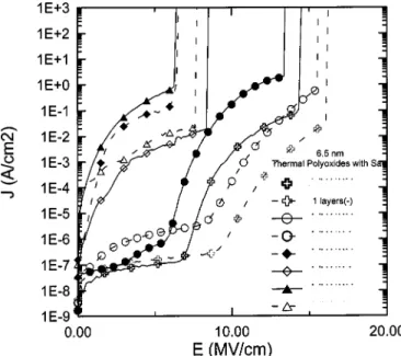
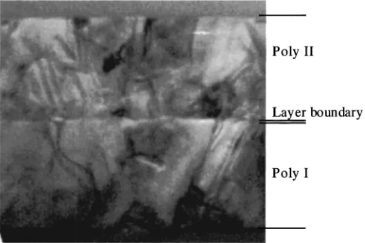
Figures 8 and 9 show that the vertical polysilicon oxides have much higher Qbd values than do conventional planar polysilicon oxides. This result follows from the lower grain boundary density in the vertical direction of the polysilicon. This suggestion was checked by changing the substrate’s structure and measuring the results, as plotted in Fig. 10. Figure 10 presents J-E curves of ver-tical oxides with the same thickness, 6.5 nm, but were made on the sidewall of several equally thick polysilicon substrates with various numbers of layers. Figure 11 presents a TEM image of a two-layered
Figure 8. Qbddistributions of the three vertical thermal polyoxides in Fig. 5. Figure 9. Qbd distributions of the three vertical PECVD polyoxides in Fig. 6.
Figure 10. J-E curves of vertical oxides with the same thickness of 6.5 nm,
but made on the sidewall of several equally thick polysilicon substrates with various numbers of layers.
polysilicon film. This figure shows that the grains grow from the bottom to the top, to form a single grain in the vertical direction. Hence, the number of polysilicon layers controls the numbers of vertical grains in polysilicon. The J-E curve degrades away from the standard Fowler-Nordheim 共F-N兲 characteristics as the number of layers increases. This experiment demonstrates clearly that the in-crease in the number of polysilicon layers inin-creases the number of grain boundaries in the vertical direction, degrading the quality of the grown polyoxide. The improvements in the vertical polyoxide result from the reduced number of grain boundaries in the vertical direction of the deposited polysilicon substrate.
This work was partially supported by the National Science Coun-cil of the Republic of China under contract no. NSC89-2218-E009-069.
National Chiao Tung University assisted in meeting the publication costs of this article.
References
1. C. H. Kao, C. S. Lai, and C. L. Lee, IEEE Electron Device Lett., 44, 526共1997兲. 2. L. Faraone, IEEE Trans. Electron Devices, ED-33, 1785共1986兲.
3. S. L. Wu, T. Y. Lin, C. L. Lee, and T. F. Lei, IEEE Electron Device Lett., 14, 113 共1994兲.
4. E. G. Lee and J. J. Kim, Thin Solid Films, 226, 123共1993兲.
5. C. S. Lai, T. F. Lei, and C. L. Lee, IEEE Electron Device Lett., 17, 199共1996兲. 6. T. Zhao, M. Cao, K. C. Saraswat, and J. D. Plummer, IEEE Electron Device Lett.,
15, 415共1994兲.
7. H. J. Mattausch, H. Baumgartner, R. Allinger, M. Kerber, and H. Braun, IEEE Trans. Electron Devices, 47, 1251共2000兲.
8. H. J. Mattausch, R. Allinger, M. Kerber, and H. Braun, IEEE Electron Device Lett., 19, 402共1998兲.
9. S. Wolf and R. N. Tauber, Silicon Processing for the VLSI ERA, Chap. 7, Lattice Press, Sunset Beach, CA共1986兲.
10. C. M. Osburn and D. W. Ormond, J. Electrochem. Soc., 119, 591共1972兲. 11. E. Harari, J. Appl. Phys., 49, 2478共1978兲.