properties
T. S. Ko, C. P. Chu, J. R. Chen, Y. A. Chang, T. C. Lu, H. C. Kuo, and S. C. Wang
Citation: Journal of Vacuum Science & Technology A 25, 1038 (2007); doi: 10.1116/1.2710244 View online: http://dx.doi.org/10.1116/1.2710244
View Table of Contents: http://scitation.aip.org/content/avs/journal/jvsta/25/4?ver=pdfcov Published by the AVS: Science & Technology of Materials, Interfaces, and Processing
Articles you may be interested in
Electroluminescence of Sn O 2 p - Si heterojunction Appl. Phys. Lett. 92, 121908 (2008); 10.1063/1.2902299
Local bonding analysis of the valence and conduction band features of TiO 2 J. Appl. Phys. 102, 033707 (2007); 10.1063/1.2764004
Defect energy levels in HfO 2 high-dielectric-constant gate oxide Appl. Phys. Lett. 87, 183505 (2005); 10.1063/1.2119425
Deep-level optical spectroscopy investigation of N-doped TiO 2 films Appl. Phys. Lett. 86, 132104 (2005); 10.1063/1.1896450
Observation of bulk HfO 2 defects by spectroscopic ellipsometry J. Vac. Sci. Technol. A 22, 1337 (2004); 10.1116/1.1705593
2 3
on their optical properties
T. S. Ko, C. P. Chu, J. R. Chen, Y. A. Chang, T. C. Lu,a兲 H. C. Kuo, and S. C. Wang Department of Photonics and Institute of Electro-Optical Engineering, National Chiao Tung University, 1001 Ta Hsueh Rd., Hsinchu 30050, Taiwan, Republic of China
共Received 26 September 2006; accepted 24 January 2007; published 2 July 2007兲
The authors reported the synthesis of indium oxide nanocrystal chains on silicon substrates using gold nanoparticles as catalyst on native silicon dioxide. Scanning electron microscopy investigations showed that In2O3nanocrystal chains were formed. The nanocrystal chains comprised many well shaped octahedron nanoparticles with their size ranging from 20 to 100 nm connected with each other to form a network. Both high resolution transmission electron microscopy and diffraction pattern revealed that the In2O3 nanocrystal chains were single crystalline grown along the 关111兴
direction. Photoluminescence study of In2O3 nanocrystal chains exhibited main photoemission at
544 nm due to the recombination between electrons in localized state induced by oxygen vacancies and holes in valence band. After the annealing treatment, the main photoluminescence peak not only slightly redshifted to 558 nm but also became narrower, which was attributed to the total localized state away from the conduction band caused by less defect distribution. © 2007 American Vacuum
Society. 关DOI: 10.1116/1.2710244兴
I. INTRODUCTION
Indium oxide共In2O3兲 is a very important wide band gap
of around 3.5 eV semiconductors and has recently attracted much interest as a material for transparent electrodes in elec-tronic devices such as liquid crystal displays,1 solar cells,2 sensing material,3and nanowire technology.4In recent years, there has been increasing interest in the fabrication of In2O3 nanostructure because of their advantages to the understand-ing of novel physical properties and potential applications in nanoelectronic and optoelectronic devices. Kong and Wang obtained In2O3nanobelts by evaporation of In2O3powders.5
Li et al. grew In2O3 nanowires by a thermal evaporation
oxidation method with a catalyst by laser ablation.6 Alina Magdas et al. grew In2O3 nanoarrows in thermally treated
indium nitride for different times.7 Lao et al. observed nanochains and nanowire networks grown by a vapor trans-port and condensation method.8Though many kinds of nano-structure of In2O3 were developed, the reports related to
nanochain structure of In2O3 are still limited substantially. In this article, we successfully synthesized In2O3
nanochains on silicon substrates using gold nanoparticles as catalyst on native silicon dioxide. The growth mechanism will be discussed in the following section. The structural and optical properties of In2O3 nanochains were analyzed in
de-tail by scanning electron microscopy共SEM兲, high resolution transmission electron microscopy 共HRTEM兲, x-ray diffrac-tion 共XRD兲, and photoluminescence 共PL兲. The method of thermal annealing was also used. We investigated the effect of thermal annealing on optical properties of In2O3
nanochains and described the reasonable mechanism in pho-ton emission.
II. EXPERIMENTS
Single crystal 共001兲 oriented silicon wafers were used as substrates. Gold nanoparticles having diameters of ⬃20 nm were used as catalysts; they were produced by the chemical reduction of gold chloride tetrahydrate 共HAuCl4兲 with
so-dium citrate, and then spread onto a silicon wafer coated with a native oxide layer using a self-assembled monolayer of 3-aminopropyltrimethoxysilane as an adhesion agent. A two-zone vacuum furnace was used to grow the nanochains. Oxygen was the carry gas and flowed through the system at rate of 30 SCCM 共SCCM denotes cubic centimeter per minute at STP兲. During the growth process, 2 g indium pow-ders were positioned at the upstream with the samples placed at the downstream. The source vapor was transported by the carrier gas and condensed on the substrates. The tempera-tures were heated to 900 ° C for sources and 700 ° C for samples. The typical reaction time was 6 h and the growth pressure was around 0.1 torr. The morphology and micro-structure of the samples were investigated by scanning elec-tron microscopy 共JEOL, JSM 6500F兲 and high resolution transmission electron microscopy共JEOL, JEM 2010F, oper-ating at 200 kV兲. The compositions were analyzed using en-ergy dispersive spectrometry 共EDS兲 attached to the SEM. Selected area electronic diffraction confirmed crystal orien-tation of In2O3nanochains. Afterward, the samples were
fur-nace annealed in the temperature of 700 ° C for 2 h in oxy-gen ambient. The crystal structure analysis was performed by the XRD measurement with Cu K␣ radiation. PL spectra were measured at room temperature by means of TRIAX-320 spectrometer using a 25 mW He–Cd laser with the emis-sion wavelength of 325 nm as the excitation source.
III. RESULTS AND DISCUSSION
In general, for one-dimensional nanostructure growth, many researches have shown that the synthesis using vapor-a兲Electronic mail: [email protected]
liquid-solid mechanism could obtain a constant diameter or periodically changing diameter along the growth direction without the presence of many nanocrystals with different sizes.9–11 In contrast, we obtained very interesting self-assembled In2O3nanocrystal chains with many nanoparticles
of different sizes when growth pressure was 0.1 torr and temperature was 700 ° C. Figures 1共a兲 and 1共b兲 show these self-assembled In2O3 nanochains and networks. The
nanochains have diameters of between 20 and 100 nm and length of around a few micrometers. They were connected with each other to form a complicated nanonetworks. A large number of the nanoparticles of the chains would aggregate near the network junctions. Yang and Lieber grew MgO nanochains and suggested that such morphology of nanochains was grown by a vapor-solid共VS兲 mechanism.12 Based on our experiment results, we found that the gold catalyst is necessary for the synthesis of the networks. How-ever, we also observed many gold nanoparticles distributed on the substrate surface, which means the indium vapor from the upstream formed alloy with several gold nanoparticles. Meanwhile, there were also many aggregative octahedral In2O3nanoparticles randomly dispersed on the substrate sur-face. In our growth process, therefore, the VS mechanism and gold catalyst played very important roles. We suggested it was likely that small octahedral In2O3 nanoparticles were
formed in air and fell on the substrate at first. Consequently, the gold catalysts nucleated with the adjacent In2O3
nanopar-ticles to start nanochain growth. Once the latter indium vapor reacted with leakage oxygen near the original In2O3
nanoparticles/nanochains, there were more opportunities to form sequence of In2O3 nanoparticles and then synthesized
long nanochains. We focused on different positions of In2O3
nanochains to proceed EDS measurement. The EDS
spec-trum, shown in the Fig. 1共c兲, indicates that the nanochains were essentially composed of indium and oxygen. The sili-con peak came from silisili-con substrate and no gold was de-tected so that we suggested the gold may still remain on the substrate. Lao et al. grew In2O3nanocrystal chains of similar
shape as ours by using gold catalyst; meanwhile, they also found that there was not any gold within their nanochain structure.8
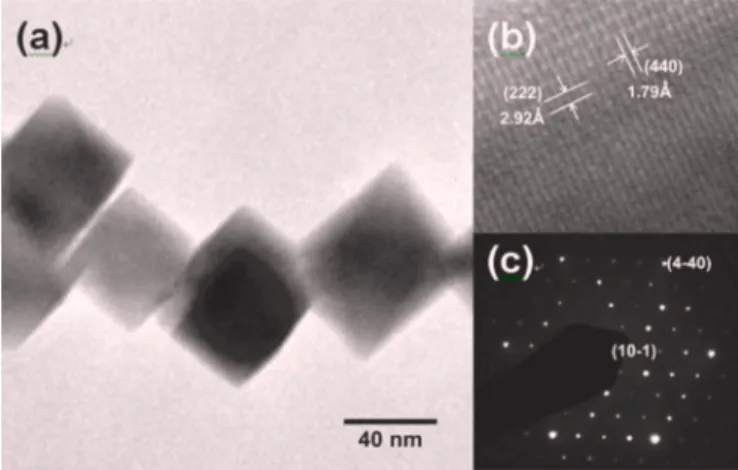
Figure 2共a兲 shows the selected TEM bright-field image of In2O3nanochains. The sizes of every particle in chains were
different but the shapes were uniquely octahedral shape. The junction boundary can be clearly seen between the two nano-particles. Figure 2共b兲 shows the high resolution TEM image of one nanoparticle. The corresponding selected area electron diffraction共SAED兲 is shown in Fig. 2共c兲, which proved our In2O3nanoparticle with chains was a single crystal structure
of excellent quality. Analysis of both TEM images and SAED revealed that the In2O3nanochains are single
crystal-line and grow along the关111兴 direction.
We would further study the effect of thermal annealing with oxygen at 700 ° C on the structure and optical charac-teristics of the In2O3 nanochains. The XRD patterns of the In2O3nanochains treated with and without thermal annealing procedures are shown in Fig. 3. The patterns correspond to In2O3 with the cubic structure with lattice constant of a = 1.011 nm共Ref. 13兲. Both the XRD results revealed no ad-ditional peaks corresponding to metallic indium or gold since no indium precipitates and it is difficult to detect gold mono-layer. We could see the same peaks occur in both samples, which indicated the thermal annealing for the crystal orien-tation of the sample could not cause obvious change. The strong intensities relative to the background signal also indi-cated high crystallization quality of the In2O3 nanochains.
We measured the XRD共111兲 rocking curves in order to com-pare the quality between both samples. The comparison is shown in Fig. 4. The XRD line becomes stronger and nar-rower as the samples are treated with thermal annealing. However, there was no clear difference in morphologies of both samples. The annealing effect could generally facilitate
FIG. 1.关共a兲 and 共b兲兴 Selected area SEM images of In2O3nanochains grown
on a Si substrate.共c兲 EDS results of In2O3nanochains.
FIG. 2. 共a兲 TEM bright-field image part of a nanochain. 共b兲 HRTEM image of the nanochain.共c兲 The corresponding selected area electron diffraction pattern.
ion activation and repair defects. In other works, most de-fects will be pruned and the quality will be improved after annealing. Most of oxide semiconductors are native n-type material due to oxide vacancies.14 Therefore, we suggested that more oxygen atoms were filled into positions of vacan-cies when using oxygen as carrier gas during annealing progress.
The optical properties of In2O3 nanochains were investi-gated by PL measurement. The influence of thermal anneal-ing on optical characteristics of In2O3 nanochains is shown in Fig. 5. Both PL intensity curves were normalized. After thermal annealing treatment, not only the PL peaks of In2O3 nanochains redshifted from 544 to 558 nm but the full width of half maximal of PL spectrum also became narrower. In addition, the integrated intensity of PL emission decreased abruptly after annealing. Moreover, there was another peak occurred at 357 nm after annealing. Since In2O3 is a
semi-conductor with a band gap of around 3.6 eV共344 nm兲, our 544 and 558 nm PL emissions would not come from the
transition of excitons from the conduction band to the va-lence band of In2O3 nanochains. On the other hand, the PL
peak of 357 nm might originate from the radiative recombi-nation of an excited carrier from the exciton state to the valence state. Many groups have studied on the optical prop-erties of In2O3 compound and they have obtained different
results. Liang et al. observed PL peaks at 470 nm from In2O3
nanofibers.15 Li et al. measured PL of the In2O3 nanotubes
that exhibited emission of 593 nm.16Lee et al. observed PL peak at 637 nm from In2O3 films.17 The above PL mecha-nism was mainly attributed to the effect of the oxygen defi-ciencies. The reason for electronic n-type property of In2O3 is that no sufficient oxygen atoms to catch electrons released from indium atom make these electrons form the donor level. The more free electrons exist in crystal, the smaller energy gap would be between conduction band and donor level.18 Therefore, both the PL peaks of 544 and 558 nm in our re-sults not only revealed they were part of deep-level emission assigned to be defect-state-induced emission in In2O3
crys-tals but also indicated lower defect density caused redshift after thermal annealing, which was consistent with the re-sults of XRD.
A schematic diagram of relative states is shown in Fig. 6. The EL represents main localized state. The oxygen vacan-FIG. 3. XRD pattern of the In2O3nanochains on Si substrate. The numbers
above the peaks correspond to共hkl兲 values of the cubic structure.
FIG. 4. XRD-scan data from the In2O3nanochains.
FIG. 5. Room temperature PL spectra of In2O3nanochains with He–Cd laser
excitation of 325 nm.
cies caused many localized states between the conduction and the valence band. The induced residual electrons in lo-calized states would decrease after thermal annealing and exhibit a narrower linewidth in the PL spectrum. Meanwhile, the decreased numbers of electrons in the localized state pro-duced redshift of PL peak. An electron could be excited to the upper energy level than main localized states by a pump-ing source and further to form an exciton. However, for ide semiconductor materials, most native electrons from ox-ide deficiencies would recombine with the holes in the valence band quickly, making the exciton emission less re-markable. Therefore, once fewer electrons were in localized states after thermal annealing in our case, there could be a higher opportunity of recombination between the upper level and the valence band for the emission peak of 357 nm. As to either this energy level is an exciton state or general defect level state, further experiments still shall be done to clarify it.
IV. CONCLUSION
In conclusion, we reported the synthesis of In2O3
nano-crystal chains on silicon substrates using gold nanoparticles as catalyst on native silicon dioxide. The nanocrystal chains comprised many well shaped octahedron nanoparticles with their size ranging from 20 to 100 nm connected with each other to form a network. We have discussed the growth mechanism and found crystalline grown along the 关111兴 di-rection by analysis of TEM. PL study pointed out main pho-toemission at 544 nm due to the recombination between electrons in the localized state induced by oxygen vacancies and holes in the valence band. After annealing treatment, the reduction of oxygen vacancies pushing the donor level away from the conduction band could make the main emission peak not only redshift to 558 nm but also show a narrower
linewidth. Such self-assembled nanocrystal chains should have great potential for applications of novel optoelectronic devices and nanophotonics.
ACKNOWLEDGMENTS
The work was supported by the MOE ATU program and in part by the National Science Council of the Republic of China共ROC兲 in Taiwan under Contract Nos. NSC 2120-M-009-008, NSC 2752-E-009-007-PAE, and NSC 95-2221-E-009-282.
1C. Falcony, J. R. Kirtley, D. J. Dimaria, T. P. Ma, and T. C. Chen, J. Appl.
Phys. 58, 3556共1985兲.
2C. G. Granqvist, Appl. Phys. A: Solids Surf. 57, 19共1993兲.
3M. Bender, N. Katsarakis, E. Gagaoudakis, E. Hourdakis, E. Douloufakis,
V. Cimalla, and G. Kiriakidis, J. Appl. Phys. 90, 5382共2001兲.
4C. Li, D. H. Zhang, B. Lei, S. Han, X. L. Liu, and C. W. Zhou, J. Phys.
Chem. B 107, 12451共2003兲.
5X. Y. Kong and Z. L. Wang, Solid State Commun. 128, 1共2003兲. 6C. Li, D. Zhang, S. Han, X. Liu, T. Tang, and C. Zhou, Adv. Mater.
共Weinheim, Ger.兲 15, 143 共2003兲.
7D. Alina Magdas, A. Cremades, and J. Piqueras, Appl. Phys. Lett. 88,
113107共2006兲.
8J. Lao, J. Huang, D. Wang, and Z. Ren, Adv. Mater.共Weinheim, Ger.兲 16,
65共2004兲.
9C. X. Xu, X. W. Sun, Z. L. Dong, M. B. Yu, T. D. My, X. H. Zhang, S.
J. Chua, and T. J. White, Nanotechnology 15, 839共2004兲.
10T. Tang, S. Han, W. Jin, X. Liu, C. Li, D. Zhang, and C. Zhou, J. Mater.
Res. 19, 423共2004兲.
11Y. Zhang et al., J. Cryst. Growth 264, 363共2004兲. 12P. Yang and C. M. Lieber, J. Mater. Res. 12, 2981共1997兲. 13JCPDS Card No. 44-1087.
14Y. C. Kong, D. P. Yu, B. Zhang, W. Fang, and S. Q. Feng, Appl. Phys.
Lett. 78, 407共2001兲.
15C. Liang, G. Meng, Y. Lei, F. Phillipp, and L. Zhang, Adv. Mater.
共Wein-heim, Ger.兲 13, 1330 共2001兲.
16Y. Li, Y. Bando, and D. Golberg, Adv. Mater.共Weinheim, Ger.兲 15, 581
共2003兲.
17M. S. Lee, W. C. Choi, E. K. Kim, C. K. Kim, and S. K. Min, Thin Solid
Films 279, 1共1996兲.
18C. Kittel, Introduction to Solid State Physics共Wiley, Hoboken, NJ, 2005兲.