1008 IEEE TRANSACTIONS ON MICROWAVE THEORY AND TECHNIQUES, VOL. 42, NO. 6, JUNE 1994
A Termination Scheme for High-speed
Pulse Propagation on a System
of
Tightly Coupled Coplanar Strips
Jen-Tsai
Kuo,
Member, IEEE, and Ching-KuangC .
Tzuang, Senior Member, IEEEAbstract-A realistic termination scheme is proposed for closely coupled N-conductor microstrips. The design aims to achieve satisfactorily low signal reflection and good fabrication feasibmty for the planar MMIC (Monolithic Microwave Integrated Circuit) process. The matched termination network (MTN) for a lossless three-line coupled microstrip structure is presented. High-speed pulse transmission along terminated tightly coupled microstrip lines is analyzed using modal analysis in the frequency domain. Theoretical results for the propagating and reflected waveforms are obtained by applying the inverse discrete Fourier transform (IDFT) to the system responses. These responses are obtained by applying the theory of multiconductor transmission lines to a dispersive database which has been computed using the spectral-domain approach (SDA). The response of a six-line closely coupled microstrip circuit terminated by the proposed termination scheme is measured using the HPS510B network analyzer. The measured results show that the reflected signal is below -30 dB and the results are in good agreement with the theoretical waveforms.
I. INTRODUCTION
ANY papers have been devoted to the modeling and
M
simulation of high-speed pulse transmission along mul- tiple coupled transmission lines [ 11-[9]. The interconnecting multiple coupled microstrip lines (MCML’s) and the termi- nation networks, as shown in Fig. 1, may deteriorate the received high-speed signal because of 1) the dispersive nature of microstrip structure, 2) the cross coupling or crosstalk among adjacent conducting microstrips, and 3) the reflection due to imperfect termination.Dispersion causes the high and low frequency components of a propagating short pulse to be separated in time. The separation increases as the distance from the observation point to the generator is increased [l]. Since the shorter the pulse duration, the wider the frequency spectrum occupied, calculation of accurate frequency and time domain results necessitates that short pulse propagation along the hybrid- mode microstrip structure should be analyzed using a full- wave approach.
Crosstalk or spurious responses created on undriven lines have attracted much attention from many authors [2]-[5], [8],
Manuscript received June 16, 1992; revised August 13, 1993. This work was supported in part by the National Science Council, R.O.C., under Grants NSC 82-0404-D-009-03 1, NSC 82-0404-D-009-033, and NSC 82-0404-D- 009-035.
The authors are with the Department of Communication Engineering,
IEEE Log Number 9401483.
National Chiao Tung University, Hsinchu, Taiwan, R.O.C.
[9]. It has been shown that insertion of grounded isolation or shielded lines between signal lines, and reduction of substrate thickness are two possible ways to reduce the crosstalk [4],
[ 81. Recently, Gilb and Balanis have successfully eliminated the crosstalk produced by a propagating narrow pulse on inactivated lines by equalizing the phase velocities of inde- pendent modes using a substrate compensation technique [2], [3]. This technique inserts a dielectric layer of proper height and relatively low dielectric constant between the substrate and the ground plane to minimize the difference among the phase velocities of dominant modes. In this way, signals can travel along the coupled microstrip lines with the best quality. To achieve high-quality power delivery, the load network must be properly designed. For a single transmission line, [ 101 proposed a wide-band matching circuit scheme to suppress the damped oscillatory output waveform by connecting a matching load to a slow-wave coplanar waveguide (CPW). For multiple coupled transmission lines, [ 111, [12] developed a matched or characteristic termination network using TEM approach. The matched termination network (MTN) can absorb arbitrary propagation on the line and is, by definition, equivalent to the lines extending to infinity. This means that when the lines are terminated in its MTN, no reflection will occur and the received signal equals the incident signal.
For a lossless N-conductor (and one ground line) coupled transmission line circuit, the MTN can be constructed using N ( N
+
1)/2 resistors [ll]. The resistance values of these resistors are determined by the eigencurrent and eigenvoltage matrices of the parallel coupled transmission lines [ l 11, [12]. The definition of the dispersive strip characteristic admittance of a multiconductor hybrid-mode transmission line system has been developed by [13]. Since the microstrip structuresupports hybrid-mode fields, the solutions obtained by the TEM or quasi-TEM approximation are accurate only for low frequencies and are not adequate for analyzing the high-speed pulse transmission problem, since its frequency spectrum may extend to the millimeter-wave regime. The rigorous spectral- domain approach (SDA) is one of the most commonly used analytical techniques to obtain dispersive data for layered MCML’s [2]-[7]. Thus, in this paper, the full-wave SDA will be invoked to obtain the true circuit parameters for the hybrid-mode microstrip structure.
Practically speaking, the MTN for N-conductor coupled transmission lines is difficult to implement as it requires three- dimensional installations of the load resistors. Implementation
0018-9480/94$04.00 0 1994 IEEE
KUO AND TZUANG: A TERMINATTON SCHEME FOR HIGH-SPEED PULSE PROPAGATION
is almost impossible in the case of planar MMIC’s (Monolithic Microwave Integrated Circuits) when N is large. Thus, the aim of this paper is to design a realistic termination circuit scheme for MCML’s in the planar MMIC environment.
This paper is organized as follows. Section I1 briefly re- views the mathematical equations for analyzing hybrid-mode MCML’s in the frequency domain. Section I11 examines the relationships among the interline spacing, the capacitive coupling and the resistor values of the MTN for a three- conductor microstrip structure. Section IV analyzes the time domain results of a system of tightly coupled five-conductor coplanar strips in response to a variety of high-speed pulse excitations. In Section V, a realistic termination scheme for closely packed N-conductor MCML’s for use in planar MMIC applications is proposed. The reflections from the proposed termination scheme are compared with those from other ter- mination networks. Section VI presents and discusses the theoretical and measured time domain responses of a closely coupled six-line microstrip circuit which uses the proposed termination scheme.
11. m E O R Y OF MULTICONDUCTOR TRANSMISSION LINES AND
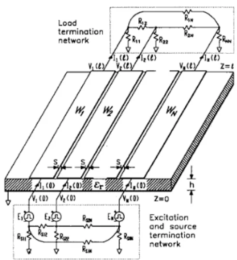
THE CORRESPONDING CHARACTERISTIC ADMITTANCE MATRIX Consider the interconnecting MCML’s with linear time- invariant source and load termination networks shown in Fig. 1 . In the termination network, the resistors are designed as R i j , where 1
5
i5
j5
N . Throughout this paper, Rii connects the end of the ith conductor to ground and R;j,i
<
j , bridges the terminals of the ith and the jth lines. It is known that N-conductor (and one ground line) MCML’s support N dominant modes. Through the full-wave solution, we can obtain an N xN
matrix[MI]
of which each column vector consists of the total current on each line for a given mode. The total current on a certain line for a given mode is defined as the area of current distribution function on that line. In this way, based on the orthogonality of modal current and voltage vectors [13], a matrix[ M v ]
is uniquely defined by[Mvl
=([Pl[MIl-’)T
(1)where the superscript T stands for the transpose operation of a matrix, and
[PI
= diag[Pk], in which p k is the total transportedpower for mode k , k = 1, 2 , . . .
,
N . The column vectors of[MI]
([ M v ] )
are called the eigencurrent (eigenvoltage) vectors of the coupled transmission lines, and they form a complete set. The current and voltage waves at any z on the MCML’s in Fig. 1 can then be expressed as(2)
[I(z)l 1
[MI]
[QI
[K’I
-[M~l[Ql-l
fK-1
[V(z)l
=[Mvl[Ql[K+l+
[MVI[QI-~[K-]
(3)where
[Q]
= diag[exp(-j/&z)] and,&
is the phase constant of mode IC. The modal expansion coefficient vectors[K+]
and
[K-]
are, respectively, for positive-z going (incident) and negative-z going (reflected) waves. They should be solved from the following boundary conditions:+
[yGl[v(0)l = [YGl[El, (4)cngfa
RwJ; and Excitation source termination networkRsii
R i i i
Fig. 1. A system of N-conductor multiple coupled microstrip lines (MCML’s) connected with excitation and source and load termination
networks.
and
[V)l
-[YLI[V(~)I
= 101, ( 5 )where the voltage excitation vector
[E]
=[El,
Ea,. . . ,
EN].
1 is the length of the MCML’s, and
[YG]
and[YL]
are the admittance matrices of the source and load networks, respectively. After[K+]
and[K-]
for each sampled frequency are determined, the propagating waveforms can be obtained from the inverse discrete Fourier transform (IDFT) of the frequency-domain data obtained by (3).The characteristic admittance matrix for the hybrid-mode MCML’s has been given by [13], [14]
[El
= [MIl[MVl-l=
[MI]
[PI
- [MI]*. ( 6 ) It can be seen that[Yc]
is symmetric and the important aspect of reciprocity is guaranteed. Note that when N = 1, ( 6 ) is the characteristic admittance of a microstrip line based on the power/current definition. Once the full N x N characteristic admittance matrix[Yc]
is specified, the values of the resistors in the MTN can be obtained as in [ 1 1 1and
Rij =
(-[Y,]ij)-l,
1 5
i<
j5
N . (8)Any termination network with admittance matrix
[YL]
not equal to[Yc]
will cause reflections, i.e.,[K-]
#
[O]. In ( 3 ) , atz =
I,
the incident voltage wave vector[V,,,]
=[ M v ]
[Q]
[K+]
and the reflected voltage vector
[Vref]
= [Mv][Q][K-] can be related by an N x N voltage reflection matrix [ p ~ ] [ 121 viaIEEE TRANSACTIONS ON MICROWAVE THEORY AND TECHNIQUES, VOL. 42, NO. 6, JUNE 1994
1010
Substituting (2), (3),
(3,
and (6) into (9), we obtain[PVI = ([YCI
+
[yLI)-l([ycl - [ Y L I ) . (10) Note that the expression of [ p v ] is identical to that for the quasi-TEM case derived in [12]. Each entry in [ p v ] indicates the relative partial reflection on one line due to a signal launched at the terminal of the same or another line. For example, [ p v ] 1 3 is the relative partial reflection on line 1 from the launched signal at the terminal of line 3. Thus, (10) can be used to measure the matching quality of termination networks. Note that the design of the MTN, and thus the reflection matrix [ p v ] , is independent of the length of MCML's.Analogous to 1121, the voltage transmission matrix [Tv] =
[U]
+
[ p v ] , where [U] is the N x N identity matrix, can be obtained asThe meaning of each entry of [Tv] can be understood from that of [pv].
The electromagnetic propagation characteristics of lossless N-conductor microstrip lines can in general be defined by an equivalent capacitance matrix [C] and an equivalent induc- tance matrix [L] which are symmetric and dispersive 1151, [16]. Substitution of (1) through (3) into the telegrapher's equations, [12], leads to
(12) where w is the angular frequency. The equivalent inductance matrix [L] can be obtained in a similar fashion.
[CI = [MI] diag (Pk/W)[P]-l[MI]T
111. CAPACITIVE COUPLING AND VALUES OF
RESISTORS IN MTN VERSUS INTERLINE SPACING As can be seen from (12), the capacitive coupling depends on the modal phase velocities and the current coupling on conducting lines. Note that the difference among the modal phase velocities is the dominant factor that causes the cross coupling [2]. In particular, when all the dominant modes have the same phase velocity, the equivalent capacitance matrix becomes the characteristic admittance matrix divided by a scalar constant, the phase velocity. In this section, we examine the relationship between capacitive coupling and a) the difference among modal phase velocities and b) the design of the MTN of a system of MCML's.
All the circuit parameters for the MCML's analyzed in this paper are computed using the standard SDA, which incorporates a set of basis functions consisting of complete charge expansion functions for a two-dimensional conducting edge [17]. This set of basis functions is capable of pro- viding accurate modal parameters, including the propagation constants and the characteristics impedances, for planar and quasi-planar transmission lines even when the conducting strips are strongly coupled.
A. Capacitive Coupling and the Interline Spacing of Coupled Microstrip Lines
For symmetric coupled microstrip lines, two fundamental propagating modes are supported, namely, even- and odd-
modes. If the characteristic admittance Ye
(Yo)
and the prop- agation constant ,Be(Po)
are known for even- (odd-) mode excitation, the equivalent capacitance matrix can be obtained from (12) as follows:1 P e Y e
+
P o y o P e Y e - P o y o Pe Y e+
P o y o[CI = -
[
2~ P e Y e - P o Y o
Let K~~ = -[CIl2 and K~~ = [C]11+[C]12. ~ 1 2 ( ~ 1 1 ) specifies the capacitance per unit length or capacitive coupling between line 1 and line 2 (line 1 and ground) 1111. For the case of layered coupled lines shown in 12, Fig. 91, the cross coupling
produced by a narrow Gaussian pulse is minimized by the substrate compensation technique. In this structure, the top layer substrate has E, = 9.7, height h2 = 0.97 mm, strip
width W = 1.5 mm and interline spacing S = 3 mm. A
second dielectric layer, thickness hl = 0.53 mm and E , = 2.2,
is inserted between the top substrate and ground to make that
Pe
=Po
= 2.161C0, where IC, is the wavenumber of free space. The characteristic impedances, based on the power/current definition, are found to be Y;' = 44 R and Y;' = 34 0. Calculation of (13) gives that ts12 = 1 . 2 ~ ~ and ~ 1 = 1 1 4 ~ , , where E , is the permittivity of free space. When S is decreasedto 0.15 mm (one tenth of W ) ,
Pe
andPo
are found to equalized at 2.31C0 using hl = 0.33 mm and h2 = 1.17 mm, and Y;' andY;' are 74 R and 27 0, respectively. Thus, ~ 1= 2
lo&,
and ~ 1= 1 1 2 ~ ~ . This proves that the capacitive coupling between the lines always exists even when the phase velocities for different modes are equalized, and that the closer the coupled lines, the larger K ~ ~ .B. The MTN for Three-Line Coupled Microstrips
It is necessary to understand the complete MTN before a de- sign for a realistic termination network with satisfactorily low reflection can be developed. For a single isolated microstrip line, the proper termination is its characteristic impedance. Let it be denoted by R,. For N-line coupled microstrips, the MTN consists of N ( N
+
1)/2 resistors, of which the values can be obtained using (7) and (8). If the interline spacing is sufficiently larger than the maximum strip width, an adequate approximation is to use the microstrip impedance of the ith line as R;; and to ignore all the Rij's,i
<
j . As the strips are placed closer, the capacitive coupling among the strips is increased and the resistance values may change greatly. Thus, in this subsection, we turn to investigating the design of the MTN for an N-conductor microstrip structure for different interline spacing.Fig. 2(a)-(c) plot the circuit parameters for a three-conductor coupled microstrip structure against S / h , for W / h = 0.2 and 2, at 5 GHz and 50 GHz. The three equally spaced microstrips have identical line width.
Fig. 2(a) plots the normalized phase constants of the three fundamental modes for S / h from 0.01 to 10. The largest separations among the normalized phase constants (and thus the modal phase velocities) occur when W / h = 2 and
S / h
<
0.1. More cross coupling will occur when a narrow pulse propagates along MCML's with these ratios. The leastKUO AND TZUANG: A TERMINATION SCHEME FOR HIGH-SPEED PULSE PROPAGATION 101 1 - 2.5 3.5 W/h=2 0 W/h=0.2 I I I I I I l l 1 I I I I I I I I I I I I I I I l l 5 GHz .... - 50GHz 3 1 I I I I I I l l I I I I I I I I I I I I I I I I I I 50GHz - d --2 2 \ Orc K 2 1 0 0 1 0 0 2 0 0 5 0 1 0 2 s / h 0 5 1 2 5 10 20 18 16 14
-
50GHz 2 1 2>
S l O $ 8 6 4 2 0 0 0 1 0 0 2 0 0 5 0 1 0 2 s / h 0 5 1 2 5 10 (C) Flg 2matched termination network (MTN) (b) c y 1 1 = R I I / R , and cy22 = R22/Rp. and (c) cy12 = Rlz/R,, and a13 = R I ~ / R , ,
(a) Normalized phase constants of the dominant modes for the symmetnc three-conductor mcrostrip lines Normalized values of resistors of the
separation occurs at 5 GHz for W / h = 0.2. This suggests that, as expected, using narrow conducting microstrips and pulse of longer rise time can effectively maintain the quality of propagating signal along lengthy coupled lines.
Fig. 2(b) and (c) plot the normalized resistance values aij = R;j/R, of the resistors used in the MTN for the MCML’s. The values of R, are 78.9 R (29.3 R) and 84.1
R
(31.7 0) at 5 GHz and 50 GHz, respectively, for W / h = 0.2 ( W / h = 2). The computation of R;j’s, i, j = 1, 2 or 3, is based on (6), (7), and (8). Due to the symmetry of the three-line structure: all = a33 and a12 = a 2 3 . Thus only all and a 2 2 [plotted in Fig. 2(b)], and a12 and a13 [in Fig. 2(c)] need to be specified. In Fig. 2(b), when W / h = 2 and S / h<
0.2, connections to ground in the MTN require resistors with more than 20% of the value of R, for the outermost lines, and a resistor with more than 50% of R, value for the central line. The values of a 2 2 . for W / h = 0.2, decrease markedly as the interline spacing increases. In Fig. 2(c), for tightly packed structures ( S / h<
0.1), R12 for each case has a value comparable with that of R, when S / h5
1 and R13 has nearly six times the R,values. Note that values of a13 for W / h = 2 are not plotted as they exceed the scale used here.
R;j’s, i
<
j, in the termination network are connected in a parallel sense. When S is less than h, Rl2 has a small value and thus it will have significant effect on the quality of received signal. However, when S / h 2 0.5 ( S / h2
3), the connection of R13 (R12) becomes unnecessary. Note that, at these values of S / h ratios, values of R;;’s are still required to be slightly larger than that of R,, and that the change in frequency has the most effect on the R12 and R13 values, but as they are not required, the effect is of no importance.As indicated in the example given in the last subsection, when the interline spacing of the coupled strips is decreased, the capacitive coupling of each line with respect to ground decreases, and the values of R11 and R22 increase. The decrease in capacitive coupling for the central line is greater than that for the outer lines and thus R 2 2 2 R11 2 R, as shown in Fig. 2(b). At the same time, the value of R12 as seen in Fig. 2(c) decreases because the capacitance per unit length between lines 1 and 2 increases. For the 50 GHz case,
1012 IEEE TRANSACTIONS ON MICROWAVE THEORY AND TECHNIQUES, VOL. 42, NO. 6, JUNE 1994
the interline coupling is larger, thus a 1 2 and a13 are lower than that for 5 GHz. Note that the propagation constants and the values of the termination resistors for the MCML's converge to those of a single isolated microstrip line when S / h
>>
W / h .Iv. CROSS COUPLING PRODUCED ON
TIGHTLY COUPLED MICROSTRIP LINES
A dispersive database of modal phase constants and [ M I ]
and [Yc] matrices is required for computing the waveforms propagating along terminated MCML's. To save CPU time, the piecewise-linear approximation used in [4] is applied to simulate the frequency-dependent data. Before applying the IDFT (Inverse Discrete Fourier Transform) to the data obtained in (3), it should be noted that the maximum frequency of the sampled data should be large enough to obtain sufficient time-domain resolution of the propagating waveforms, and that the incremental frequency of the complete database must not exceed the reciprocal of the total elapsed time for the pulse traveling from the source to the receiving end.
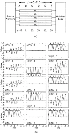
The propagating waveforms on each line of a system of tightly coupled five-conductor microstrips in response to three sets of excitations are used to evaluate the level of cross coupling. The circuit schematic is shown in Fig. 3(a) and the propagating waveforms in Fig. 3(b). Each column in Fig. 3(b) depicts one set of excitations and every excitation within each set is denoted by a character, A. The propagating waves are
observed at z = X, 2X,
. . . ,
and 5X, and denoted, respectively, by characters B, C,. . .
and F, where X is the average guided wavelength of the fundamental modes forf
= ( 0 . 3 5 / t , ) GHz, the 3 dB bandwidth of a step signal with rise timet ,
in ns [18]. The source impedances are short-circuited and the load end is perfectly matched. As there is no reflected wave, the degradation of the propagating waves is entirely due to dispersion and cross coupling.For the five-conductor coupled microstrips, five dominant modes exist. These modes have eigencurrent vectors with relative signs
(+++++),
( + + O - - ) , (+---+), (+-+- +), and (+ - 0+
-), and are designed as M l 1 M 2 , ..
. I Ms,respectively. Their corresponding normalized phase constants are, at 10 GHz, 2.9117, 2.6551, 2.6372, 2.6368, and 2.6367. Since the structure is symmetric, the magnitudes of the first and the second entries of each eigencurrent vector are identical to those of the fifth and the fourth entries, respectively.
In column 1 on the left-hand side of Fig. 3(b), a pulse is excited on line 1. The cross coupling or crosstalk on the inactivated lines increases as the pulse propagates away from the source. In column 2, lines 2 and 4 are excited by pulses with opposite polarities. Due to symmetry, only modes M2 and M5 are activated. Since the phase velocities of these two modes have close values, the pulses have negligible distortion when they arrive at the receiving end. In column 3, three in- phase pulses are excited on lines 1, 3, and 5, and thus only modes M I , M3, and M4 are activated. Since the value of the
phase constant for M I departs from those for M3 and M4,
significant crosstalk is inevitably produced. As a result, the
peak amplitude of the composite crosstalk on lines 2 and 4 at the load end exceeds 70% of that of the excited pulses.
Source Vetwork +--- 1=40.615mm--cl A B C D E F F ! Matched z=O 2h 3A 4 h 5h (a) -.El , , , , ,
1
1
, , , , ,1
/LINE, 5 , , ,1
-1.2 -.ElI
t
4t
1 A B C L E F,p y
t L I N E , 3 , , ,1
"'ILINE, 1 , , ,1
I L I N E , 1 , , ,1
[LINE, 1 , , ,1
-1.2 0 .1 .2 .3 .4 .5 .6 0 .1 .2 .3 .4 .5 .6 0 .1 .2 .3 .4 .5 .6 (4 (4 ( n 4 (b)Fig. 3. High-speed pulses propagating along a system of closely coupled five-conductor microstrip lines. (a) Circuit schematic. (b) Propagating wave- forms observed at various distances along the lines in response to three sets of excitations. Structural parameters: W1 = Wz = ... = W5 = W, W / h =
10S/h = 0.2, h = 0.1 mm and er = 12.9. Waveform parameters:
t , (0% - 100%) = t,(lOO% - 0%) = 25 PS, tw = 100 PS.
As indicated in Fig. 3(b), the signals are more deteriorated as the distance from the source increases. It can be concluded that, for any excitation, when the MCML's are electrically short, the distortion of propagating pulses caused by dispersion and cross coupling becomes negligible, even if the lines are tightly coupled. Thus, proper design of the termination network becomes the most important factor if good power delivery from the source to the load is to be achieved.
The ideal termination for the five-conductor coupled mi- crostrips is its MTN, since no reflection will occur. Unfor- tunately, in planar MMIC fabrication, it is nearly impossible to build the complete MTN, as it requires fifteen resistors to connect each terminal of every conductor to ground and to one another. Thus, we are motivated to design a realistic termina- tion scheme for the tightly coupled MCML's that will have
KUO AND TZUANG: A TERMINATION SCHEME FOR HIGH-SPEED PULSE PROPAGATTON 1013
both satisfactorily low reflection and practical realizability in the planar MMIC environment.
v.
THE PROPOSED REALISTIC TERMINATION SCHEMEFOR PLANAR MMIC AND THE COMPARISON OF REELECTIONS DUE TO IMPERFECT TERMINATIONS This section evaluates the effect of four termination net- works on the quality of the received signal. The four networks fall into two types of circuit schemes. The first type of scheme has only resistors connecting line terminals to ground, and its admittance matrix is diagonal. This type of termination is attractive not only for the ease of fabrication, but also for the simplification of the transient analyses of multiple coupled transmission lines [9]. The first termination network inves-
tigated (admittance matrix [Y,d;ag]) uses the characteristic impedance of a single isolated microstrip line (R,) as
Ri;,
1
5
i5
5. However, since these values may not give the best result, it is necessary to investigate whether the reflection performance can be improved if the resistance values are op- timized. The second termination network devised (admittance matrix [Yopdiag]) is constructed using these optimal resistors. The optimized resistance values are obtained by minimizing5 5
s,
= y ~ I [ P v I i j l 2 (14) i = l j = 1where the voltage reflection coefficient matrix [ p v ] is calcu- lated using (10).
The second type of circuit scheme is the proposed scheme. Resistors are used to connect each line terminal to ground and to the nearest adjacent line terminals. The realization of this type of circuit scheme needs no via, air-bridge or any vertical implementation of the resistors, if all the coupled microstrip lines are placed in the same dielectric-dielectric interface. [Yprop] is the admittance matrix of the third termination network which uses Rij, li - j l
5
1, of the MTN evaluated at ( 0 . 3 5 / t , ) GHz, while the otherai’s,
li-
j l2
2, are left open circuited. The resistance values of this type of circuit scheme can also be calculated using (14). It forms the fourth termination network and its admittance matrix is designated as[Yopprop].
Note that, as seen in Fig. 2(c), the values of Rij’s forli-jl = 2 of the MTN decrease, and their importance increases
as W / h is decreased. They, however, are not included in this type of termination scheme. Therefore, the test case, i.e., W / h = 10S/h = 0.2, creates a crucial examination of matching quality of the proposed termination scheme.
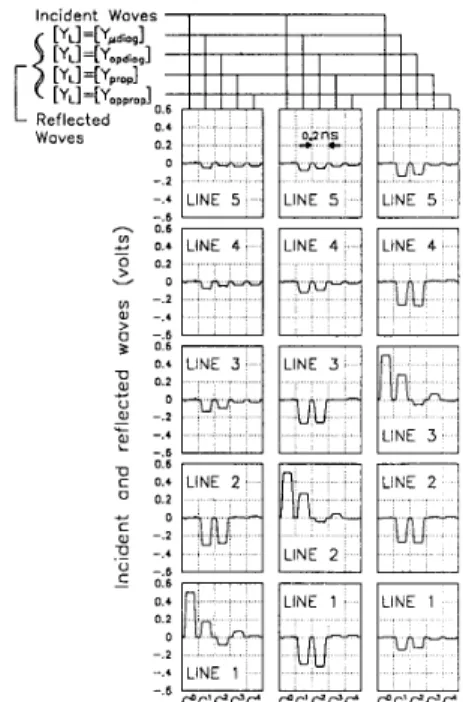
Fig. 4 plots the incident and reflected waves on the tightly coupled five-conductor microstrips terminated in the four load networks. There are three columns and each of them corresponds to one set of excitation. Each column has time slots denoted by C:, where 1
5
i5
3 and 05
j5
4, and the subscript i specifies the order of the column. The incident waves to the load are plotted in the slots denoted by j = 0. The reflected waves drawn in time slots C:with j = 1, 2, 3, and 4 correspond to the four termination
networks with admittance matrices [Ypdiag], [Yopdiag], [Yprop], and [Yopprop], respectively.
Incident Waves
$
!q--+qM
;
!;HMM
;;MHH
wl - 2 w - I 0 - 6y---q-qv
w - 2 Y - LINE 3 c E - 4 - 6 +. p - 4 LINE 2 - 2 - 4 LINE 1 - 6 CCdCC: CGCdc:cc:cm
Fig. 4. Comparison of reflected waves created by the four imperfect termination networks. Each reflected wave is multiplied by a factor of 2. The length of the MCML’s is 3 mm, and the other circuit parameters are referred to those used in Fig. 3 In the load network [Y,dzag]. R,, = R , = 77 00 R for 1 5 z 5 5, and R,, = 00 for 2 # 3 ; [Yopdzag]: R11 = 41.83 R, R22 = 35 61 12, R33 = 33.78 f2, and R,, = 00 for z # 3; [Yprop]. R11 = 145.1 R, R12 = 68.74 R,
R22 = 279.7 0, R23 = 72.95 0 , R33 = 303.8 R and R,, = 00 for
R23 = 62.46 R, R33 = 274.5 R. Note that due to the symmetry of the structure: R11 = R55, Rlz = R45, R22 = R44, and R23 = R34. 12-31 2 2 ; [YopprOp]: R I I = 133.6 0, Ri2 = 61.77 Q, Rz2 = 268.4 R,
The length of the MCML’s is 3 mm, which approximates the maximal length of the interconnects in an MMIC. The source impedance is perfectly matched to obtain the least distorted waveform at the sending end. In columns 1 through 3, a pulse is excited on lines 1, 2, and 3, respectively, at the source end. All the excited pulses begin at
t
= 0, and each waveform plotted in any C l slot starts att
= 0 and ends at 0.2 ns. All the reflected waves are multiplied by a factor of 2 for better identification.Examination of the waveforms gives an indication of the magnitude of crosstalk and reflection which occurs for dif- ferent terminations. It can be seen that the cross-talk has negligible magnitude. The reflected pulses are significantly reduced on the signal lines when the termination [Ypdiag] is replaced by [Yopdiag], but not on the neighboring lines. The proposed termination scheme ( [Yprop], [Yopprop]), however, produces a significant reduction in the ,reflected signals on both excited and neighboring lines. In Ci, Ci, and Ci, j = 3
and 4, the reflections on signal lines are further improved if the termination [Yopprop] is used instead of [YprOp]. On inactivated lines, however, [Yprop] has better reflection performance.
As indicated in Fig. 4, the reflection on each line of the MCML’s depends on which line is activated. To compare the reflection performance of the four termination networks, the worst or the maximal reflection on each line for arbitrary
1014 IEEE TRANSACTIONS ON MICROWAVE THEORY AND TECHNIQUES, VOL. 42, NO. 6 , JUNE 1994
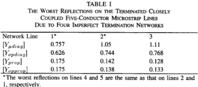
TABLE I
THE WORST REFLECTIONS ON THE TERMINATED CLOSELY
COUPLED FIVE-CONDUCTOR MICROSTRP LINES
DUE TO FOUR IMPERFECT TERMINATION NETWORKS
Network Line 1' 2* 3
[ Y o p d z a g l 0.626 0.744 0.768
[ Y p r w l 0.175 0.142 0.128
[Yoppropl 0.175 0.138 0.133
*The worst reflections on lines 4 and 5 are the same as that on lines 2 and
1, respectively.
[ Y ~ d z a g l 0.757 1.05 1.11
combination of signal sources is also examined. Due to the symmetry of the structure, the reflected waves in response to the excitations on lines 4 and 5 can be known from those on lines 2 and 1, respectively. For example, the reflection on line 2 due to the excitation on line 5 is identical to that on line 4 due to the excitation on line 1. Since the terminated MCML's system is linear, the reflected wave on
any line for arbitrary excitation is a weighted sum of those in Fig. 4, with the weighting coefficients being the amplitudes of the excitations. The results are listed in Table I. Here, the transmitted digital signals on each line may make excursions between +1 (volt) and -1 (volt) corresponding to logic-1 and logic-0, respectively. Thus, the worst reflection on line IC, 1
I
IC
I
5 , is the sum of the absolute values of reflected waves in response to each $1 input on lines 1 through 5. Note that the maximal reflections on different lines for each termination network may occur for different combinations of signals at the sending end.According to Table I, the maximal reflection caused by the network [Yopdiag] shows at least a 25% improvement over that caused by the network [Ywdiag]. The magnitude of reflection may be greater than 60% of the input signal for the first type of termination scheme (
[Ypdiag],
[Yopdiag]). For the proposed scheme, both termination networks ( [Yprop], [Yopprop]) have close values for the worst reflection on every line. The maximal reflection caused by the proposed termination scheme is 17.5% which is near or at least four times smaller than that produced by the first type of termination..VI. MEASUREMENT RESULTS
A system of tightly coupled six-line microstrips terminated in a load with admittance matrix [Yprop] is measured to verify the reflection performance of the proposed termination scheme. The measured circuit is fabricated on an alumina (Al2O3) substrate which is firstly -coated with a Tantalum Nitride (TaN) thin film resistive layer and then secondly with metal. The area of each TaN pad is made as small as possible to minimize nonideal effects, such as parasitic capacitance at high frequencies.
Fig. 5(a) shows the circuit schematic and parameters of the measured six-line microstrips. The test circuit is assumed to be lossless and designed to have enough length to assure a sufficient separation in time between waveforms of successive multiple reflections at each port. All the resistor values are measured at dc. Note that all the source impedances are short- circuited, except for the line used as port 1. The width of line
IC 1 = 18.44mm -4 R i ~ 3 2 . 8 n S=0.254m m Rzz=31.20 h=0.254mm Ris=50.0n W ~ 0 . 6 3 5 m m Riz=266fl MLF0.762" wz S Rz3=294R wF0.416mm W, R34=323fl &,= 9.9(AI24) -.l
I
0.1,
I 0.0 -.l - 7 .- -.2 -.l 0 0.1 0.2 0.3 0.4 0.5 0.6 0.7 0.8 0.9 1.0 (ns) (b)Fig. 5. (a) Circuit schematic and parameters of the measured closely coupled six-line microstrip structure. (b) Measured and theoretical Szl and SII
responses.
3 is chosen via (6) and (7) so that R33 is 50 R, which matches the impedance of the coaxial cable of the HP8510B.
Fig. 5(b) consists of plots of the measured and theoretical time-domain responses of S l l and Sal as well as a time- space diagram. The waveform (A) is the input signal at port 1. Since the input impedance of port 1 is not 50 R, it inevitably produces a reflection (B) at t = 0. The received signal at port 2, waveform (C), is a sum of the incident and reflected
waves. The Szl plot of this waveform indicates that the coupled microstrips introduce a 0.01 dB/mm loss to the signal. Except for the loss, the measured result has good agreement with the theoretical waveform. This shows that the theory of multiconductor transmission lines based on the reciprocity relation has been correctly applied to the analyses of pulse transmission along the closely packed MCML's.
The reflected part (C') of waveform (C) will travel toward
the source end for t
>
166 ps, where it is designated as (D'). The waveform (D') is close to waveform (C'), since the testMCML's are so electrically short that the distortion caused
by dispersion and cross coupling is negligible. To obtain waveform (D) from (D'), the transmission matrix [Tv] can be invoked. It can be shown that [Tv] = 2[Zs][Yc]([U]
+
[Zs][Yc])-', where [Zs] and [VI are the source impedance and the identity matrices, respectively. Since [ Z , ] has only one nonzero entry [Zs]33 = 50 Q, one can verify that [Tv] has null entries in all the rows other than the third one, and [Tv]3lc = 2[Yc]3k/([Yc]33
+
([Zss]33)-'), 1I
I
6 .KUO AND TZUANG: A TERMINATION SCHEME FOR HIGH-SPEED PULSE PROPAGATION 1015
The signal (D) is the sum of products of [T~7]31~ and the corresponding incident wave on line
k.
In other words, port 1 collects the reflected waves (C’) on line 3 and on the other lines from the load end. Both the theoretical and measured results show that the peak amplitude of reflection is below -30 dB (3%).VII. CONCLUSION
Various termination networks have been examined to deter- mine a design that gives satisfactorily low reflection and good practical realizability when implemented in a planar MMIC. An analysis of the matched termination network (MTN) for a three-conductor hybrid-mode coupled microstrip structure is reported. A study of high-speed pulses propagating along a system of closely coupled microstrip lines is also presented. It is found that when the coupled transmission lines are electrically short, the only concern for good power delivery from the source to the load becomes the proper design of the termination network.
Reflections produced by four termination networks applied to a tightly coupled five-conductor microstrip interconnecting system (line width:interline spacing = 10: 1) have been studied extensively. A termination network which consists of only terminal-to-ground resistors can cause signal reflection of greater than 60%. The proposed termination scheme produces at worst a reflection of 17.5%. The measured responses for a six-line microstrip circuit verify the proposed concept for terminating a tightly coupled coplanar N-conductor microstrip structure for use in the planar MMIC environment.
ACKNOWLEDGMENT
The authors would like to thank L.-K. Chang, H.-S. Huang,
and M.-H. Lin at MTI and K.-S. Hsu and his colleagues at CSIST for their help in fabricating the measured multiple cou- pled microstrip circuits. S. Cheng’s assistance in performing the measurements is also much appreciated.
REFERENCES
K. K. Li, G. Arjavalingam, A. Dienes, and J. R. Whinnery, “Propagation of picosecond pulses on microwave striplines,” IEEE Trans. Microwave
Theory Tech., vol. MTT-30, pp. 1270-1273, Aug. 1982.
J. P. K. Gilb and C. A. Balanis, ‘‘Pulse distortion on multilayer coupled microstrip lines,” IEEE Trans. Microwave Theory Tech., vol. 37, pp. 1620-1627, Oct. 1989.
J. P. K. Gilb and C. A. Balanis, “Asymmetric, multi-conductor low- coupling structures for high-speed, high-density digital interconnects,”
IEEE Trans. Microwave Theory Tech., vol. 39, pp. 2100-2106, Dec.
1991.
L. Carin and K. J. Webb, “Isolation effects in single- and dual-plane VLSI interconnects,” IEEE Trans. Microwave Theory Tech., vol. 38, pp. 396404, Apr. 1990.
E. G. Farr, C. H. Chan, and R. Mittra, “A frequency-dependent coupled- mode analysis of multiconductor microstrip lines with application to VLSI interconnection problems,” IEEE Trans. Microwave Theory Tech., vol. MTT-34, pp. 307-310, Feb. 1986.
R. Wang and 0. Wing, “A circuit model of a system of VLSI intercon- nects for time response computation,” IEEE Trans. Microwave Theory
Tech., vol. 39, pp. 688-693, Apr. 1991.
L. Carin and K. J. Webb, “An equivalent circuit model for termi- nated hybrid-mode multiconductor transmission lines,” IEEE Trans.
Microwave Theory Tech., vol. 37, pp. 1784-1793, Nov. 1989.
S. Seki and H. Hasegawa, “Analysis of crosstalk in very high-speed LSWLSI’s using a coupled multiconductor MIS microstrip line model,”
IEEE Trans. Microwave Theory Tech., vol. MTT-32, pp. 1715-1720,
Dec. 1984.
H. You and M. Soma, “Crosstalk and transient analyses of high-speed interconnects and packages,” IEEE J. Solid-state Circuits, vol. 26, pp. 319-329, Mar. 1991.
C.-K. C. Tzuang and T. Itoh, “High-speed pulse transmission along a slow-wave CPW for monolithic microwave integrated circuits,’ IEEE
Trans. Microwave Theory Tech., vol. MTT-35, pp. 697-704, Aug. 1987.
H. Amemiya, “Time-domain analysis of multiple parallel transmission lines,” RCA Rev., pp. 241-276, June 1967.
K. D. Marx, “Propagation modes, equivalent circuits, and characteristic terminations for multiconductor transmission lines with inhomogeneous dielectrics,” IEEE Trans. Microwave Theory Tech., vol. MTT-21, pp. 4 5 M 5 7 , July 1973.
L. Wiemer and R. H. Jansen, “Reciprocity related definition of strip characteristic impedance for multiconductor hybrid-mode transmission lines,” Microwave an Opt. Tech. Lett., vol. 1, pp. 22-25, Mar. 1988. G. W. Slade and K. J. Webb, “Computation of characteristic impedance for multiple microstrip lines by using a vector finite element method,”
IEEE Trans. Microwave Theory Tech., vol. 40, pp. 3 4 4 0 , Jan. 1992.
V. K. Tripathi and H. Lee, “Spectral-domain computation of character- istic impedances and multiport parameters of multiple coupled lines,”
IEEE Trans. Microwave Theory Tech., vol. MTT-37, pp. 215-221, Jan.
1989.
S. Amari, “Capacitance and inductance matrices of coupled lines from modal powers,” IEEE Trans. Microwave Theory Tech., vol. 41, pp. 146-150, Jan. 1993.
J.-T. Kuo and C.-K. C. Tzuang, “Complex modes in suspended coupled microstrip lines,” IEEE Trans. Microwave Theory Tech., vol. 38, pp. 1189-1 197, Sept. 1990.
P. R. Gray and R. G. Meyer, Analysis and Design of Analog Integrated
Circuits. 2nd ed. New York: Wiley, 1984, ch. 7.
Jen-Tsai Kuo (S’89-M’93) received the B.S. de- gree in communication engineering from the Na- tional Chiao Tung University (NCTU) in 1981 and the M.S. degree in electrical engineering from the National Taiwan University in 1984, both in Taiwan, R.O.C.
Since August 1984, he has been with the De- partment of Communication Engineering at NCTU as a lecturer at the Microwave and Communication Electronics Laboratory. From September 1988 to June 1992, he worked on the Ph.D. degree under the guidance of Prof. Ching-Kuang C. Tzuang. His research interests include the field-theoretical study of guided waves, analysis and design of active and passive microwave circuits and high-speed interconnects and packages, and numerical techniques of applied electromagnetics.
Ching-Kuang C. Tzuang (S’84-M’86-SM’92)
was born in Taiwan on May 10, 1955. He received the B.S. degree in electronic engineering from the National Chiao Tung University, Hsinchu, Taiwan, in 1977, the M.S. degree from the University of California at Los Angeles in 1980, and the Ph.D. degree in electrical engineering in 1986 from the University of Texas at Austin, where he worked on high-speed transient analyses of monolithic microwave integrated circuits.
From February 1981 to June 1984, he was with TRW, Redondo Beach, CA, working on analog and digital monolithic microwave integrated circuits. Since September 1986, has been with the Institute of Communication Engineering, National Chiao Tung University, Hsinchu, Taiwan, R.O.C. His research activities involve the design and development of millimeter-wave and microwave active and passive circuits and the field theory analysis and design of various quasi-planar integrated circuits.