In the integrated circuit (IC) fabricating process, a suitable sur- face treatment in addition to standard RCA cleaning is required to completely remove contaminants of organic materials or metallic ions contained in the native oxide and reduce surface microrough- ness. It is well known that surface microroughness at the SiO2-Si interface has a significant effect on the electrical properties of metal- oxide-semiconductor (MOS) devices as gate oxide scales down to nanometer size.1 A silicon surface with no native oxide and full hydrogen-passivated surface is an important issue to be assured of high breakdown field, high charge to breakdown, and low leakage current.1,2In the literature, a promising dry cleaning technology of plasma etching was shown to remove oxygen from the Si surface ef- fectively, as well as improve charge to breakdown; however, the Si surface was roughened with plasma-damaged lattices.3-6 Other newly developed dry cleanings, including laser cleaning for the re- moval of surface particles,7gas-phase surface cleaning using anhy- drous HF/methanol, UV/Cl2, and UV/O2,8,9in situ cleaning in a hy- drogen ambient at atmospheric pressure using HF and HCl gas,10 and Cl radicals generated with UV irradiation,11were investigated.
These dry cleaning methods showed effective removal of submicron particles,7 native oxides,9,10and Fe contaminants.11 Nevertheless, dry cleaning showed inferior performance, for example, for Ca removal and surface microroughness,8 in comparison with wet cleaning. As an alternative, a convenient method of cleaning tech- nology based on H2O2chemistry in semiconductor manufacturing process has been demonstrated to be the most efficient wet cleaning method before the growth of thermal oxide. Many novel wet clean- ing methods have been proposed in the literature, such as HF/deion- ized (DI) water/O3/megasonics cleaning,12 ozonized water/diluted HF,13 modified RCA cleaning,14 HNO3-HF system,15,16 HF-last cleaning process,17and HF-H2O2system,18which were utilized in addition to the standard RCA cleaning process. It was shown that low surface microroughness and a high degree of surface passivation were achieved and consequently the oxide quality of thermally oxi- dized silicon was remarkably improved.
In this paper, the effects of various surface treatments (or clean- ing processes) are investigated to clarify the improvement of oxide- Si interface and oxide quality of liquid-phase deposited fluorinated silicon oxides (LPD-SiOF). In the previous works of the LPD method, it can be summarized that (i) dilute hydrofluoric acid was used to remove the native oxide in addition to RCA cleaning19-23;
(ii) a combination of acetone and methanol followed by a HF dip was used to initially clean Si substrates.24Breakdown fields as high as 8-9 MV/cm and average interface trap density of 1011eV21cm22 were achieved. However, to our knowledge, no similar study for the effect of surface treatment on LPD-SiOF films has been proposed.
Because the oxide growth mechanism of LPD-SiOF (i.e., deposi- tion) is different from that of thermal oxide25(i.e., oxidation) but much similar to chemical vapor deposited (CVD) oxide, the inter- face property is unavoidably affected by the degree of surface clean- liness. For the consideration of thin oxide growth, surface micro- roughness and surface passivation would both affect the oxide qual- ity in LPD oxides. In this study, some etching solutions were pre- pared after the standard RCA cleaning to etch the native oxide formed during RCA cleaning. A detailed and complete oxide growth mechanism was suggested in relation to surface treatments since interface properties are strongly dependent on surface morphology.
Oxide quality improvements including breakdown field and average interface trap density after various surface treatments were investi- gated. Moreover, it has been widely used in semiconductor manu- facturing processes of high temperature thermal annealing to densi- fy the oxide films. A high temperature thermal annealing, such as N2 furnace annealing,19 rapid thermal oxidation (RTO),26O2 and H2 plasma,27and rapid thermal nitridation (RTN)28tends to alter the oxide bonding characteristics, leading to a denser oxide network and/or strengthening of Si-O bonds near the oxide-Si interface by re- ducing oxygen vacancies. Therefore RTA is also employed in this study to drive fluorine out of LPD oxides and densify LPD-SiOF films since this is an effective and rapid annealing for future ultra- large scale integrations (ULSIs). It was found that oxide breakdown field and interface properties were clearly improved.
Experimental
n-Type silicon wafers with (100) orientation and resistivity of 9- 12 V-cm were used as the substrates. For RCA cleaning, substrates were boiled in an APM solution (NH4OH/H2O2/H2O) with a volume ratio of 0.05:10:50 at 808C for 15 min to remove organic materials on the started substrates. The smaller content (i.e., 0.05) of NH4OH other than that (i.e., 10) in conventional RCA cleaning has been demonstrated to greatly reduce the surface microroughness.14After dipping APM-treated substrates into ultraclean DI water for 5 min, they were subjected to HPM solution (HCl/H2O2/H2O) with a vol- ume ratio of 10:10:60 at 808C for 15 min to remove alkaline ions and metallic ions. These substrates with chemically formed native oxides
Effect of Surface Treatments on the Electrical Properties of Fluorinated Silicon Oxides
W. J. Chang, M. P. Houng,
zand Y. H. Wang
Department of Electrical Engineering, National Cheng-Kung University, Tainan 70101, Taiwan
In this study, different surface treatments of HF-based etching solutions are investigated for the predeposition of liquid-phase deposited fluorinated silicon oxides (LPD-SiOF). The effects of each etching solution on the interface trap density and breakdown field are examined with Al/LPD-SiOF/Si structure. From the experimental results, there appears significant growth delay time for different surface treatments during the initial oxide deposition, which is defined as the surface modification time to reach an OH- rich surface promoting the growth of LPD-SiOF film. However, the subsequent deposition rate remains unchanged for all etching processes, indicating a surface-independent deposition process. It is found that a two-step treatment in dilute HF/H2O with 1:200 v/v ratio reveals an average breakdown field of 9.7 MV/cm and an extremely low average interface trap density (,1010eV21 cm22), which are comparable to that of thermal oxides. Moreover, the rapid thermal annealing process is suggested to clearly improve the oxide quality for this two-step etching process, where early breakdown is eliminated (18% raising for EBD) and inter- face properties are substantially improved (33% reduction for DH). The improvements for device performances are believed to be due to the oxide-free Si surface passivated with hydrogen and reduced surface microroughness (Ra5 0.1 nm). It is evident from our experiments that this new two-step surface treatment is an effective method for interface improvement with oxide deposited by LPD or chemical vapor deposition.
© 2000 The Electrochemical Society. S0013-4651(99)10-061-2. All rights reserved.
Manuscript submitted October 15, 1999; revised manuscript received May 5, 2000.
z E-mail: [email protected]
by APM and HPM were dipped into different etching solutions (see Table I) to remove native oxides completely and achieve a hydrogen- passivated surface.
Afterward, a growth solution consisting of hydrofluorosilicic acid concentration of 1.8 mol/L and DI water was prepared for LPD- SiOF to deposit on surface-cleaned substrates. The deposition tem- perature was adjusted to 308C. Details of the experimental process are in our previous study.29The surface-etched substrates were de- livered into the LPD growth system immediately to suppress native oxide growth. The thickness of LPD-SiOF film was controlled to 10 nm, which was deposited on patterned substrate. Then aluminum was deposited by thermal evaporator and lifted off. A postmetalliza- tion annealing of 4008C for 30 min in nitrogen ambient was em- ployed. As for the RTA process, the substrates were annealed at 9508C for 150 s in nitrogen ambient.
Both the as-deposited and RTA samples were delivered to capac- itance-voltage (C-V) measurement to calculate the average interface trap density, a method proposed by Jakubowski et al.30where the errors were within 5% compared to the Terman method.31A current- voltage (I-V) measurement was used to evaluate the breakdown field.
The I-V characteristics were measured by the dc ramp method with a ramp rate of 0.2 V/s and a positive gate bias. The criterion for the breakdown field was defined that a large leakage current of 10 mA/cm2 was reached or a catastrophic breakdown occurred.
Effects for various surface-etching processes on the electrical prop- erties were compared.
Results and Discussion
Characteristics of surface treatments on Si surface.—As listed in Table I, six etching solutions based on HF were utilized in this study.
The step of aqueous HF dipping is important because all native oxides formed during RCA cleaning are removed. Subsequently, a hydrogen-passivated surface can be easily formed on silicon sub- strate. A native-oxide-free surface prior to oxidation is crucial for ultrathin thermal oxide growth since the native oxide contains many pinholes and defects, and thus degrades the quality of whole oxide.1 Sample CN-1 was prepared with a short time dip (i.e., 15 s) of HF/H2O 5 1:40 and DI water rinse. Samples CN-3A and CN-3B were both dipped into HF/MeOH 5 1:10 for 30 s; however, no DI water rinse was prepared for CN-3A. The use of MeOH instead of H2O has been confirmed1for the reduction of stress-induced leakage current (SILC) and increase of dielectric breakdown and charge to breakdown because hydrogen-passivated surface and reduced sur- face microroughness were achieved. Furthermore, a rinse in DI water destroys most of the hydrogen-passivated surface, and then promotes the growth of the native oxide. Sample CN-4B received a two-step HF/H2O dipping (i.e., etched r rinsed r etched). The etch- ing processes of CN-5B and CN-6B were of similar etching solu- tions, a HNO3/HF/H2O called slight etch (SE) solution and a HNO3/HF/H2O2 called controlled slight etch (CSE) solution.15,16 After finishing the last three etching processes, the substrates were immediately dried with nitrogen blown without a DI water rinse.
These etching processes right after the RCA cleaning process tended to modify surface properties remarkably. This can be ex- plained by first noting the growth curves. As shown in Fig. 1 for the typical characteristics of oxide thickness vs. deposition time, obvi- ous growth delay time (GDT) appears during the initial growth. The GDT for CN-1 is shorter (0 min, not shown in this figure) than CN- 4B because CN-1 receives a 5 min DI water rinse. Owing to the growth of native oxide, no GDT is observed. GDT is estimated to be within 12 min when a two-step etching process (CN-4B) is used. For the same reason, CN-3B shows shorter GDT (2 min, not shown in this figure) than CN-3A because of the DI water rinse. Interestingly, no GDT is seen in CN-5B, which is believed to be due to the growth of native oxide during the etching process by the oxidized reaction of HNO3and Si.16On the contrary, CN-6B used H2O2instead of H2O to suppress the autocatalytic reaction of HNO3with Si, hence little native oxide was obtained (GDT 5 5 min, not shown in this fig- ure). Furthermore, chemical oxides formed by HNO3were etched off completely by HF because the rate-determining step was the oxi- dation of Si by HNO3. After the growth of the first atomic layer of LPD-SiOF, the deposition rate was almost the same, no matter which etching process was treated on Si substrate (i.e., surface-independent growth mechanism for LPD). It is therefore suggested that some sur- face modifications occur during the growth of LPD-SiOF for various surface treatments.
Initial LPD growth mechanism.—The explanations for GDT can be understood from the growth mechanism. Initially, the RCA-treat- ed Si surface is full of chemically formed native oxide. Subsequent dipping in HF-based etching solutions with primary species of inte- gral HF molecule leads to the fact that these molecules can easily insert themselves between Si and O of Si-O bond and leave Si-F on the sample surface.23The polar nature of the Si-F bond makes it sus- ceptible to HF attack, which frees the SiFxspecies into the solution and simultaneously forms hydrogen termination. HF-treated Si(100) surface will therefore be covered mainly by Si-H and Si-H2bonds.
The hydrogen on the Si surface will be replaced by hydroxyl through the reaction of
Si-H 1 H2O r Si-OH 1 H2
which is favorable for the growth of LPD-SiOF.32The necessity of Si-OH bonds on the substrate surface and formation of intermediate species in the LPD growth solution are common features because the intermediate polysilcic acid is formed by the polymerization of sili- cic monomer Si(OH)4, where two different intermediate species, SiFm(OH)42mand (SiF6?SiF4)22, have been proposed.19,33F atoms Table I. The six surface cleanings used in this study are detailed
and complete parameters for different cleanings are given.
CN-1 RCAar HFb:H2O 5 1:40 (15 s) r DI (5 min) r Dried CN-3A RCAar HFb:MEOH 5 1:10 (30 s) r Dried
CN-3B RCAar HFb:MEOH 5 1:10 (30 s) r DI (5 min) r Dried CN-4B RCAar HFb:H2O 5 1:200 (2 min) r DI (5 min)
r HFb:H2O 5 1:200 (2 min) r Dried CN-5B RCAar HFb:H2O 5 1:200 (2 min) r DI (5 min)
r HNO3:HFb:H2O 5 60:0.1:39.9 (5 min) r Dried CN-6B RCAar HFb:H2O 5 1:200 (2 min) r DI (5 min)
r HNO3:HFb:H2O25 50:0.5:49.5 (3 min) r Dried
aRCA: NH4OH/H2O2/H2O (0.05:10:50) r DI r HCl/H2O2/H2O (10:10:60).
bHF, 48%. Other solvent concentrations are: NH4OH, 28%; HCl, 36%; H2O2, 30%; HNO3, 70%.
Figure 1. Typical growth curves of oxide thickness vs. deposition time. It is revealed that different surface etching processes lead to substantial variations of growth delay time (GDT).
of intermediate species react with Si-OH bonds and form the first monolayer of LPD-SiOF with HF leaving. The residual intermediate species can then easily react with existing LPD-SiOF film by the bonding reaction of
SiFm(OH)42m1 SiFn(OH)42n
r SiFmO42mH32m?SiFn21(OH)42n1 HF It is evident that GDT is present during the growth of LPD-SiOF, which is shown to be due to the native oxide-free surface. The depo- sition rate depends only on the reaction mechanism in the growth solution; that is, surface pretreatment shows no effect on the subse- quent oxide growth. We have a preliminary result that surface treat- ment mainly affects the interface bonding configurations for LPD oxides and perhaps some leakage current paths caused by surface roughness are also taken into consideration. In the following discus- sions, effects of various surface treatments are shown and compared on the basis of breakdown fields and interface properties.
Distribution of oxide breakdown field.—In this section, results for breakdown field of MOS capacitors with Si substrates treated by various etching steps are illustrated in Fig. 2, where Fig. 2a shows oxide failure percentage for as-deposited LPD-SiOF and Fig. 2b shows oxide failure percentage after RTA. The range of the break- down field is found between 3 and 11 MV/cm. This figure indicates an extrinsic breakdown which is due to impurity related reduction of effective oxide thickness. The incorporated fluorine atoms in the LPD oxide were considered to be the origin of impurity traps, which are evidently positive charges by high frequency C-V measurement
that flatband voltage shifts to more negative axis. Oxide quality of breakdown endurance can also be improved by RTA treatment, as shown in Fig. 2b. After high temperature annealing for LPD-SiOF, the breakdown field increases to higher than 10 MV/cm on average.
Some breakdown fields for RTA-treated LPD-SiOF can be even higher than 15 MV/cm. This high breakdown field is superior to that of plasma etching (4.4-9.6 MV/cm).6 The improvement of oxide breakdown field after RTA is believed to be due to F driven out of LPD-SiOF film and hence the oxide bonding network rearranges to a denser structure. RTA is also supposed to change the bonding char- acteristics near the oxide-Si interface by reducing nonbridging oxy- gen centers and unbonded Si-O bonds, which are more evident and discussed in detail in the next section. It is therefore concluded that a high-temperature annealing obviously promotes the oxide quality to an intrinsic breakdown behavior.
Average interface trap density.—In order to examine the changes of the Si-SiO2interface, the average interface trap density for both as- deposited and RTA LPD-SiOF were measured from C-V curves, which are shown in Fig. 3. Moreover, the average breakdown fields for various treatment processes are also calculated to check the im- provement shown in this study. It can be seen that sample CN-4B shows the lowest average interface trap density and highest average breakdown field for both as-deposited and RTA ones. Compared to CN-1, CN-4B was under a two-step etching process with heavily diluted HF concentration and longer etching time (refer to Table I).
It has been found that full passivation of the Si surface (hence the contact angle is larger than 708) can be reached by the length of time of the HF dip.34In this study, a volume ratio of 1:200 for HF/H2O was used in order to slow down the etching rate so that surface mi- croroughness was reduced. On the other hand, after a DI water rinse, partial reoxidation of the Si surface is reached and the contact angle is also decreased. It is important to note that only when full passiva- tion of hydrogen is obtained, no reoxidation occurs during the DI water rinse while a small number of particles is observed after rins- ing and drying. We found that CN-4B can meet the requirements described in the above.
In the case of RTA, average interface trap density was lowered to an order of less than 5 3 1010eV21cm22. This value is much small- er than that (2-3 3 1011 eV21 cm22) in the plasma etching of CF4/H2gas mixture.4It is speculated that plasma etching produces the following damage: residue and surface film formation, contami- nation from etching species, and lattice damages, which will greatly influence the interface behavior of MOS devices.5It is interesting to note that average breakdown fields for all treatments after RTA were in the range of 10 to 11 MV/cm. We attempt to show the improve-
Figure 2. Breakdown field distribution of 10 nm as-deposited LPD-SiOF (a) and RTA LPD-SiOF (b) for six etching solutions utilized in this study. The extrinsic breakdown (3-8 MV/cm) is ascribed to the fluorine atoms induced positive charges acting as electron traps.
Figure 3. Average breakdown field and average interface trap density for six treatments. CN-4B shows the lowest average interface trap density and high- est average breakdown field, which is ascribed to full hydrogen-passivated surface and reduced surface microroughness (see Fig. 5). After the RTA process, all samples were increased to a sufficiently high breakdown field (10-11 MV/cm).
ment of the average breakdown field being ascribed to the densifica- tion of oxide film. The bonding strength of the Si-SiO2interface was determined by whether a completely hydrogen passivated surface was reached or not. According to the growth mechanism in the LPD system described in the section on the Initial LPD growth mechan- ism, a replacement of Si-H by Si-OH is beneficial for intermediate species in the growth solution to bond with OH on the Si surface.
Lower average interface trap density of CN-3A to CN-6B than con- trol one is a result of a high degree of hydrogen passivation.
Among these six treatments, both CN-1 and CN-3B received a DI water rinse before drying. In the literature, it has been reported that the reaction of H2O with the HF-treated Si surface obviously shows the appearance of surface OH groups
Si-F 1 H-OH r Si-OH 1 HF
followed by a rupture of Si-Si bonds and finally the formation of Si- O-Si bridges35
Si-OH 1 Si-OH r Si-O-Si 1 H2O
It was believed that eliminating water in the final step of treatment is preferable in the consideration of leakage current and charge to breakdown for thermal oxides. In Fig. 3, the breakdown field of as- deposited CN-3B is a little smaller than CN-3A where no DI water rinse was done. It is interesting to find that the average interface trap density of the DI water rinsed sample is reduced compared to that without the DI water rinse. It is suspected to be a further modifica- tion of HF in the growth solution, as can be seen in the LPD reaction process
H2SiF61 2H2O r SiO21 6HF
This will change the Si surface to be covered with full Si-H bonds.
Nevertheless, in the next three etching processes (CN-4B, CN-5B, and CN-6B), no DI water rinse was used.
Comparing both SE (CN-5B) and CSE (CN-6B) with dilute HF (CN-4B), a great difference of average breakdown field and average interface trap density is obtained. The CSE solution has been found to reduce the surface concentrations of Fe and Cu ions and to sup- press the average surface microroughness increase in comparison with SE solution. The SE cleaning process is not so effective as dilute HF and CSE since HNO3will oxidize Si surface. In the previ-
ous report,5SE slightly dissolves the Si surface and the microrough- ness becomes worse while the CSE etches native oxide. Meanwhile, the average breakdown field for SE was 8.1 and 11.5 MV/cm for CSE. In comparison, our LPD-SiOF deposited on CSE-treated sur- face shows comparable breakdown field (10 MV/cm) as thermally oxidized surface for as-deposited and RTA one. The average inter- face trap density was as low as 6 3 1010eV21cm22. The evident increase of the average breakdown field and decrease of average interface trap density by RTA are clearly seen.
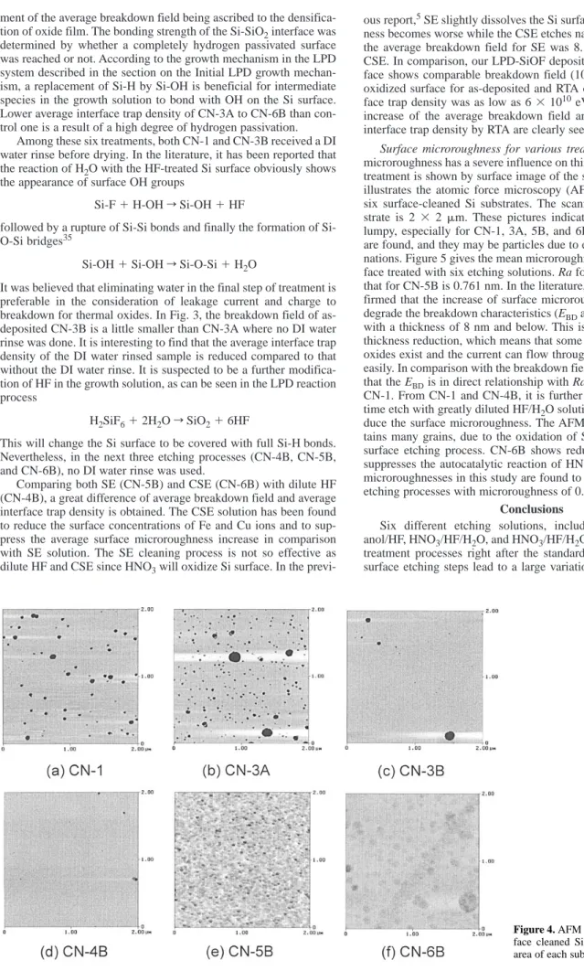
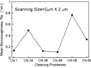
Surface microroughness for various treatments.—Since surface microroughness has a severe influence on thin oxide quality, the best treatment is shown by surface image of the six treatments. Figure 4 illustrates the atomic force microscopy (AFM) surface images for six surface-cleaned Si substrates. The scanning area of each sub- strate is 2 3 2 mm. These pictures indicate that the surfaces are lumpy, especially for CN-1, 3A, 5B, and 6B. Some black features are found, and they may be particles due to environmental contami- nations. Figure 5 gives the mean microroughness (Ra) for the Si sur- face treated with six etching solutions. Ra for CN-4B is 0.1 nm and that for CN-5B is 0.761 nm. In the literature,14,36,37it has been con- firmed that the increase of surface microroughness would severely degrade the breakdown characteristics (EBDand QBD) of a thin oxide with a thickness of 8 nm and below. This is due to effective oxide thickness reduction, which means that some areas of extremely thin oxides exist and the current can flow through these tunneling paths easily. In comparison with the breakdown field in Fig. 3, it is evident that the EBDis in direct relationship with Ra, with the exception of CN-1. From CN-1 and CN-4B, it is further concluded that a long- time etch with greatly diluted HF/H2O solution could effectively re- duce the surface microroughness. The AFM image of CN-5B con- tains many grains, due to the oxidation of Si by HNO3during the surface etching process. CN-6B shows reduced Ra because H2O2 suppresses the autocatalytic reaction of HNO3and Si. The surface microroughnesses in this study are found to be comparable to other etching processes with microroughness of 0.1-1 nm.14-18
Conclusions
Six different etching solutions, including dilute HF, meth- anol/HF, HNO3/HF/H2O, and HNO3/HF/H2O2, were used as surface treatment processes right after the standard RCA cleaning. These surface etching steps lead to a large variation of the degree of hy-
Figure 4. AFM surface images for six sur- face cleaned Si substrates. The scanning area of each substrate is 2 3 2 mm.
drogen passivation, which greatly affects the LPD-SiOF growing mechanism for the surface bonding process, and hence a prominent GDT is observed (<12 min). The breakdown distributions of RTA LPD-SiOF were found to be greatly improved (18% improvement) compared to as-deposited LPD-SiOF. This is believed due to densi- fication of the oxide network by driving out fluorine atoms. It is found that a two-step dilute HF (1:200 for HF/H2O) etching process can meet the requirements in ULSI fabrication in terms of high breakdown field (,10 MV/cm) and sufficiently low interface trap density (,1010eV21cm22). Furthermore, the RTA process can both improve the oxide quality and Si-SiO2interface characteristics (33%
reduction). Breakdown fields were demonstrated to be related to sur- face microroughness of various etching processes. A two-step etch- ing process shows the lowest microroughness of 0.1 nm.
Acknowledgments
This work was partially supported by the National Science Coun- cil of Republic of China under contract no. NSC 88-2736-L006-001.
National Cheng-Kung University assisted in meeting the publication costs of this article.
References
1. K. Lai, M. Y. Hao, W. H. Chen, and J. C. Lee, IEEE Electron Device Lett., EDL- 15, 446 (1994).
2. M. Chonko and V. Kaushik, The Physics and Chemistry of SiO2and the Si-SiO2 Interface 2, p. 267, Plenum Press, New York (1992).
3. R. Kroon, Jpn. J. Appl. Phys., 36, 5068 (1997).
4. R. K. Chanana and S. K. Srivastava, in IEEE International Conference on Plasma Science, p. 282, IEEE (1996).
5. M. Biavati, I. Perez-Quintana, A. Poggi, and E. Susi, J. Vac. Sci. Technol. B, 13, 2139 (1995).
6. G. Y. Pavlov, Mater. Res. Soc. Symp., 386, 321 (1995).
7. G. Vereecke, E. Rohr, and M. M. Heyns, in Diffusion and Defect Data Pt. B: Solid State Phenomena Proceedings of 1998 4th International Symposium on Ultra Clean Processing of Silicon Surfaces, p. 187 (1998).
8. J. Ruzyllo, E. Rohr, M. Baeyens, T. Bearda, P. Mertens, and M. Heyns, in Diffusion and Defect Data Pt. B: Solid State Phenomena Proceedings of 1998 4th Interna- tional Symposium Ultra Clean Processing of Silicon Surfaces, p. 85 (1998).
9. H. Park, D. Ko, P. Apte, C. R. Helms, and K. C. Saraswat, Electrochem. Solid-State Lett., 1, 77 (1998).
10. H. Habuka, T. Otsuka, and M. Katayama, J. Cryst. Growth, 186, 104 (1998).
11. R. Sugino, Y. Okui, M. Shigeno, S. Ohkubo, K. Takasaki, and T. Ito, J. Electro- chem. Soc., 144, 3984 (1997).
12. M. Alessandri, E. Bellandi, F. Pipia, F. Cazzaniga, K. Wolke, and M. Schenkl, in Diffusion and Defect Data Pt. B: Solid State Phenomena Proceedings of 1998 4th International Symposium on Ultra Clean Processing of Silicon Surfaces, p. 27 (1998).
13. T. Hattori, T. Osaka, A. Okamoto, K. Saga, and H. Kuniyasu, J. Electrochem. Soc., 145, 3278 (1997).
14. T. Ohmi, T. Tsuga, J. Takano, M. Kogure, K. Makihara, and T. Imaoka, IEICE Trans. Electrons, E75-C, 800 (1992).
15. R. Takizawa, T. Nakanishi, K. Honda, and A. Ohsawa, Jpn. J. Appl. Phys., 27, L2210 (1988).
16. T. H. Park, Y. S. Ko, T. E. Shim, J. G. Lee, and Y. K. Kim, J. Electrochem. Soc., 142, 571 (1995).
17. S. Verhaverbeke, M. Meuris, M. Schaekers, L. Haspeslagh, P. Mertens, M. M.
Heyns, R. De Blank, and A. Philipossian, in the Symposium of VLSI Digest of Tech- nical Papers, p. 22 (1992).
18. T. Shimono and M. Tsuji, IEICE Trans. Electrons, E75-C, 812 (1992).
19. C. F. Yeh, C. L. Chen, and G. H. Lin, J. Electrochem. Soc., 141, 3177 (1994).
20. K. Awazu, H. Kawazoe, and K. Seki, J. Non-Cryst. Solids, 151, 102 (1992).
21. J. S. Chou and S. C. Lee, J. Electrochem. Soc., 141, 3214 (1994).
22. C. F. Yeh and C. L. Chen, J. Electrochem. Soc., 142, 3579 (1995).
23. C. J. Huang, M. P. Houng, Y. H. Wang, and N. F. Wang, J. Vac. Sci. Technol. A, 16, 2646 (1998).
24. M. P. Houng, Y. H. Wang, N. F. Wang, W. J. Chang, and C. I. Hung, Mater. Chem.
Phys., 59, 39 (1999).
25. M. P. Houng, Y. H. Wang, N. F. Wang, C. J. Huang, and W. J. Chang, Jpn. J. Appl.
Phys., 36, L696 (1997).
26. W. S. Lu and J. G. Hwo, Appl. Phys. Lett., 66, 3322 (1995).
27. C. F. Yeh and S. L. Lin, J. Non-Crystal Solids, 187, 81 (1995).
28. W. S. Lu and J. G. Hwu, IEEE Electron Device Lett., EDL-17, 172 (1996).
29. M. P. Houng, C. J. Huang, Y. H. Wang, N. F. Wang, and W. J. Chang, J. Appl. Phys., 82, 5788 (1997).
30. A. Jakubowski and K. Iniewski, Phys. Status Solidi A, 89, 383 (1985).
31. L. Terman, Solid-State Electron., 5, 285 (1962).
32. T. Homma, T. Katoh, Y. Yamada, and Y. Murao, J. Electrochem. Soc., 140, 2410 (1993).
33. H. Nagayama, H. Honda, and H. Kawahara, J. Electrochem. Soc., 135, 2013 (1988).
34. M. M. Heyns, S. Verhaverbeke, M. Meuris, P. W. Mertens, H. Schmidt, M. Kubo- ta, A. Philipossian, K. Dillenbeck, D. Graf, A. Schnegg, and R. de Blank, Mater.
Res. Soc. Symp., 315, 35 (1993).
35. D. Graf, M. Grundner, and R. Schulz, J. Vac. Sci. Technol. A, 7, 808 (1989).
36. I. Oki, T. Biwa, J. Kudo, and H. Shibayama, IEICE Trans. Electrons, E75-C, 809 (1992).
37. T. Ohmi, M. Miyashita, M. Itano, T. Imaoka, and I. Kawanabe, IEEE Trans. Elec- tron Devices, ED-39, 537 (1992).
Figure 5. Mean surface microroughness (Ra) of the six etching processes.