行政院國家科學委員會補助專題研究計畫成果報告
以整齊排列之 DNA 分子進行奈米光刻
計畫類別:□ 個別型計畫 □ 整合型計畫 計畫編號:NSC 96-2221-E-006-129-
執行期間:96 年 08 月 01 日至 97 年 07 月 31 日
計畫主持人:莊怡哲 共同主持人:
計畫參與人員:張源炘、程俊傑、羅國峰
成果報告類型(依經費核定清單規定繳交):□精簡報告 □完整報告
本成果報告包括以下應繳交之附件:
□赴國外出差或研習心得報告一份
□赴大陸地區出差或研習心得報告一份
□出席國際學術會議心得報告及發表之論文各一份
□國際合作研究計畫國外研究報告書一份
處理方式:除產學合作研究計畫、提升產業技術及人才培育研究計畫 列管計畫及下列情形者外,得立即公開查詢
□涉及專利或其他智慧財產權,□一年□二年後可公開查詢 執行單位:國立成功大學化學工程學系
中 華 民 國 97 年 10 月 31 日
Aligned and Ordered DNA Molecules for Nanolithography Approaching Sub-nanometer Scale
Yuan-Hsin Chang (
張源炘), Jun-Jie Cheng(
程俊傑), Kuo-Feng Lo(
羅國峰)and Yi-Je Juang* (
莊怡哲) Department of Chemical Engineering
National Cheng Kung University
Abstract
One of the effective approaches to fabricate 1-D nanowires is the molecular combing/soft lithography technique, which can generate an aligned and ordered DNA nanostrands array [1].
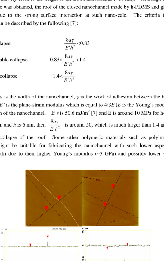
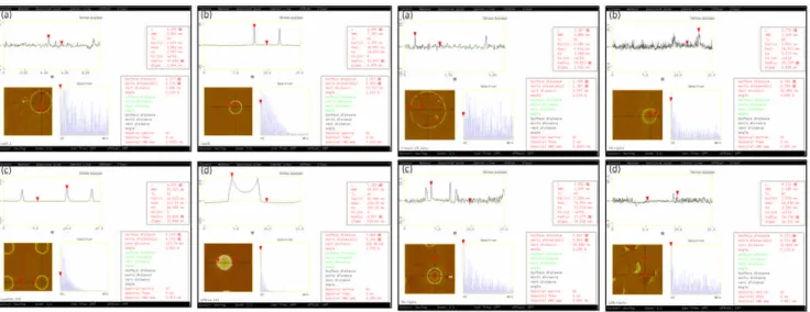
However, the technique and its potential for subsequent applications have not been fully investigated. In this study, different processing parameters such as center-to-center distance, applied pressure, peeling rate for PDMS mold and concentrations of DNA solutions were discussed. The DNA nanostrands array was then used as the template for metallization and fabrication of nanochannels. The results showed that proper applied pressure is required to generate the ordered DNA nanostrands. Moreover, shorter center-to-center distance, higher concentration of DNA solution and fast peeling rates for PDMS mold will facilitate fabricating long DNA nanostrands. A roller technique was proposed to provide better control over generating DNA nanostrands. As to metallization of DNA nanostrands, palladium nanowires and hybrid metallic nanowires (palladium and cobalt) on the modified glass substrate were obtained through electroless plating process. Proper activation time and reduction time in conjunction with surface modification of substrate is necessary to minimize the amount of metallic particles growing on the substrate. For fabrication of nanochannels, h-PDMS was used and nanochannels with deep around 6 nm were obtained. This provides a powerful alternative to fabricate long and aligned nanochannels for nanofluidic studies and applications. In addition, new micro/nanopatterning technique was also developed in this study.
Introduction
Nanofabrication has become one of the main streams when conducting advanced research and development in both academia and industries. Knowing the potentials of technology breakthrough and intense competition, researchers from all over the world have been devoting their efforts to this field with a strikingly fast pace. It is in consensus that nanofabrication is one key set of the methods for nanoscience and nanotechnology, bearing high expectations of leading to revolution in significant technologies and bringing tremendous impact to human life.
Applications of the nanofabrication techniques can be found in many areas ranging from
semiconductor industries and telecommunication to chemical/biological chips and detection.
The substrate materials used include silicon, metals, and polymers [2-4]. Several literatures reviewed variety of the nanofabrication techniques, which can be categorized into either top-down/bottom-up strategies or conventional/non-conventional methods [2, 5]. For example, scanning beam lithography, nanoimprint lithography, microcontact imprinting, scanning probe lithography, self-assembly, and so on. Among them, nanoimprint lithography (NIL) has been receiving great attention due to its promising capability of high throughput nanopatterning on large area and being a low-cost method [6]. For NIL to become one of the next generation lithographic techniques, mold making is one of the critical steps. There are several methods for fabricating molds with nanostructures such as electron beam lithography (EBL), dry etching, metal lift-off, etc.; however, either the fabrication process is too expensive, or the effective mold area is not large enough, or the smallest dimension of the features is larger than 50 nm. Recently, a modified molecular combing/soft lithography method was proposed to generate highly ordered DNA nanostrands, which were approximately 1.5 nm in height and can be up to 2 mm long [1]. This technique presents a great potential that it can be utilized not only to prepare for 1D nanostructures for electronic, magnetic, photonic, and chemical sensing applications but also for mold making with features at nano or approaching sub-nanometer scale. Although numerous applications and fabrication techniques can be built around this technique with DNA molecules as the template, further investigation has not been conducted.
Experimental 1. Materials
Polydimethyl siloxane (PDMS, Sylgard 184) was purchased from Dow Corning. -DNA was purchased from New England BioLabs. Tris-HCl (1M, pH=8), EDTA (0.5 M, pH=8), 2-mercaptoethanol, glycerol and bovine serum albumin (BSA) were purchased from Sigma.
Dimethylamine borane (DMAB) was purchased from Alfa Aesar. Palladium (II) acetate (>99.9 wt%) was purchased from UR-IPAL002 Corporation. Sodium citrate and cobalt chloride were purchased from J. T. Baker. 3-aminopropyltriethoxy silane (APTES) was purchased from Fluka. h-PDMS was purchased from Aldrich and Gelest.
2. Fabrication of DNA nanostrands
The PDMS stamp with an array of microwells was fabricated via soft lithographic process.
The diameter of the microwells is 5.5 m. A droplet of DNA solution was dispensed on the glass slide, followed by covering with the PDMS stamp. The stamp was then peeled off from the glass slide and the DNA nanostrands were generated, which were transferred onto another clean glass slide with or without surface modification by APTES.
3. Metallization of DNA nanostrands
A droplet of palladium acetate was dispensed on the glass slide with DNA nanostrands array for a period time in the dark (incubation or activated time). The glass slide was then blown dry, followed by dispensing a droplet of DMAB on the glass slide for a period of time (reduction time). After reduction, copious amount of DI water was used to rinse the glass slide and it was blown dry and stored in the Petri dish.
To fabricate Co/Pd nanowires, a droplet of solution containing cobalt chloride, DMAB and sodium citrate was dispensed on the glass slide with array of Pd nanowires which was placed on the hot plate set at 50
oC. After reaction, the glass slide was rinsed with copious amount of DI water, blown dry and stored in the Petri dish.
4. Fabrication of nanochannels
h-PDMS was spun on the glass slide with the DNA nanostrands, followed by curing inside the oven. A layer of PDMS was subsequently dispensed on top of the h-PDMS and cured at 65
oC for 2 hours. The whole assembly was peeled off from the glass slide afterwards.
5. Capillarity-assisted micro/nanopatterning
A droplet of bovine serum albumin (BSA) with different concentrations was dispensed on a glass substrate, followed by covering the PDMS stamp with array of microwells.
Fluorescein was added in the solution for visualization. After the solvent evaporated, the stamp was removed and the glass slide with patterns was examined using optical microscope and atomic force microscope (AFM).
Results and Discussion
1. Fabrication of DNA nanostrands
1.1 Effect of the applied pressure on the PDMS stamp
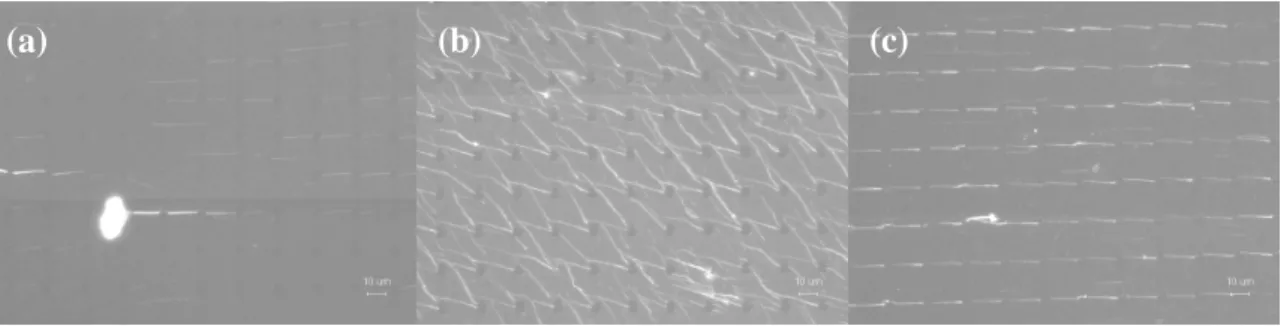
Figure 1 shows the generated DNA nanostrands under different applied pressure. If the applied pressure is too small, there are hardly DNA nanostrands generated on the stamp as shown in Figure 1(a), which might be due to lesser amount of the DNA solution inside the
Figure 1. The DNA nanostrands generated under different applied pressure: (a) 100, (b) 900, and (c) 460 g/cm
2.
(a) (b) (c)
microwells. On the other hand, if the pressure is too high, the zigzag-like network formation of the DNA nanostrands was observed as shown in Figure 1(b). This might be owing to the deformation of the PDMS stamp under high pressure, which leads to distortion of the microwells. The aligned and ordered DNA nanostrands array was generated under the proper applied pressure as shown in Figure 1(c).
1.2 Effect of the center-to-center (C-C) distance between microwells
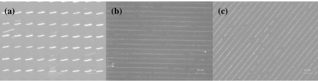
Figure 2 shows the DNA nanostrands generated using the PDMS stamps with different center-to-center distance between microwells. At the DNA concentration 50 g/ml, the long DNA nanostrands can be generated at a relatively large area with C-C equal to 10 m as shown in Figure 2(a). For C-C equal to 35 m, only short DNA nanostrands were observed (Figure 2(b)). As to 20 m, both long and short DNA nanostrands were generated (Figure 2(c)).
1.3 Effect of the DNA concentrations
Figure 3 shows the DNA nanostrands generated by using different DNA concentrations.
It can be seen that, when C-C equal to 11 m, the higher the DNA concentration, the more the long DNA nanostrands.
Figure 2. The DNA nanostrands generated using PDMS stamp with different C-C distances:
(a) 10, (b) 35, and (c) 20 m.
Figure 3. The DNA nanostrands generated with different DNA concentrations: (a) 20, (b) 50, and (c) 100 g/ml.
(a) (b) (c)
(a) (b) (c)
The relationship among the types of DNA nanostrands (short or long), DNA concentrations and C-C distance can be summarized in Table 1. In general, the shorter the C-C distance is and the higher the DNA concentration is, the easier the long DNA nanostrands can be generated.
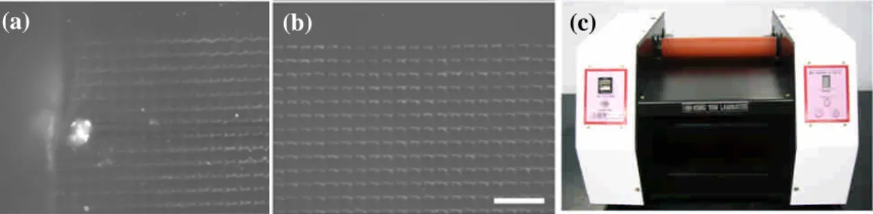
Since the technique was performed by manual operation, direction and uniformity of the DNA nanostrands on the PDMS stamp might not be well controlled, especially those near the corners and edge of the stamp. Figure 4(a) shows the DNA nanostrands generated near the edge of the PDMS stamp for some occasions by manual operation. By applying the roller technique, the direction of the DNA nanostrands was better controlled as shown in Figure 4(b). Although the prototype machine was constructed (Figure 4(c)), further modification is required to better control the roller gap, speed and so on.
2. Metallization of DNA nanostrands 2.1. Palladium (Pd) nanowires
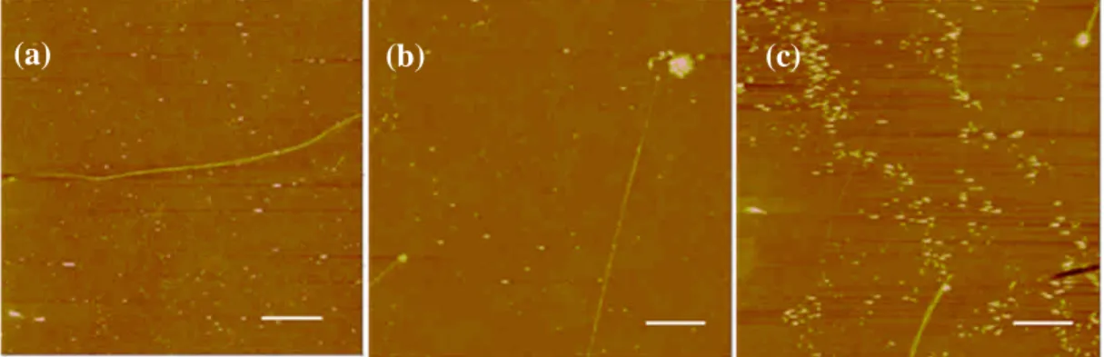
Figure 5 shows the Pd nanowires generated at different incubation times, followed by 30-second reduction time, on the glass slide. It can be seen that there are many Pd nanoparticles on the surface of the glass slide, which leads to the high background noise. In order to minimize the background noise, the glass slide was modified with APTES, followed by metallization process. The background noise was substantially reduced for the short incubation times as shown in Figure 6. As to the long incubation time, many Pd
DNA concentration(μg/ml)
Center to Center distance(μm)
20 50 100 200
11 △ ○ ○ ○
15 △ △ ○ ○
20 △ △ ○ ○
35 △ △ △ ○
DNA concentration(μg/ml)
Center to Center distance(μm)
20 50 100 200
11 △ ○ ○ ○
15 △ △ ○ ○
20 △ △ ○ ○
35 △ △ △ ○