Optical properties of well-aligned multiwalled carbon nanotube bundles
M. F. Lin
Department of Physics, National Cheng Kung University, Tainan, Taiwan 701, The Republic of China F. L. Shyu
Department of Electronics Engineering, Fortune Institute of Technology, Kaohsiung, Taiwan 842, The Republic of China R. B. Chen
Department of Physics, Yung Ta Institute of Technology & Commerence, Pingtung, Taiwan 909, The Republic of China 共Received 23 September 1999兲
The optical properties of well-aligned multiwalled carbon nanotube bundles are studied within the gradient approximation. The imaginary共real兲 part of the transverse dielectric function exhibits a special peak 共dip兲 at frequency ⬃2␥0 共␥0 is the nearest-neighbor overlap integral兲. Consequently the loss function shows a prominent-plasmon peak at ⬎2␥0. The plasmon also induces a strong and abrupt edge in the reflectance spectrum. These features are similar to those of graphite. The optical properties are hardly affected by the chiral angle of carbon nanotube; moreover, they are insensitive to small variation in the radius of carbon nanotube. On the other hand, the optical properties strongly depend on the polarization direction of an external electric field. The well-aligned multiwalled carbon nanotubes with high radius uniformity, which were recently reported by Fan et al.关Science 283, 512 共1999兲兴, could be used to verify the predicted optical properties.
Carbon nanotubes have attracted a lot of interest since their discovery by Iijima1in 1991. A carbon nanotube con- sists either of a single tubule or of several coaxial tubules with a nanoscaled radius r⬃3.4– 150 Å. Carbon atoms are arranged on a cylindrical nanotube in a chiral or a chiral fashion. A single-walled carbon nanotube is a semiconductor or a metal, which depends the radius and the chiral angle.2–4 When carbon nanotubes are closely packed together, a three- dimensional共3D兲 carbon nanotube bundle is formed. Carbon nanotube bundles made up of single-walled5,6or multiwalled nanotubes7–9 had been fabricated. The alignment of carbon nanotubes and their size distribution are very important for both fundamental studies and device applications. The single-walled carbon nanotubes in a bundle might bend along the tubular axis.5,6 To improve the straightness, the well-aligned mutliwalled carbon nanotube bundles were first made by de Heer et al.7The distribution of the multiwalled nanotube radius (r⬃5⫾2.5 nm) was too broad. Only re- cently, it is possible to largely produce multiwalled carbon nanotube bundles with a narrow radius distribution (r⬃8
⫾1 nm).9These systems enable us to study some essential physical properties of carbon nanotube bundles, say, optical properties. In this work, we study the optical properties of well-aligned multiwalled carbon nanotube bundles, including the transverse dielectric function 共⑀兲, the loss function, and the reflectance共R兲. Their dependence on the polarization di- rection of an external electric field, the chiral angle of carbon nanotube共兲, and the radius of carbon nanotube 共r兲 is inves- tigated. We will also compare these properties between mul- tiwalled carbon nanotube bundles and graphite.10
There have been some reports on optical properties of carbon nanotubes, both experimentally and theoretically. The optical ellipsometry was used to directly measure the trans- verse dielectric function of a multiwalled carbon nanotube
bundle.7 The dielectric function was found to show only a special peak or dip, owing to the superposition of the contri- butions from the coaxial nanotubes 共to be discussed later兲.
Theoretical studies are mainly focused on the optical prop- erties of single-walled carbon nanotube bundles.11–14 A single-walled carbon nanotube has cylindrical symmetry.
Therefore, the magneto-optical absorption spectra exhibit the Aharonov-Bohm quantum oscillation.11 There are a lot of special structures in the transverse dielectric function,11–14 since a single-walled carbon nanotube has many 1D sub- bands. Moreover, the -electronic collective excitations 共 plasmons兲 lead to a prominent peak in the loss function and a weak edge structure in the reflectance spectrum.12
We use the tight-binding model to calculate the band and the gradient approximation to evaluate the transverse dielectric function. Since carbon nanotubes are highly aniso- tropic, their optical properties are expected to strongly de- pend on the polarization direction of an external electric field. In this work, we consider the effects of changes in both the chiral angle of carbon nanotube and the multiwalled nanotube radius. It is important to clarify whether the distri- bution of multiwalled carbon nanotubes9would significantly affect optical properties. Our study shows that there is a spe- cial dip 共peak兲 structure in the real 共imaginary兲 part of the transverse dielectric function at⬃2␥0 共␥0⯝2.4– 3.0 eV is the nearest-neighbor overlap integral2,4兲. The loss function exhibits a pronounced -plasmon peak at⬎2␥0. Further- more, theplasmon induces a strong and abrupt edge in the reflectance spectrum. The calculated results are consistent with the ellipsometry experiments.7
The geometric structure of a single-walled carbon nano- tube is uniquely determined by the chiral vector Rx⫽ma1
⫹na2, which connects two crystallographically equivalent PRB 61
0163-1829/2000/61共20兲/14114共5兲/$15.00 14 114 ©2000 The American Physical Society
sites on a 2D graphite sheet.4The chiral angle and the radius of a 共m, n兲 nanotube are, respectively, ⫽tan⫺1关⫺)n/(2m
⫹n)兴 and
r⫽兩Rx兩 2 ⫽
b冑3共m2⫹mn⫹n2兲
2 共b⫽1.42 Å兲.
The band is calculated with the tight-binding model like that employed for a graphite sheet.15The energy dispersions and the corresponding wave functions are denoted by Ec,v(kx,ky) and⌿c,v(kx,ky), respectively.16The superscript c (v) represents an unoccupied antibonding*band共occu- pied bonding band兲. The transverse wave vector kx is equal to J/r, where J is the quantized angular momentum adopted as a subband index. The axial wave vector ky is confined to the first Brillouin zone共BZ兲. There are two types of electronic structures according to geometric structures.
Type-I carbon nanotubes, which correspond to 2m⫹n⫽3i 共i an integer兲, are semiconductors with energy gap Eg
⫽␥0b/r. Others are metallic type-II carbon nanotubes with Eg⫽0.
We consider a uniform carbon nanotube bundle in which the same multiwalled nanotubes are arranged in a triangular lattice5with the intertube distance d(⫽3.4 Å).1At zero tem- perature, the inter--band excitations from the occupied
-band states to the unoccupied*-band states are the only excitation channel. Within the relaxation-time approximation,17 the transverse dielectric function including all contributions of inter--band excitations is given by
⑀共兲⫽⑀0⫺ 16e2 )共2r⫹d兲2 兺
kx,kx⬘,i 冕1st BZ
dky 2
⫻
冟 冓⌿ic共kx⬘,ky兲冏
Eˆm•Pe冏
⌿iv共kx,ky兲冔 冟
2
vc,i
2 共kx,kx⬘,ky兲
⫻
再
⫺vc,i共kx1,kx⬘,ky兲⫹i⌫⫺ 1
⫹vc,i共kx,kx⬘,ky兲⫹i⌫
冎
, 共1兲wherevc,i(kx,kx⬘,ky)⫽Ei
c(kx⬘,ky)⫺Ei
v(kx,ky) is the inter-
-band excitation energy. The subscript i represents the ith nanotube among the N-shell coaxial nanotubes, ⑀0 is the background dielectric constant, and ⌫ is the energy width due to various deexcitation mechanisms. The velocity matrix element 具⌿i
c(kx⬘,ky)兩Eˆ•P/me兩⌿i
v(kx,ky)典 is evaluated within the gradient approximation.17,12 The weak intertube interactions are neglected in Eq. 共1兲. They only affect the low-energy elecronic structure for E⬍0.1 eV.18,19The inde- pendent nanotube approximation should be a reasonable model for⬎0.1 eV.
The calculations are principally based on the following parameters:⑀0⫽2.4 and ⌫⫽0.033␥0共Refs. 12 and 13兲 关⌫ is 0.1 eV for ␥0⫽3.033 eV 共Ref. 4兲兴. We construct a multi- walled carbon nanotube9with outer radius ro⫽80 Å and in-
ner radius ri⫽25.5 Å. The total shell number N is 17. A single-walled nanotube of a fixed radius may have different chiral angles and therefore may have different electronic structures. In this work, we randomly choose nine type-I nanotubes and eight type-II nanotubes. It will be demon- strated that optical properties are not affected by different chiral angles 共or the detailed electronic structure of each component nanotube兲.
The dielectric functions ⑀储 and ⑀⬜, which, respectively, correspond to the parallel (E储储yˆ) and the perpendicular (E⬜) polarizations, are evaluated explicitly in this study. We first examine the dielectric function for E储. The selection rule is
⌬ky⫽0 and ⌬J⫽L⫽0 关Eq. 共1兲兴. The angular momentum transfer L vanishes. Consequently, only the vertical inter-- band transitions from theto the*subbands of the same J’s are allowed. The dielectric function⑀储, as shown in Fig.
1 by the solid curves, reveals two main characteristics. Only very weak ripples exist in ⑀储 for ⬍2␥0, i.e., ⑀储 is almost featureless in this frequency range. The imaginary共real兲 part of the dielectric function ⑀2
储 (⑀1
储) exhibits a prominent peak 共dip兲 structure near ⫽2␥0 共at a frequency slightly greater than 2␥0兲. These two characteristics could also be found in graphite10共to be discussed later兲.
For the E⬜ case, the selection rule is ⌬ky⫽0 and ⌬J
⫽L⫽⫾1. These rules can be easily identified from Eˆ•P
⬀sin␣P␣⫽(ei␣⫺e⫺i␣)P␣/2i 关in Eq. 共1兲兴, where␣ is the azi- muthal angle. Electrons in the occupied subband of J are excited to the unoccupied * subband of J⫾1. The main features in ⑀⬜ 共the dashed curves in Fig. 1兲 are similar to those in ⑀储. Both⑀⬜ and⑀储 exhibit no special feature for
⬍2␥0 and have similar characteristic structures at
⬃2␥0. However, there are two important differences be- FIG. 1. The real (⑀1) and the imaginary (⑀2) parts of the trans- verse dielectric functions are shown for a multiwalled carbon nano- tube bundle with shell number N⫽17 at energy width ⌫
⫽0.033␥0. The solid and the dashed curves correspond to the par- allel and the perpendicular polarization directions, respectively. The unit of frequency is 2␥0.
tween ⑀⬜ and⑀储. The minimum excitation energy is Eic(J
⫹1,ky)⫺Eiv(J,ky) for E⬜, so there exists a special peak in
⑀⬜2 at small(⬃0.056␥0). The optical transition probability for E⬜ is about half of that for E储. Consequently, ⑀⬜2 is smaller than⑀2
储 at all’s and⑀⬜1 is smaller 共larger兲 than⑀1
储
for ⬍2␥0 (⬎2␥0). At ⬃2␥0, the special structure in
⑀⬜ is less obvious. This important difference clearly illus- trates the strong anisotropy of optical properties. Moreover, it would render the optical spectra for the case of E⬜ rela- tively weak, e.g., a weaker-plasmon peak in the loss func- tion 共Fig. 2兲.
The facts that the transverse dielectric function exhibits the special structure at⬃2␥0 and the featureless behavior at ⬍2␥0 deserve a closer investigation. Within the tight- binding model,4,16the -electronic states of a single-walled carbon nanotube are derived from those of a graphite sheet.
For the hexagonal Brillouin zone of a graphite sheet,15 the middle point M between the K and K⬘ corners is a saddle point in the energy-wave-vector space. At this k point, the inter--band excitation energy is 2␥0. Each carbon nano- tube of the multiple shells must sample some of its eigen- states near the M point. As a result of the flat band structure, such states would lead to a special structure in ⑀ at
⬃2␥0. We may understand the featureless spectra for
⬍2␥0 as follows. Each carbon nanotube has many 1D sub- bands because of the transverse periodical boundary condi- tion. For example, the number of subbands is more than 70 for a carbon nanotube with r⬎20 Å. Because of to these 1D subbands, a single-walled carbon nanotube bundle11–14 ex- hibits many peak structures for ⬍2␥0 in addition to the special structure at⬃2␥0. However, for a multiwalled car- bon nanotube bundle, the superposition of the coaxial nano- tubes would make peaks disappear except the common struc- ture at ⬃2␥0. In other words, the mixing effect of the coaxial nanotubes is the cause for the featureless behavior of
⑀ at⬍2␥0. In addition, the similarity in the -electronic
structures could explain why multiwalled carbon nanotube bundles and graphite10exhibit similar dielectric functions.
Three main features of the transverse dielectric functions are consistent with the ellipsometry experiments.7 They in- clude a featureless behavior for ⬍2␥0, a special peak or dip at⬃2␥0, and a relatively strong peak or dip in the E储 case. Also notice that ⑀储 and ⑀⬜ had been calculated for a single-walled carbon nanotube bundle 共Fig. 4 in Ref. 13兲. A very large energy width (⌫⫽0.2␥0) is required to explain the experimental result,7 the featureless behavior of ⑀ at
⬍2␥0. The reason for the featureless behavior, as we have pointed out above, should be the superposition of the coaxial carbon nanotubes, instead of a very large ⌫.
The transverse dielectric function is used to calculate the loss function Im关⫺1/⑀兴 at zero momentum transfer. The dip structure in the real part of the dielectric function leads to a pronounced peak in the loss function, as shown in Fig. 2.
This peak is attributed to the collective excitations ofelec- trons. The plasmons for E储 共solid curve兲 and for E⬜ 共dashed curve兲 come from the superposition of L⫽0 and L
⫽1 collective excitations of all carbon nanotubes, respec- tively. The latter has a weaker plasmon peak and a lower plasmon frequency, since the optical excitations are less ef- ficient in the E⬜ case. The plasmon also exists in graphite.10 Compared with a multiwalled carbon nanotube bundle, graphite exhibits a stronger plasmon peak and a higher -plasmon frequency. That graphite has a higher
-electron density could explain the differences for the plasmon.
The plasmons at the long-wavelength limit could be measured by the electron-energy-loss spectroscopy 共EELS兲.
There are some experimental measurements on a multiwalled carbon nanotube20–23as well as a carbon nanotube film.24,25 The plasmons are identified from the pronounced peak in the loss spectrum. Using EELS to investigate theplasmons in a multiwalled carbon nanotube bundle, one needs to specify the direction of the momentum transfer for the prob- ing electrons. For E储 (E⬜), the momentum transfer is parallel 共perpendicular兲 to the nanotube axis. The momentum trans- fer for both cases is negligible. In addition to the EELS, the optical spectroscopy could also be used to measure the plasmons. In an experiment, the reflectance spectrum is first measured, then the dielectric function and the loss function are determined by using the Kramers-Kronig relations.10
The reflectance is calculated from the relation R()⫽兩1
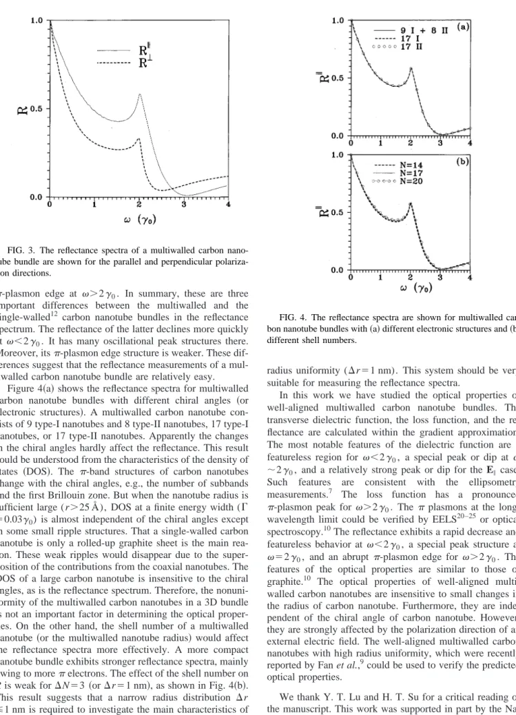
⫺冑⑀()兩2/兩1⫹冑⑀()兩2. The spectrum, as shown in Fig. 3, decreases quickly as increases from zero. R is essentially featureless for ⬍2␥0. When frequency approaches 2␥0, reflectance begins to increase. R rises to a local maximum at
⫽2␥0 and then rapidly drops to a minimum. The abrupt edge in reflectance spectrum is caused by the plasmon.
Also, note that the characteristic peak near the plasmon edge is absent in the spectrum of an ordinary metal.26The reflec- tance spectrum is significantly affected by the polarization directions. Compared to R⬜, R储 exhibits a relatively pro- nounced -plasmon edge structure. The main reason is that the optical response is stronger for the E储 case.
The frequency-dependent characteristics of the reflectance spectrum are similar to those of graphite.10 The similarities include a rapid decrease and featureless behavior at
⬍2␥0, a special peak structure at ⫽2␥0, and an abrupt FIG. 2. The loss functions of a multiwalled carbon nanotube
bundle are shown for the parallel and perpendicular polarization directions.
-plasmon edge at ⬎2␥0. In summary, these are three important differences between the multiwalled and the single-walled12 carbon nanotube bundles in the reflectance spectrum. The reflectance of the latter declines more quickly at ⬍2␥0. It has many oscillational peak structures there.
Moreover, its-plasmon edge structure is weaker. These dif- ferences suggest that the reflectance measurements of a mul- tiwalled carbon nanotube bundle are relatively easy.
Figure 4共a兲 shows the reflectance spectra for multiwalled carbon nanotube bundles with different chiral angles 共or electronic structures兲. A multiwalled carbon nanotube con- sists of 9 type-I nanotubes and 8 type-II nanotubes, 17 type-I nanotubes, or 17 type-II nanotubes. Apparently the changes in the chiral angles hardly affect the reflectance. This result could be understood from the characteristics of the density of states 共DOS兲. The -band structures of carbon nanotubes change with the chiral angles, e.g., the number of subbands and the first Brillouin zone. But when the nanotube radius is sufficient large (r⬎25 Å), DOS at a finite energy width (⌫
⫽0.03␥0) is almost independent of the chiral angles except in some small ripple structures. That a single-walled carbon nanotube is only a rolled-up graphite sheet is the main rea- son. These weak ripples would disappear due to the super- position of the contributions from the coaxial nanotubes. The DOS of a large carbon nanotube is insensitive to the chiral angles, as is the reflectance spectrum. Therefore, the nonuni- formity of the multiwalled carbon nanotubes in a 3D bundle is not an important factor in determining the optical proper- ties. On the other hand, the shell number of a multiwalled nanotube 共or the multiwalled nanotube radius兲 would affect the reflectance spectra more effectively. A more compact nanotube bundle exhibits stronger reflectance spectra, mainly owing to moreelectrons. The effect of the shell number on R is weak for⌬N⫽3 共or ⌬r⫽1 nm兲, as shown in Fig. 4共b兲.
This result suggests that a narrow radius distribution ⌬r
⭐1 nm is required to investigate the main characteristics of the optical properties. Fan et al.9had successfully made the well-aligned multiwalled carbon nanotube bundle with high
radius uniformity (⌬r⫽1 nm). This system should be very suitable for measuring the reflectance spectra.
In this work we have studied the optical properties of well-aligned multiwalled carbon nanotube bundles. The transverse dielectric function, the loss function, and the re- flectance are calculated within the gradient approximation.
The most notable features of the dielectric function are a featureless region for ⬍2␥0, a special peak or dip at
⬃2␥0, and a relatively strong peak or dip for the E储 case.
Such features are consistent with the ellipsometry measurements.7 The loss function has a pronounced
-plasmon peak for ⬎2␥0. The plasmons at the long- wavelength limit could be verified by EELS20–25 or optical spectroscopy.10The reflectance exhibits a rapid decrease and featureless behavior at ⬍2␥0, a special peak structure at
⫽2␥0, and an abrupt -plasmon edge for ⬎2␥0. The features of the optical properties are similar to those of graphite.10 The optical properties of well-aligned multi- walled carbon nanotubes are insensitive to small changes in the radius of carbon nanotube. Furthermore, they are inde- pendent of the chiral angle of carbon nanotube. However, they are strongly affected by the polarization direction of an external electric field. The well-aligned multiwalled carbon nanotubes with high radius uniformity, which were recently reported by Fan et al.,9could be used to verify the predicted optical properties.
We thank Y. T. Lu and H. T. Su for a critical reading of the manuscript. This work was supported in part by the Na- tional Science Council of Taiwan, and the Republic of China under Grant No. NSC 89-2112-M-006-011.
FIG. 4. The reflectance spectra are shown for multiwalled car- bon nanotube bundles with共a兲 different electronic structures and 共b兲 different shell numbers.
FIG. 3. The reflectance spectra of a multiwalled carbon nano- tube bundle are shown for the parallel and perpendicular polariza- tion directions.
1S. Iijima, Nature共London兲 354, 56 共1991兲.
2J. W. Mintwire, B. I. Dunlap, and C. T. White, Phys. Rev. Lett.
68, 631共1992兲.
3N. Hamada, S. I. Sawada, and A. Oshiyama, Phys. Rev. Lett. 68, 1579共1992兲.
4R. Saito, M. Fujita, G. Dresselhaus, and M. S. Dresselhaus, Appl.
Phys. Lett. 60, 2204共1992兲; Phys. Rev. B 46, 1804 共1992兲.
5A. Thess et al., Science 273, 483共1996兲.
6S. Bandow, S. Asaka, Y. Saito, A. M. Rao, L. Grigorian, E.
Richter, and P. C. Eklund, Phys. Rev. Lett. 80, 3779共1998兲.
7W. A. de Heer, W. S. Bacsa, A. Chalelain, T. Gerifin, R.
Humphrey-Baker, L. Forro, and D. Vargte, Science 268, 845 共1995兲.
8Z. F. Ren, Z. P. Huang, J. W. Xu, J. H. Wang, P. Buch, M. P.
Siegal, and P. N. Provencio, Science 282, 1105共1998兲.
9S. Fan, M. G. Chapline, N. R. Franklin, T. W. Tombler, A. M.
Cassell, and H. Dai, Science 283, 512共1999兲.
10E. A. Taft and H. R. Philipp, Phys. Rev. 138, A197共1965兲.
11H. Ajiki and T. Ando, Physica B 201, 349共1994兲.
12M. F. Lin and K. W.-K. Shung, Phys. Rev. B 50, 17 744共1994兲.
13S. Tasaki, K. Maekawa, and T. Yamabe, Phys. Rev. B 57, 9301 共1998兲.
14J. W. Mintwire and C. T. White, Synth. Met. 77, 231共1996兲.
15P. R. Wallace, Phys. Rev. 71, 622共1947兲.
16For the details of the electronic structure see M. F. Lin and D. S.
Chuu, Phys. Rev. B 56, 4996共1997兲.
17L. G. Johnson and G. Dresselhaus, Phys. Rev. B 7, 2275共1973兲.
18R. Saito, G. Dresselhaus, and M. S. Dresselhaus, J. Appl. Phys.
73, 494共1993兲.
19Y. K. Kwon and D. Tomanek, Phys. Rev. B 58, 16 001共1998兲.
20R. Kuzuo, M. Terauchi, and M. Tanaka, J. Phys. Soc. Jpn. 31, L1484共1992兲.
21P. M. Ajayan, S. Iijima, and T. Ichihashi, Phys. Rev. B 47, 6859 共1993兲.
22V. P. Dravid, X. W. Lin, Y. Wang, X. K. Wang, A. Yee, J. B.
Ketterson, and R. P. H. Chang, Science 259, 1601共1993兲.
23L. A. Bursill, P. A. Stadelmann, J. L. Peng, and S. Prawer, Phys.
Rev. B 49, 2882共1994兲.
24R. Kuzuo, M. Terauchi, M. Tanaka, and Y. Saito, Jpn. J. Appl.
Phys., Part 2 33, L1316共1994兲.
25T. Pichler, M. Knupfer, M. S. Golden, J. Fink, A. Rinzler, and R.
E. Smalley, Phys. Rev. Lett. 80, 4729共1998兲.
26J. M. Ziman, Principles of the Theory of Solids共Cambridge Uni- versity Press, Cambridge, 1972兲.