Evidence of the ultrahigh dielectric constant of CaSiO3-doped CaCu3Ti4O12 from its dielectric response, impedance spectroscopy, and microstructure
Tsang-Tse Fang,*Wei-Jie Lin, and Chia-Ying Lin
Department of Materials Science and Engineering, National Cheng Kung University, Tainan, Taiwan 70101, Republic of China 共Received 14 December 2006; revised manuscript received 9 February 2007; published 24 July 2007兲
The temperature and frequency dependences of the dielectric responses and the complex impedance spectra of polycrystalline CaCu3Ti4O12共CCTO兲 doped with CaSiO3have been investigated. The dielectric responses show two Maxwell-Wagner-type relaxations including insulating layers of grain boundaries and domain bound- aries and semiconducting grains. The behavior of the temperature dependence of the dielectric constant at 1 kHz is demonstrated to be determined by the frequency dependence of the dielectric constant of two super- posed dielectric relaxations at different temperatures. In contrast to the undoped CCTO, an extra semicircle clearly appears in the complex impedance plots of CaSiO3-doped CCTO. The results further confirm the presence of the domain boundaries, and their resistivity is lower than that of the grain boundaries. The microstructures have been characterized and the compositions of the grains, grain boundaries, and the second phases have been determined quantitatively. The Si ions are proved to be segregated to the grain boundaries.
The grain-boundary phases consist of a main Si-rich amorphous phase and a small amount of nanosized Cu-rich particles. The Cu-rich particles are present at grain edges or corners of the microstructures. The variations of the electrical conduction and the dielectric responses are related to the reduction of the concen- tration of the excess Cu ions along the grain boundaries.
DOI:10.1103/PhysRevB.76.045115 PACS number共s兲: 77.22.Ch, 77.22.Gm, 77.84.Dy
I. INTRODUCTION
CaCu3Ti4O12 共CCTO兲 has recently drawn a lot of atten- tion due to the fact that it possesses a very high dielectric constant of about 104– 105at radio frequency and below near room temperature, and it also shows a good temperature sta- bility over a wide temperature range from 100 to 600 K.1–3 Both properties are significant for the device implementa- tion. However, such a high dielectric constant is not related to the intrinsic nature of the polarization4,5 or ferroelectricity.1,2 It has further been suggested to be an ex- trinsic effect contributed from the interface.1–3,6–8 Several models1,8–15 have been proposed to explain the unusual di- electric responses of both polycrystalline and single-crystal CCTO. However, the fundamental problems regarding the composition-property relationships remain unresolved. Nev- ertheless, the recent report16 has indicated that the Cu defi- ciency may be the origin for inducing the high dielectric constant of CCTO.
There exist very few reports related to the impurity effect on CCTO,17–19 in which some transition metal ions are shown to have conspicuous effects. Therefore, further pursu- ing the impurity effect would be helpful to explore the rea- sons for the development of the ultrahigh dielectric constant of CCTO. With the knowledge that the Zr ions have a sig- nificant influence on the behavior of the temperature depen- dence of the dielectric responses of BaTiO3,20 the effect of the Zr ions on CCTO has been studied.21 It was found that the dielectric constant of CCTO doped with ZrSiO4 was 1 order of magnitude higher than those of undoped as well as ZrO2-doped CCTO.21Moreover, significant variations in the dielectric properties, electrical conduction, and their micro- structures were observed when CCTO was doped with these two dopants.21 Recent report22 showed that the addition of ZrO2 actually lowered the dielectric constant of CCTO,
which indicates that Si instead of Zr ions play an important role in enhancing the dielectric constant of ZrSiO4-doped CCTO. This fact stimulates us to pursue the study of the influence of Si ions on the properties of CCTO.
In the present work, we clarify the role of the Si ions in the microstructure change, the electrical conduction, and the dielectric responses of CaSiO3-doped CCTO. Detailed analy- ses of microstructure, composition, and complex impedance spectra are carried out to support the suggestions about the microstructure-composition-property relationships.
II. EXPERIMENT
Appropriate amounts of high purity CaCO3 共99.95%兲, CuO 共99.7%兲, TiO2 共99.9%兲, and CaSiO3 共99.5%兲 reagents were used to prepare undoped and CaSiO3-doped CCTO. In CaSiO3-doped CCTO, only the results of 2 mol % of CaSiO3 are presented here. CaSiO3 was selected instead of SiO2as the dopant due to the fact that the former is more reactive and easier to dissolve as Si ions in CCTO at low tempera- tures共⬍1100 °C兲. In a typical preparation condition, the ap- propriate amounts of powders were mixed in a ball mill with ZrO2 balls for 12 h. After drying, the powder was calcined for 2 h at 950 ° C in air. Then, it was milled again for 12 h.
The pellets were prepared by pressing the calcined powders in the 11 mm diameter steel die. The prepared pellets were sintered at 1065 ° C in air for 20 h and then furnace cooled to room temperature. Sintered pellets were cut, polished, and thermally etched for microstructural observation. High reso- lution analytical electron microscope 共HRAEM兲 and scan- ning electron microscope 共SEM兲 equipped with energy- dispersive x-ray spectrum 共EDS兲 were used to analyze microstructures and compositions. Two-probe method was used for the measurement of direct-current共dc兲 resistivity at room temperature. The impedance measurements were taken
with an applied voltage of 100 mV using a Hewlett-Packard 4284 A precision LCR meter over the frequency range 20 Hz– 1 MHz at selected temperatures between −90 and 150 ° C. In-Ga electrode was used for the electrical conduc- tion and impedance measurements.
III. RESULTS AND DISCUSSION
In Fig.1, we present the frequency dependence of the real part共⬘兲 and the imaginary part 共⬙兲 of the complex dielec- tric constant of CaSiO3-doped CCTO at different tempera- tures. The spectra of⬘versus frequency shown in Fig.1共a兲 reveal a complicated manner. They basically include two Maxwell-Wagner-type relaxations23with different relaxation times, and each contains a response with two frequency- independent plateaus共indicating the static and optical dielec- tric constants兲23 separated by a dispersion. The spectra shown in Fig. 1共a兲 essentially are a superposition of these
two dielectric relaxations at different temperatures. The pla- teau with higher dielectric constant is the sum of the static dielectric constants of both dielectric relaxations. It decreases with increasing temperature when the temperatures are above room temperature. The plateau with lower dielectric constant is only contributed by the static dielectric constant of the dielectric relaxation with smaller relaxation time. Moreover, the spectra of these two dielectric relaxations are displaced to higher frequencies with increasing measuring temperature.
This phenomenon was also reported for the undoped CCTO at high measuring temperatures.24 The spectra of ⬙ versus frequency shown in Figs. 1共b兲–1共d兲 reveal two Debye-like relaxation peaks at high and low frequencies. These two peaks shift to higher frequencies and their height decreases as the temperature increases. The relaxation time 共兲 of the frequency dependence of the dielectric constant can be ob- tained from the peaks shown in Figs. 1共b兲–1共d兲. However, the low-frequency peak is out of the range, and its value FIG. 1. Frequency dependence of the complex dielectric constant of CaSiO3-doped CCTO at different temperatures:共a兲 real part 共⬘兲 共the dash line at 1 kHz is to reveal the⬘ values at different temperatures兲 and 关共b兲–共d兲兴 imaginary part 共⬙兲 showing the high-frequency Debye-like peaks in共b兲 and 共c兲 but out of range in 共d兲.
cannot be evaluated. Using the Arrhenius law, =0e共E/kT兲 共where0 is the prefactor, Edenotes the activation energy for the response, k is the Boltzmann constant, and T is abso- lute temperature兲. The Evalue of the high-frequency peaks is determined from Fig.2of lnversus 1 / T. The obtained E value of 0.12 eV agrees well with the reported values for grain conductivity in CCTO.14,24
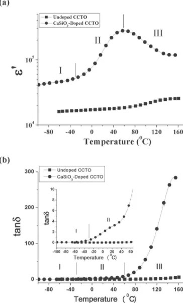
In Fig.3, we compared the temperature dependence of the dielectric properties of the undoped and CaSiO3-doped CCTO at 1 kHz. It can be observed in Fig. 3共a兲 that the dielectric constants of CCTO doped with CaSiO3 show strong temperature dependence, and the magnitude increases rapidly to a maximum and then declines. This temperature- dependent dielectric behavior usually occurs in low- resistivity CCTO, arising from either the processing14 or high-temperature measurement.24,25 Although it has been suggested to be a relaxor behavior,25it is found out not to be true by the following analyses. The spectrum of the CaSiO3-doped CCTO shown in Fig. 3共a兲 can essentially be divided into three regions. Region I 共for temperature
⬍−30 °C represents the gradual increase of the dielectric constant. Region II 共in the temperature range from
−30 to 60 ° C兲 represents the rapid increase of the dielectric constant. Region III 共for temperatures ⬎60 °C兲 represents the decrease of the dielectric constant. These three regions can further be rationalized by the values of the dielectric constant at 1 kHz共indicated by a dash line兲 in Fig.1共a兲. The dielectric constants in region I are determined by the plateau with lower dielectric constant in Fig.1共a兲共see the intercepts at −50 and −30 ° C兲. The dielectric constants in region II are determined by the dispersion region between these two pla- teaus in Fig.1共a兲共see the intercepts at 0, 30, and 50 °C兲. The dielectric constants in region III are determined by the pla- teau with higher dielectric constant in Fig.1共a兲共see the in- tercepts at 100 and 150 ° C兲. Accordingly, the temperature- dependent dielectric behavior of the CaSiO3-doped CCTO measured at a fixed frequency basically results from the fre- quency dependence of the dielectric constant of two super- posed dielectric relaxations at different temperatures. Figure 3共b兲 shows the temperature dependence of the dissipation factor 共tan␦兲 of undoped and CaSiO3-doped CCTO. It is interesting to note that for CaSiO3-doped CCTO, it can also be divided into three regions, which are equivalent to those
of the temperature-dependent dielectric constant关Fig.3共a兲兴.
The dissipation factor remains constant in region I, increases rapidly in region II, and increases much more sharply in region III. Moreover, there is a discernable bump in region II 关see the inset in Fig.3共b兲兴.
In order to understand the responses of the two dielectric relaxations shown in Fig.1, the complex impedance analyses have been performed. The complex impedance共Z*兲 for the CaSiO3-doped CCTO can be represented by an equivalent circuit as suggested in the previous work15and expressed as
Z*= Rg 1 + iCgRg
+ Rgb 1 + iCgbRgb
+ Rdb 1 + iCdbRdb
, 共1兲
where R and C are the resistance and capacitance, respec- tively, the subscripts g, gb, and db refer to the grains, grain boundaries, and domain boundaries, respectively, and is FIG. 2. Arrhenius plot of the relaxation time of grains obtained
from the high-frequency Debye-like peaks in Fig.1共b兲–1共d兲.
FIG. 3. Comparison of the temperature dependence of共a兲 the dielectric constants and共b兲 the dissipation factors of undoped and CaSiO3-doped CCTO at 1 kHz. I, II, and III indicate three different temperature regions共see the text兲. The inset in 共b兲 shows the ex- panded view of regions I and II.
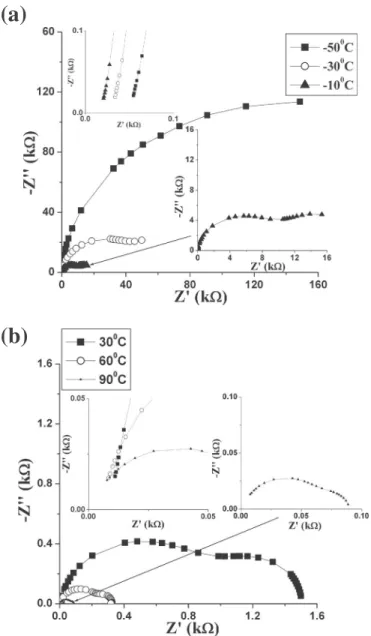
the angular frequency. Note that this model has assumed that the grains, domain boundaries, and grain boundaries are uni- formly distributed. Figure 4 shows the complex impedance 共Z*= Z⬘+ iZ⬙兲 plane plots of CaSiO3-doped CCTO at differ- ent measuring temperatures. Z⬘and Z⬙ for each RC element can be expressed as
Z⬘= R
1 +共RC兲2 共2兲
and
Z⬙= R冋1 +共RCRC兲2册. 共3兲
When the data of Z⬘ and Z⬙ are plotted by complex plane method and on a linear scale, they usually take the form of semicircles and spikes. It can be observed in Fig.4that there
are two distinguishable arcs, and they will be assumed to be perfect semicircles. In fact, there are supposed to be three semicircles present but the very high frequency one, belong- ing to grains, does not reveal. The value of R may be deter- mined from the intersections of the semicircles with Z⬘axes.
The R values of low- and high-frequency semicircles being able to be well defined at the measuring temperatures have been presented in Fig.5. It can be observed that these two R values decrease with increasing temperature, and the values of the low-frequency semicircle drop more quickly. The R values of the low- and high-frequency semicircles deter- mined at room temperature are 600 and 890⍀, respectively.
The effective resistance 共including the grain resistance, 10⍀兲 is 1500 ⍀, which is in agreement with the measured room-temperature bulk dc resistance 共1400 ⍀兲 of CaSiO3-doped CCTO. It, however, is much lower than the undoped CCTO共⬎105⍀兲.14,16In view of the occurrence of two semicircles, the presence of the domain boundaries in addition to the grain boundaries is assumed as suggested before.14–16 Nevertheless, it would be of importance to find out to which arc in the complex impedance plot the domain- boundary or grain-boundary response belongs. The activa- tion energy共E兲 of the temperature dependence of these two resistivity values is expected to be helpful in making a deci- sion. The Evalues have been evaluated from the Arrhenius plots共Fig.6兲 of ln共is the conductivity兲 versus 1/T 共T is the temperature兲. The obtained E values are 0.48 and 0.42 eV for the low- and high-frequency semicircles, respec- tively. The activation energy 共0.42 eV兲 for the high- frequency semicircle is comparable to 0.34 eV for undoped polycrystalline CCTO16 and is attributed to the domain- boundary response. For the low-frequency semicircle, though the E value 共0.48 eV兲 is lower than 0.63 eV of the undoped CCTO,14 it can be assigned to the grain-boundary response. The lower grain-boundary activation energy is re- lated to the change of the grain-boundary compositions and would be further evidenced by the following microstructure characterization.
(b)
FIG. 4. Complex impedance plane plots of CaSiO3-doped CCTO at different measuring temperatures共solid lines are drawn as a guide for the eyes兲.
-20 0 20 40 60 80 100 120
Res
10Temperature (
0C)
FIG. 5. Comparison of the temperature-dependent resistivity values of grain boundaries and domain boundaries.
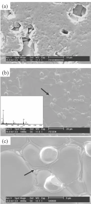
The comparison of microstructures of the undoped and CaSiO3-doped CCTO is shown in Fig.7. It can be observed that the microstructure of CaSiO3-doped CCTO contains a lot of second-phase particles in the grain edges or corners and a liquidlike second phase covering several grain bound- aries关Fig.7共b兲兴. The latter is magnified in Fig.7共c兲, and the thicknesses of the grain-boundary phases are in the range from 1 to 0.2m. The second-phase particles are rich in Cu, determined by the EDS spectrum关see the inset in Fig.7共b兲兴.
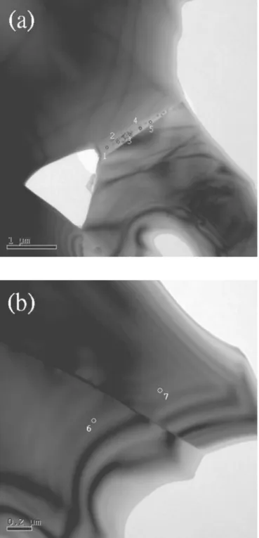
To prove that the Si ions segregate to the grain boundaries, the locations of the Si ions in CaSiO3-doped CCTO are fur- ther analyzed by HRAEM equipped with EDS. Several grains and grain boundaries were characterized and the typi- cal micrographs are illustrated in Fig. 8. 关The very wide grain boundary in Fig.8共a兲 essentially conforms to what is 共shown by an arrow兲 revealed in the SEM micrograph of Fig.
7共c兲.兴 It is observed that the grain-boundary phases contain a major second phase and a few nanosized particles. The former is further identified as an amorphous phase 共not shown兲, which possibly is a liquid phase, that forms at high temperatures and wets along the grain boundaries. It is fur- ther shown in Table I that the amorphous phase contains much higher concentration of the Si ions, indicating that the main phase is Si rich, whereas no Si ions can be detected in the grains. This proves that the Si ions indeed segregate to the grain boundaries. It also shows that though the nanosize particles are Cu rich, the average concentration of the Cu ions present in the grain boundaries is about 28 mol %, which is significantly lower than that of the undoped CCTO 共⬎70 mol%兲.26In light of the lower concentration of the Cu ions in the grain boundaries and the presence of the Cu-rich second-phase particles in the grain edges or corners, Si ions are suggested to inhibit the Cu ions to segregate to the grain boundaries. This suggestion is also supported by the fact that the amount of Cu-rich particles increases with the concentra- tion of the Si ions21 though the detailed mechanism is un- known. In the previous works,14,16,26 we have provided evi- dences that the excess Cu ions located at the grain boundaries are responsible for the enhancement of the grain-
boundary resistivity. Thus, the lowering of the grain- boundary resistivity in this investigation can be attributed to the much lower concentration of the excess Cu ions than undoped CCTO.26This not only indicates that the bulk resis- FIG. 6. Arrhenius plot of ln 共 is the conductivity兲 versus 1/T
共T is the temperature兲 for grain boundaries and domain boundaries.
FIG. 7. Comparison of the microstructures of共a兲 undoped and 共b兲 CaSiO3-doped CCTO, in which the second-phase particles, in- dicated by an arrow, are characterized by EDS共inset兲 and shown to be Cu rich. 共c兲 is the magnification of 共b兲 to manifest the grain- boundary phase, indicated by an arrow.
tivity of undoped CCTO is determined by the grain-boundary resistivity but also implies that the domain-boundary resis- tivity is not high. The latter is supported by the reported resistivity about 2.3⫻104⍀ cm at 289 K of the single- crystal CCTO,8which, however, is not in agreement with the suggestion of Shao et al.24who have proposed that domain- boundary resistivity should be higher than grain-boundary resistivity. Moreover, since the grain-boundary thickness 共though nonuniform兲 of CaSiO3-doped CCTO is much larger
than that of the undoped one 共1.7–2.9 nm兲,26 the lower grain-boundary resistance, obviously, should not be deter- mined by the grain-boundary thickness.
Regarding the main reason for the grain-boundary resis- tivity of CCTO, it has been considered to arise from the Schottky barriers,27like in the internal barrier capacitors and varistors, in which the grain-boundary defects are created by deliberately incorporated impurities. However, it is not so for CCTO since the only related main grain-boundary defect is the excess Cu ions.14,16 A space-charge defect model28 is suitable for this case. It is assumed that the excess Cu ions would develop positive grain-boundary surface charges and induce a space-charge layer. The induced space-charge layer is accompanied by a negative potential. In the negative space-charge potential, defects of negative effective charge such as acceptors and electrons are accumulated, and they may act as a barrier for the electrical conduction and deter- mine the grain-boundary resistivity. The much lower grain- boundary resistivity in CaSiO3-doped CCTO can be attrib- uted to the lower space-charge potential due to the significant reduction of the average concentration of the surface charges 共excess Cu ions兲 in the grain boundaries as compared to un- doped CCTO. Furthermore, if the electrons or holes are able to surmount this potential barrier, then the resistivity is ex- pected to decrease. Because of the nonuniform distribution of the surface charges共excess Cu ions兲 in the grain bound- aries, the charge carriers would surmount the barrier height wherever the space-charge potential lower than the thermal energy at high temperatures is. This provides the plausible reason for the declination of the dielectric constant in Fig.
3共a兲. On the other hand, it also causes the high conduction loss. The rapid increase of the dissipation factor shown in Fig.3共b兲supports this viewpoint. The ultrahigh static grain- boundary capacitance can also be rationalized by the space- charge model. According to the brick-layer model,29 the grain-boundary capacitance is usually considered to be in- versely proportional to its thickness. However, it apparently should depend on the space-charge-layer thickness instead of the grain-boundary thickness because the latter in CaSiO3-doped CCTO关referring to Figs.7and8共a兲兴 is much larger than that in undoped CCTO.26
FIG. 8. HRAEM micrographs of CaSiO3-doped CCTO. The circles in共a兲 for a grain boundary and in 共b兲 for the grains are the positions for the composition analyses characterized by EDS, and the results are summarized in TableI.
4 1.5 17.2 2.9 78.4
5 5.8 7.8 6.3 80.1
Average 2.5 28.3 3.4 65.9
6 14.1 34.7 51.2 0
7 13.0 34.8 52.2 0
There are two reasons for the higher-dielectric-constant relaxation with larger relaxation time not to be considered as electrode effect. First, this relaxation is material and tem- perature dependent and only observed for the CCTO sample with low resistivity 共⬍106⍀ cm, e.g., at high measuring temperatures for undoped CCTO24,25 and CaSiO3-doped CCTO in this investigation兲. Second, the electrode effect has been minimized by using the In-Ga electrode.27In addition, it has been reported30 that an extra low-frequency arc may stem from the very different grain-boundary conductivity when the conductivity ratio approaches zero. Though the grain-boundary composition in CaSiO3-doped CCTO is in- homogeneous, it is not expected that the difference of the resistivity between the grain boundaries would be in that extreme.
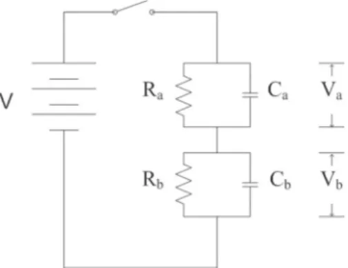
Actually, the lowering of the grain-boundary resistivity would provide not only a way for manifestation of the domain-boundary response but also an evidence for the pres- ence of domain boundaries in CCTO. If the grain boundaries would have much higher resistance like in undoped CCTO, the space-charge polarization of the domain boundaries would become negligible. This can be explained by less volt- age drop across the domain boundaries as follows. Under the condition of RgbⰇRdb⬎Rg, we neglect the element of the grains and consider only the elements of grain boundaries and domain boundaries. The equivalent circuit is illustrated in Fig.9, and the voltage drop across each element can be expressed as follows:23
Va= V Ra
Ra+ Rb
再
1 −冉1 −CbRb冊e−t/冎
共4兲and
Vb= V Rb
Ra+ Rb
再
1 −冉1 −CaRa冊e−t/冎
, 共5兲where V is the voltage, R is the resistance, C is the capaci- tance, t is the time, andis the relaxation time. When t = 0, Va/ Vb= Cb/ Ca, indicating that initially, the largest voltage drop would develop across smaller capacitance. On the other hand, when t =⬁, Va/ Vb= Ra/ Rb, which indicates that a big
voltage drop would occur across the large resistance at the final stage. Therefore, if the grain-boundary resistance is much larger than the domain-boundary one, the main voltage drop would be across the grain boundaries. When the resis- tance of grain boundaries approaches that of domain bound- aries共like in the CaSiO3-doped CCTO兲, the significant volt- age drop would develop across domain boundaries and manifest their dielectric responses.
IV. CONCLUSIONS
The frequency-dependent dielectric behavior of CaSiO3-doped polycrystalline CCTO reveals two Maxwell- Wagner-type relaxations including insulating layers of grain boundaries and domain boundaries and semiconducting grains. The temperature-dependent behavior of the dielectric constant, measured at 1 kHz, is essentially derived from the frequency dependence of the dielectric constant of two su- perposed dielectric relaxations at different temperatures共Fig.
1兲. The complex impedance plots exhibit two semicircles.
The high- and low-frequency semicircles have been deter- mined to be the domain boundaries and the grain boundaries, respectively. This further confirms that the domain bound- aries are indeed present in polycrystalline CCTO. The ca- pacitance and resistivity of the grain boundaries are evi- denced to be higher than those of the domain boundaries.
Whenever the grain-boundary resistivity approaches the do- main boundaries, the domain-boundary response would be- come manifested. The activation-energy values of 0.48 and 0.42 eV obtained from the temperature dependences of the conductivity of CaSiO3-doped CCTO are lower than those reported in the literature, and they are assigned to the re- sponses of grain boundaries and domain boundaries, respec- tively. The grain-boundary phases have been identified and consist of a main amorphous Si-rich phase and a small amount of nanosize CuO particles. Si ions are not found in the grains. The second-phase particles located at the grain edges and corners of CaSiO3-doped CCTO are Cu rich. This is attributed to the fact that the Si ions segregate and inhibit the excess Cu ions to the grain boundaries. The lowering of the grain-boundary resistivity is attributed to the reduction of the concentration of the excess Cu ions along the grain boundaries. This is also the reason for the rapid increase of the dissipation factors or dielectric losses. The excess Cu ions at the grain boundaries, acting as surface charges and inducing the space-charge layer, play a key role in determin- ing the grain-boundary resistivity and capacitance. The de- crease of the dielectric constant in region III of Fig.3共a兲is attributed to the nonuniform distribution of the surface charges 共excess Cu ions兲 at the grain boundaries due to the fact that the thermal energy overpowers the space-charge po- tential as the temperature increases.
ACKNOWLEDGMENT
The authors appreciate the financial support from the Na- tional Science Council of Taiwan under Contract No. NSC- 92-2216-E-006-010.
FIG. 9. Equivalent circuit of two RC elements in series, used to illustrate the voltage drop across the elements.
B 67, 012103共2003兲.
6N. Kolev, R. P. Bontchev, A. J. Jacobson, V. N. Popov, V. G.
Hadjiev, A. P. Litvinchuk, and M. N. Iliev, Phys. Rev. B 66, 132102共2002兲.
7C. C. Homes, T. Vogt, S. M. Shapiro, S. Wakimoto, M. A. Sub- ramanian, and A. P. Ramirez, Phys. Rev. B 67, 092106共2003兲.
8J. Li, A. W. Sleight, and M. A. Subramanian, Solid State Com- mun. 135, 260共2005兲.
9A. Tselev, C. M. Brooks, S. M. Anlage, H. Zheng, L. Salamanca- Riba, R. Ramesh, and M. A. Subramanian, Phys. Rev. B 70, 144101共2004兲.
10D. C. Sinclair, T. B. Adams, F. D. Morrison, and A. R. West, Appl. Phys. Lett. 80, 2153共2002兲.
11T. B. Adams, D. C. Sinclair, and A. R. West, Adv. Mater.共Wein- heim, Ger.兲 14, 1321 共2002兲.
12M. H. Cohen, J. B. Neaton, L. He, and D. Vanderbilt, J. Appl.
Phys. 94, 3299共2003兲.
13J. Li, M. A. Subramanian, H. D. Rosenfeld, C. Y. Jones, B. H.
共1982兲.
21C. Y. Lin, M.S. thesis, National Cheng Kung University, 2005.
22E. A. Patterson, S. Kwon, C. C. Huang, and D. P. Cann, Appl.
Phys. Lett. 87, 182911共2005兲.
23Arthur von Hippel, Dielectrics and Waves 共Wiley, New York, 1954兲, p. 229.
24S. F. Shao, J. L. Zhang, P. Zheng, W. L. Zhong, and C. L. Wang, J. Appl. Phys. 99, 084106共2006兲.
25S. Ke, H. Huang, and H. Fan, Appl. Phys. Lett. 89, 182904 共2006兲.
26T. T. Fang and L. T. Mei, J. Am. Ceram. Soc. 90, 638共2007兲.
27T. B. Adams, D. C. Sinclair, and A. R. West, Phys. Rev. B 73, 094124共2006兲.
28Y. M. Chiang, D. Birnie III, and W. D. Kingery, Physical Ceram- ics共Wiley, New York, 1997兲, p. 156.
29A. J. Moulson and J. M. Herbert, Electroceramics共Wiley, West Sussex, 2003兲, p. 328.
30J. Fleig and J. Maier, J. Eur. Ceram. Soc. 19, 693共1999兲.