White and Red Organic Light-Emitting Diodes Using a
Phosphorescent Iridium Complex as a Red Dopant
Po-Ching Kao,a Sheng-Yuan Chu,a,b,zChien-Hung Chen,bHsin-Hsuan Huang,a Cheng-Hsien Yang,c,dand I-Wen Sunc,d,
*
a
Department of Electrical Engineering,bInstitute of Micro-Electro-Mechanical-System Engineering,cDepartment of Chemistry, and dDepartment of Materials Science and Engineering, National Cheng-Kung University, Tainan 701-01, Taiwan
In this paper, we describe the phosphorescent characteristics of a red-emitting iridium complex, bis 共2-naphthalen-1-yl-5-trifluoromethyl-pyridine-N,C2兲iridium共III兲 acetylacetonate 关共5-fnapy兲
2Ir共acac兲兴, together with investigating the
electrolumines-cence共EL兲 mechanisms of organic light-emitting diodes 共OLEDs兲 by using this complex as a red dopant. A bright white and red light emission can be realized using the indium tin oxide/␣-naphthylphenylbiphenyl 共NPB兲/4,4⬘-N,N⬘-dicarbazole-biphenyl共CBP兲 共5-fnapy兲2Ir共acac兲/BAlq3/LiF/Al structure with different concentrations of共5-fnapy兲2Ir共acac兲 in CBP host. With the dopant
concentration above 9%, the red emission with Commission Internationale De L’Eclairage共CIE兲 coordinates x = 0.65, y = 0.34, maximum luminance of 7240 cd/m2and luminous efficiency of 7.1 cd/A was obtained in the device. The white-emitting device
with a maximum luminance of 3060 cd/m2 and maximum luminous efficiency of 4.0 cd/A was obtained via doping 1.5%共5
-fnapy兲2Ir共acac兲. The white-emission spectrum of this device is composed of a red band from 共5-fnapy兲2Ir共acac兲 and two blue emissions from NPB and BAlq3. The CIE coordinates were well within the white zone, which moves slightly from共0.33, 0.32兲 to
共0.36, 0.33兲 when applied voltage is varied from 9 to 18 V.
© 2006 The Electrochemical Society. 关DOI: 10.1149/1.2358930兴 All rights reserved.
Manuscript submitted April 24, 2006; revised manuscript received August 4, 2006. Available electronically October 16, 2006.
White organic light-emitting devices 共WOLEDs兲 have been drawing great interest because of their high luminance, low driving, and high efficiency, which can be used as backlights in flat-panel display and eventually as illumination light sources. Recently, highly efficient OLEDs and WOLEDs using phosphorescent mate-rials with incorporated heavy metal complexes have been reported.1-3Apart from fluorescent OLEDs which utilize only the singlet excitons, phosphorescent OLEDs have proven to be poten-tially more efficient because they can harvest both singlet and triplet excitons and have the potential of reaching a maximum internal efficiency of 100%.4-6In order to optimize device efficiency up to a theoretical limit, these heavy metal complex emitters have been doped into a layer of charge-transporting hosts such as 4,4
⬘
-N,N⬘
-dicarbazole-biphenyl 共CBP兲 or another host.7-9Because of an efficient transfer of both singlet and triplet excited states in the host to dopant, there is an increase of the internal efficiency.5 In addition, diluting the molecules into the host matrix also results in a decrease of triplet–triplet共T–T兲 annihilation.10,11Among all phosphorescent materials, iridium metal complexes containing the 2-phenylpyridyl共ppy兲 type of chelating ligands are the most famous materials due to the relatively short lifetime of their triplet state. In this article, we demonstrate and characterize white and red emission of OLEDs based on a red-emitting iridium complex, bis 共2-naphthalen-1-yl-5-trifluoromethyl-pyridine-N,C2兲iridium共III兲 acetylacetonate 关共5-fnapy兲2Ir共acac兲兴, with the
corresponding Commission Internationale De L’Eclairage共CIE兲 co-ordinates weakly dependent on the voltage. Compared with multilayers,12,13multidopants,14,15or other complicated structures,16 the WOLEDs prepared in our work have a simple three-layer struc-ture. The white emission can be achieved using the combination of several emission zones.3,17It is believed that simpler structure and voltage-independent WOLEDs are beneficial to the industrialization of WOLEDs displays.
Experimental
The indium tin oxide共ITO兲-coated glass substrates 共Merck Dis-play Technologies兲 used have a film thickness of 0.2 m and sheet resistance of approximately 15⍀/䊐. Molecular structures of the organic materials and the configuration of OLEDs used in this study are shown in Fig. 1. The共5-fnapy兲2Ir共acac兲 powders used in this
work are synthesized in the authors’ laboratory. All organic materi-als used were purified by a train sublimation. Prior to the organic films being deposited, the substrates were initially scrubbed in a detergent solution 共Merck Extran兲. They were then immersed se-quentially in a heated ultrasonic bath of deionized共DI兲 water, iso-propyl alcohol, and ethanol for 15 min each, followed by being rinsed in DI water. Finally, the substrates were blown dry with ni-trogen gas and then treated by UV ozone for 5 min prior to use. Electroluminescent devices have the following configurations: ITO/ ␣-naphthylphenylbiphenyl diamine 共NPB兲 共50 nm兲/CBP:共5-fnapy兲2Ir共acac兲 共50 nm兲/4-biphenyloxolato
aluminum共III兲bis共2-methyl-8-quinolinato兲4-phenylphenolate 共BAlq3兲 共50 nm兲/lithium
fluoride共LiF兲 共1 nm兲/Al 共150 nm兲. In the devices, NPB served as
*Electrochemical Society Active Member.
z
E-mail: [email protected]
Figure 1. Molecular structures of organic materials and the configuration of
OLEDs used in the experiment. Journal of The Electrochemical Society, 153共12兲 H228-H231 共2006兲
0013-4651/2006/153共12兲/H228/4/$20.00 © The Electrochemical Society
H228
the hole-transporting layer, BAlq3as the electron-transporting layer, and LiF/Al layers served as the composite cathode to enhance the electron injection efficiency. The concentrations of 共5-fnapy兲2Ir共acac兲 are changed from 1.5 to 10 wt % in different de-vices. All organic layers and the cathode were deposited by a resis-tive heating method. The deposition rate was controlled by a cali-brated quartz crystal oscillator and was maintained at 0.5 ± 0.2 Å/s for the organic materials, 0.1 Å/s for LiF, and 5 ± 2 Å/s for Al. The base pressure in the chamber was about 5⫻ 10−6Torr. A shadow
mask was used for the deposition of the cathode. The active area of the devices is 2⫻ 2 mm.
The highest occupied molecular orbital 共HOMO兲 and lowest unoccupied molecular orbital 共LUMO兲 energy levels of the 共5-fnapy兲2Ir共acac兲 were determined by using the photoelectron
spec-troscopy共Riken Keiki AC-2兲 and absorption spectroscopy 共Hitachi U-4100兲 measurements of the thin film. The photoluminescence 共PL兲 spectra were measured with a spectrometer 共Hitachi 850兲. The current-density-luminance-voltage characteristics of the devices were measured both with a source meter共Keithley-2400兲 and a lu-minance meter共Minolta LS-100兲. The EL spectra and CIE coordi-nates of the devices were measured by a spectrometer共PR650兲 and a source meter. All measurements were carried out at room tempera-ture and under ambient conditions without any protective coating.
Results and Discussion
Figure 2 shows the optical absorption and PL spectrum of 共5-fnapy兲2Ir共acac兲 in CH2Cl2solution 共1 ⫻ 10−3M兲 and in thin film
and the PL spectrum of CBP in thin film. The intense absorption peak bands in the UV region are assigned to the allowed singlet state -*transition of 2-共1-naphthalen兲 pyridine ligand. Weak
absorp-tion bands between 440 and 540 nm can be assigned to higher spin-allowed singlet metal-to-ligand charge transfer 共1MLCT兲 mixed with lower spin-forbidden triplet transitions3MLCT. A similar dis-cussion has been previously used for the analogous cyclometalated iridium complexes in the literature.18,19 Compared to the corre-sponding absorption spectrum of Ir共ppy兲3, the peak of-*
transi-tion from共5-fnapy兲2Ir共acac兲 has a red-shifted peak at approximately 25 nm.18Upon photoexcitation, the neat共5-fnapy兲2Ir共acac兲 thin film
emitted a red light peaked at 616 nm with a shoulder at 660 nm. The emission spectrum for a neat thin film of 共5-fnapy兲2Ir共acac兲 is broader than that for a solution of共5-fnapy兲2Ir共acac兲. The
broaden-ing in neat of共5-fnapy兲2Ir共acac兲 is presumably due to solid-state
solvation effects共SSSE兲 in the amorphous thin film.20In addition, from the PL spectrum of the host CBP and the absorption spectrum of the guest共5-fnapy兲2Ir共acac兲, a large spectral overlap for the
ef-ficient Förster energy transfer between the guest and hosts is shown.
Förster transfer is a resonant dipole coupling process that transfers energy between singlet states. The probability of Förster energy transfer was predicted by the calculation of Förster transfer radius from absorption spectrum of a guest and emission spectrum of a host.21There is no emission of the host CBP in the EL spectrum 共Fig. 3兲, also indicating the Förster transfer is an efficient mecha-nism here.
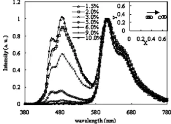
Figure 3 shows the normalized EL spectrum of OLEDs based on 共5-fnapy兲2Ir共acac兲 with different concentrations in CBP. As can be
seen, red emission at around 612 nm with a shoulder at about 660 nm is attributed to the phosphorescence of共5-fnapy兲2Ir共acac兲, which coincides with the PL spectrum as shown in Fig. 2. It is noted that the replacement of phenylpyridine ligand in Ir共ppy兲2共acac兲22 by naphthylpyridine in 共5-fnapy兲2Ir共acac兲 leads to significant red
shift of the maximum emission wavelength from 525 nm for Ir共ppy兲2共acac兲-doped CBP devices to 612 nm for 共5-fnapy兲2Ir共acac兲-doped ones. This indicates that the variation of
- conjugate of cyclometalated ligand in orthometalated complex and the introduction of trifluoromethyl group could influence the emission properties of the corresponding iridium complex.23 The substituent of the trifluoromethyl group on the cyclometalated Ir共III兲 complexes has been shown to have a stronger influence on lowering the LUMO levels.24There exist blue emissions centering at around 448 and 484 nm with a shoulder at about 512 nm when the doping concentration is low. The former peak comes from the emission of NPB25and the latter peak with a shoulder comes from BAlq3.26The CIE coordinates of these devices共inset of Fig. 3兲 show that along with the increasing of the共5-fnapy兲2Ir共acac兲 doping concentration,
the CIE coordinates of the devices move towards the red region. Figure 4 shows the proposed energy level diagram of the device studied, with the relative alignment of the HOMO and LUMO levels of each layer. According to the energy level diagram, the red emis-sion has two possible excitation ways: not due to the energy transfer from CBP, but from the direct recombination of injected carriers at the red dopant sites. As the concentration of共5-fnapy兲2Ir共acac兲 is
low, the number of carriers trapping on 共5-fnapy兲2Ir共acac兲 mol-ecules is less. Thus, more excitons may form at NPB/CBP and CBP/BAlq3interfaces and recombine in the NPB and BAlq3layers, resulting in an increased emission from NPB and BAlq3. When
increasing the concentration of the共5-fnapy兲2Ir共acac兲 the intensity
of the red emission increases relative to the blue emission. This is attributed to more trapped carriers on共5-fnapy兲2Ir共acac兲 molecules or the increased energy transfer from CBP to 共5-fnapy兲2Ir共acac兲. The CIE coordinates of the devices with 1.5 and 9% 共5 -fnapy兲2Ir共acac兲 are 共0.33,0.32兲 and 共0.65, 0.34兲, respectively. The
Figure 2. Optical absorption and PL spectra of共5-fnapy兲2Ir共acac兲 in CH2Cl2 solution and in thin film, and PL spectra of CBP in thin film. The 325 nm
line from a mercury lamp is used as the excitation source. Figure 3. Normalized EL spectrum of the devices with various 共5-fnapy兲2Ir共acac兲 doping concentrations in the 50 nm thick CBP and their CIE
coordinates共inset of Fig. 3兲.
H229
Journal of The Electrochemical Society, 153共12兲 H228-H231 共2006兲 H229
former is fairly close to the white-light equienergy point共0.33, 0.33兲 and the latter near the National Television System Committee 共NTSC兲 standard red point 共0.66, 0.33兲.
Figure 5a and b shows the normalized EL spectrum of the device at different applied voltages for the white-emission and red-emission devices with 1.5 and 9%共5-fnapy兲2Ir共acac兲 in CBP and their CIE coordinates. It is found that the white device shows a decrease in the relative intensity of blue-to-red emission with the increase of the driving voltage. As the driving voltage increases, more carriers can
overcome the injection barriers and recombine in the doped CBP layer. Thus, it leads to the increase of the共5-fnapy兲2Ir共acac兲
emis-sion relative to the blue emisemis-sion. However, it is obvious that the emission spectra is changed a little at different driving voltages and the CIE coordinates are well within the white region, which the CIE coordinates change slightly from共0.33, 0.32兲 at 9 V to 共0.36, 0.33兲 at 18 V. Figure 4b shows no change in the EL spectra for the red-emission device with the increase of the driving voltage.
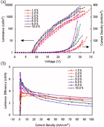
Figure 6 shows the current-density-luminance–voltage共Fig. 6a兲 and luminous-efficiency–current density共Fig. 6b兲 characteristics for CBP:共5-fnapy兲2Ir共acac兲 devices with different doping concentra-tions of共5-fnapy兲2Ir共acac兲. As in the case of other phosphorescent
OLEDs and PLEDs, the device performance shows a strong depen-dence on the doping concentration. When the doping concentration is higher than 5%, the current density increases apparently at the same voltage. The change in the current density may be explained as follows. At low共5-fnapy兲2Ir共acac兲 concentration, carrier transport is
controlled by the slow release of carriers from共5-fnapy兲2Ir共acac兲 molecules acting as traps. It then leads to lower current density. However, two effects may arise at higher共5-fnapy兲2Ir共acac兲 con-centration. One possible effect is that the increase in dopant concen-tration induces the band bending due to the traps and favors charge injection into the CBP layer.27The other possible effect is that both materials共dopant and host兲 rather than only the host material par-ticipate in transport because the distance between the 共5-fnapy兲2Ir共acac兲 molecules becomes shorter.28They then both lead to
higher current density. Because the change in current density is cor-related with the concentration of dopant, the doped 共5-fnapy兲2Ir共acac兲 could be regarded as an efficient trap for the injected carriers and the charge trapping mechanism should be considered.25,29-31 The HOMO and LUMO energy levels of 共5-fnapy兲2Ir共acac兲 were determined to be −5.6 and −3.5 eV, which were within the levels of CBP, suggesting this mechanism was
Figure 4. Schematic of energy level diagram of the 共5-fnapy兲2Ir共acac兲-doped OLEDs.
Figure 5. Normalized EL spectrum of the device at different applied
volt-ages for共a兲 white emission and 共b兲 red emission devices and their CIE coordinates共inset of Fig. 5兲.
Figure 6. 共a兲 共Color online兲 Current-density-luminance–voltage and
共b兲 luminous-efficiency–current-density characteristics of the 共5-fnapy兲2Ir共acac兲-doped OLEDs with different concentration of
共5-fnapy兲2Ir共acac兲 ranging from 1.5 to 10%.
H230 Journal of The Electrochemical Society, 153共12兲 H228-H231 共2006兲
H230
reasonable. Due to the existence of barriers at NPB/CBP and CBP/BAlq3 interfaces, it would cause higher turn-on voltages
共⬃8 V兲 in the devices. The device which has a 共5-fnapy兲2Ir共acac兲-doped CBP with 9% doping concentration achieved the best performance with the maximum luminance of 7240 cd/m2 and the maximum luminous efficiency of 7.1 cd/A. With the in-crease of current density to 100 mA/cm2, however, a significant
decrease of the luminous efficiency to 3.1 cd/A is observed and can be explained by T–T annihilation.6The white-emitting device with 1.5% doping concentration has the maximum luminance of 3060 cd/m2and luminous efficiency of 4.0 cd/A, respectively.
Conclusions
In conclusion, we have investigated phosphorescent characteris-tics of a new red-emitting iridium complex,共5-fnapy兲2Ir共acac兲, and
fabricated the white- and red-emission OLEDs with promising de-vice characteristics by using this complex as a dopant. The use of CBP:共5-fnapy兲2Ir共acac兲 layer inserted between the NPB and BAlq3 layers was demonstrated to produce pure white emission via doping 1.5% 共5-fnapy兲2Ir共acac兲 and deep red emission when the doped concentration is above 9%. The effective energy transfer from CBP host to 共5-fnapy兲2Ir共acac兲 guest and the direct recombination of
electron-hole pairs on dopants were confirmed and a maximum lu-minance efficiency of 7.1 cd/A was achieved in these electrophos-phorescent OLEDs. The devices used in this work have a simple structure and their CIE coordinates are changed slightly by the driv-ing voltages. Further optimization of device efficiencies by utilizdriv-ing other host layers is in progress.
Acknowledgments
We acknowledge the financial support provided by the National Science Council under grant no. NSC-94-2215-E-006-008. We also thank the Center for Micro-Nano-Technology, National Cheng-Kung University, for providing the Single-Side Mask Aligner共OAI, J500兲.
National Cheng Kung University assisted in meeting the publication costs of this article.
References
1. M. A. Baldo, D. F. O’Brien, Y. You, A. Shoustikov, S. Sibley, M. E. Thompson, and S. R. Forrest, Nature (London), 395, 151共1998兲.
2. G. Cheng, F. Li, Y. Duan, J. Feng, S. Liu, S. Qiu, D. Lin, Y. Ma, and S. T. Lee,
Appl. Phys. Lett., 82, 4224共2003兲.
3. F. Li, G. Cheng, Y. Zhao, J. Feng, S. Liu, M. Zhang, Y. Ma, and J. Shen, Appl.
Phys. Lett., 83, 4716共2003兲.
4. T. Tsuzuki, N. Shirasawa, T. Suzuki, and S. Tokito, Adv. Mater. (Weinheim, Ger.),
15, 1455共2003兲.
5. M. A. Baldo, S. Lamansky, P. E. Burrows, M. E. Thompson, and S. R. Forrest,
Appl. Phys. Lett., 75, 4共1999兲.
6. C. Adachi, M. A. Baldo, S. R. Forrest, S. Lamansky, M. E. Thompson, and R. C. Kwong, Appl. Phys. Lett., 78, 1622共2001兲.
7. C. Adachi, R. Kwong, and S. R. Forrest, Org. Electron., 2, 37共2001兲. 8. S. Lamansky, P. I. Djurovich, F. Abdel-Razzaq, S. Garon, D. L. Murphy, and M. E.
Thompson, J. Appl. Phys., 92, 1570共2002兲.
9. S. Tokito, T. Iijima, Y. Suzuri, H. Kita, T. Tsuzuki, and F. Sato, Appl. Phys. Lett.,
83, 569共2003兲.
10. J. P. Duan, P. P. Sun, and C. H. Cheng, Adv. Mater. (Weinheim, Ger.), 15, 224 共2003兲.
11. C. H. Yang, K. H. Fang, W. L. Su, S. P. Wang, S. K. Su, and I. W. Sun, J.
Organomet. Chem., 691, 2767共2006兲.
12. C. H. Kim and J. Shinar, Appl. Phys. Lett., 80, 2201共2002兲.
13. B. W. D’Andrade, M. E. Thompson, and S. T. Forrest, Adv. Mater. (Weinheim,
Ger.), 14, 147共2002兲.
14. J. Kido, H. Shionoya, and K. Nagai, Appl. Phys. Lett., 67, 2281共1995兲. 15. Y. Kawamura, S. Yanagida, and S. R. Forrest, J. Appl. Phys., 92, 87共2002兲. 16. A. Dodabalapur, L. J. Rothberg, and T. M. Miller, Appl. Phys. Lett., 65, 2308
共1994兲.
17. D. Qin and Y. Tao, Appl. Phys. Lett., 86, 113507共2005兲.
18. K. A. King, P. J. Spellane, and R. J. Wattes, J. Am. Chem. Soc., 107, 1431共1985兲. 19. M. G. Colombo, T. C. Brunold, T. Riedener, H. U. Gudel, M. Fortsch, and H.-B.
Burgi, Inorg. Chem., 33, 545共1994兲.
20. V. Bulovic, R. Deshpande, M. E. Thompson, and S. R. Forrest, Chem. Phys. Lett.,
308, 317共1999兲.
21. T. Förster, Discuss. Faraday Soc., 27, 7共1959兲.
22. S. Lamansky, P. Djurovich, D. Murphy, F. Adbel-Razzaq, H.-E. Lee, C. Adachi, P. E. Burrows, S. R. Forrest, and M. E. Thompson, J. Am. Chem. Soc., 123, 4304 共2001兲.
23. A. Tsuboyama, H. Iwawaki, M. Furugori, T. Mukaide, J. Kamatani, S. Igawa, T. Moriyama, S. Miura, T. Takiguchi, S. Okada, M. Hoshino, and K. Ueno, J. Am.
Chem. Soc., 125, 12971共2003兲.
24. F. M. Hwang, H. Y. Chen, P. S. Chen, C. S. Liu, Y. Chi, C. F. Shu, F. I. Wu, P. T. Chou, S. M. Peng, and G. H. Lee, Inorg. Chem., 44, 1344共2005兲.
25. J. T. Lim, C. H. Jeong, J. H. Lee, J. H. Lim, and G. Y. Yeom, Jpn. J. Appl. Phys.,
Part 1, 45, 1826共2006兲.
26. J. H. Niu, W. L. Li, H. Z. Wei, M. T. Li, W. M. Su, Q. Xin, Z. Q. Zhang, and Z. Z. Hu, J. Phys. D, 38, 1136共2005兲.
27. E. G. Thianche, C. Sentein, A. Lorin, C. Denis, P. Raimond, and J. M. Nunzi, J.
Appl. Phys., 83, 4236共1998兲.
28. H. Murata, C. D. Merritt, and Z. H. Kafafi, IEEE J. Sel. Top. Quantum Electron., 4, 119共1998兲.
29. N. Matsusue, S. lkame, Y. Suzuki, and H. Naito, J. Appl. Phys., 97, 123512共2005兲. 30. C. Qiu, Z. Xie, H. Chen, B. Z. Tang, M. Wong, and H. S. Kwok, IEEE J. Sel. Top.
Quantum Electron., 10, 101共2004兲.
31. F. Nuesch, D. Berner, E. Tutis, M. Schaer, C. Ma, X. Wang, B. Zhang, and L. Zuppiroli, Adv. Funct. Mater., 15, 323共2005兲.
H231
Journal of The Electrochemical Society, 153共12兲 H228-H231 共2006兲 H231