Effect of GaN cap layer grown at a low temperature on electrical
characteristics of Al
0.25Ga
0.75N / GaN heterojunction field-effect transistors
C. J. KaoDepartment of Physics, National Central University, Chung-Li 32054, Taiwan
J. K. Sheua)
Institute of Electro-optical Science and Engineering, National Cheng Kung University, Tainan 70101, Taiwan
W. C. Lai and M. L. Lee
Institute of Microelectronics, Department of Electrical Engineering, National Cheng Kung University, Tainan 70101, Taiwan
M. C. Chen and G. C. Chi
Department of Physics and Institute of Optical Science, National Central University, Chung-Li 32054, Taiwan
(Received 20 January 2004; accepted 16 June 2004)
This study examined the effect of GaN grown by metalorganic vapor phase epitaxy at low temperature 共LT-GaN兲 on the surface of Al0.25Ga0.75N / GaN heterostructures. Depositing a
high-resistivity LT-GaN surface layer on the Al0.25Ga0.75N / GaN heterostructures increased both the
sheet carrier concentrations and the electron mobility. This enhancement changed when the LT -GaN high-resistivity layer was removed by high-density-plasma etching. These observations are attributable to the passivation effect, implying that the LT-GaN behaves like a dielectric film, such as silicon dioxide, to passivate the surface states, yielding a different, maybe lower, electronic density of states than that of the Al0.25Ga0.75N free surface. Hall-effect measurement and gate lag
measurement were performed on the field-effect transistor devices to clarify the effect of LT -GaN cap layer on Al0.25Ga0.75N / GaN heterostructures. © 2004 American Institute of Physics.
[DOI: 10.1063/1.1784038]
The outstanding performance of AIGaN/ GaN hetero-structure field-effect transistors (HFETs) operated at high power and high temperature is widely recognized.1 Perfor-mance at high-power and high temperatures can be improved by reducing gate leakage current, specifically at high volt-ages and elevated temperatures. An insulating gate layer can be used to achieve these results. To our knowledge, Si3N4, Ga2O3, Gd2O3, SiO2, Ta2O3, and polymer poly(PBT)
can all be used as the insulating material of nitride-based HFETs, but none of these insulating materials can be pre-pared by in situ process2–5 GaN grown at low temperature 共LT-GaN兲, which is commonly used as a nucleation layer on sapphire, has been shown to have poor crystalline quality.6It behaves quite differently from a typical high-temperature-grown GaN layer, so LT-GaN should be useable as a stable insulating gate layer for nitride-based HFETs. III-nitride-based HFETs with a high-resistivity LT-GaN cap layer have at least the advantage of a structure that does not require extra growth. steps to prepare dielectric films, so surface contamination can be prevented. Additionally, the electronic density of state in the AlGaN/ LT-GaN interface of the nitride-based HFETs with LT-GaN cap layer is lower than that of HFETs with an AlGaN free surface. Several groups have obtained similar results for the passivation effect of dielectric films on FETs.7,8 In this study, both the sheet carrier concentration and the electron mobility in the LT-GaN/ Al0.25Ga0.75N / GaN heterostructure are
substan-tially higher than that of the Al0.25Ga0.75N / GaN
heterostruc-ture, as will be discussed in detail.
All of the samples used in this study were grown on c-face (0001) sapphire substrates by metalorganic vapor phase epitaxy(MOVPE) reactor.9A 30-nm-thick GaN nucle-ation layer was first grown on the sapphire substrate at 560 ° C. The temperature was then raised to 1060 ° C to grow a 2-m-thick undoped GaN共n⬃3⫻1016cm−3兲 buffer layer.
A 50-nm-thick highly resistive Mg-doped GaN layer was subsequently grown on top of the buffer layer to eliminate the side gating effect and the substrate leakage current.10A 0.3-m-thick undoped GaN was then grown at 1060 ° C as a channel layer, followed by a 5-nm-thick undoped Al0.25Ga0.75N spacer and a 30-nm-thick Si doped
Al0.25Ga0.75N barrier layer 共n⬃1⫻1018cm−3兲. Finally, a
20-nm-thick LT-GaN high-resistivity cap layer was grown on top of the barrier layer at 560 ° C. The samples with this structure were called sample A. Samples without the LT -GaN cap layer were also prepared for comparison and called sample B. The Hall effect was measured by forming Van der Pauw patterns on these samples with dimensions of 5 mm ⫻5 mm. The area of the contacts on the samples was defined by lithography. The high-resistivity LT-GaN layer of each sample A was etched away using a Cl2-based
inductively-coupled-plasma etcher, and then depositing
Ti/ Al/ Ti/ Au共50/100/50/200 nm兲 metal contacts on the ex-posed Si-doped Al0.25Ga0.75N barrier layer.
Table I indicates that the sheet carrier concentrations共ns兲
and mobilities in samples A and B depend on temperature. According to previous reports,11–13the sheet charge density
a)Electronic mail: [email protected]
APPLIED PHYSICS LETTERS VOLUME 85, NUMBER 8 23 AUGUST 2004
0003-6951/2004/85(8)/1430/3/$20.00 1430 © 2004 American Institute of Physics
of 2DEG(two-dimension electron gas), ns,2DEGcan be tenta-tively described by ns,2DEG=pol e + AlGaN ed
冉
⌬Ec− Ef e −b冊
+ d 2Nd, 共1兲where e is the electronic charge andpolis the
polarization-induced sheet charges at the AlxGa1−xN / GaN heterointer-face. Nd, d, and AlGaN are the dopant concentration,
thick-ness, and dielectric constant of the AlxGa1−xN barrier layer,
respectively. ⌬Ec is the AlxGa1−xN / GaN conduction-band
offset; Ef is the Fermi energy at AlxGa1−xN / GaN interface,
and b is the potential difference between the Fermi level and the edge of the AlxGa1−xN / GaN conduction band at the
AlxGa1−xN / LT-GaN interface (sample A) or the AlxGa1−xN
free surface(sample B). Table I and Eq. (1) indicate that the LT-GaN cap layer increases the sheet carrier concentration by reducingb in the AlxGa1−xN / GaN heterostructure. This phenomenon was observed to be just like the SiNx or SiO2
insulating layer’s passivation of surface states at the AlxGa1−xN surface.
7
The Hall-effect measurements reveal that the LT-GaN cap layer of sample A has a resistivity that greatly exceeds 1011⍀/䊐. The LT-GaN is suggested to be a highly compensated material because deep acceptor states originate from the high density of defects in the structure. Further investigations are under way to confirm this claim. Therefore, this finding differs from that for the conventional GaN/ AlxGa1−xN / GaN heterostructure, for which the
high-temperature growth共⬃1100 °C兲 of a GaN cap layer reduces the 2DEG density.14
Table I indicates that LT-GaN cap layer can result in an increase of charge density at the Al0.25Ga0.75N / GaN
hetero-interface above that of the free surface structure of sample B. This result can be explained by the fact that the LT-GaN cap layer should be able to alter and/or reduce the electronic density of states at the Al0.25Ga0.75N surface.
7,8
The changes in carrier concentration and transport properties of sample A upon the removal of the LT-GaN cap layer is studied to clarify further the effect of the layer on the electrical charac-teristics of Al0.25Ga0.75N / GaN heterostructures. After the
samples were measured, the contact areas were masked off and then the LT-GaN cap layer etched away using Cl2-based plasma to eliminate sample-to-sample variation. When the LT-GaN cap layer was removed, yielding sample C, the Hall-effect measurement was repeated. The room-temperature sheet carrier concentrations of samples A and C are 1⫻10−13and 7.5⫻1012/ cm2, respectively. The value for
sample C slightly exceeds that for, sample B with the free Al0.25Ga0.75N surface. Based on the earlier assertion that the
electrical properties of AlGaN/ GaN heterostructure relate to surface state, this difference between these two samples (samples B and C) can be attributed to the difference be-tween surface states even if all samples have a free surface. Restated, the plasma etching process alters the surface state,
making it different from that of the as-grown surface of for example sample B. Therefore, samples A and C are com-pared to elucidate the passivation effect of LT-GaN on Al0.25Ga0.75N / GaN heterostructure. The enhancement of the
sheet carrier concentration should be reversible, so removing the LT-GaN cap layer eliminates the enhancement.
For FET processing, ion implantation of Mg ions into the samples for electrical isolation was first performed to define the active region of Al0.25Ga0.75N / GaN HFETs.
Plasma etching was performed on sample A to etch away the LT-GaN layer in the source/drain areas and then the Ti/ Al/ Ti/ Au共50/100/50/200 nm兲 multilayer metals were deposited onto the exposed Al0.25Ga0.75N layer to serve as
source/drain electrodes. Ni/ Au共100/100 nm兲 Schottky con-tacts were then deposited on the LT-GaN layer of the gate areas to serve as the gate electrodes. The length and the width of the gate of fabricated devices were 0.5 and 100m respectively. The processing of sample B was similar to that of sample A, but without the added dry etching process. In other words, the only difference was that the Schottky gate metal was deposited on top of the Al0.25Ga0.75N barrier layer
for sample B.
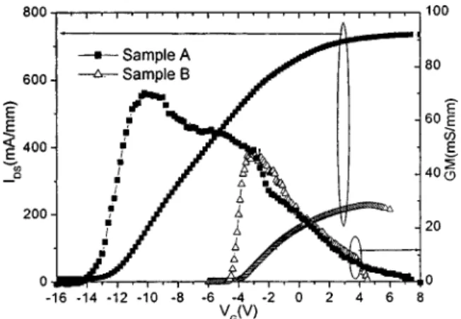
Samples A have a saturation drain current 共IDS兲 of
around 680 mA/ mm when VGS is 0 V, which greatly
ex-ceeds that of sample B, which have a saturation drain current 共IDS兲 of around 186 mA/mm when VGSis 0 V. This result is
attributable to the increase in both the carrier concentration and the mobility associated with the LT-GaN surface passi-vation layer, and is consistent with the Hall measurements; listed in Table I. The typical threshold voltages were around −14 and −5 V for samples A and B, respectively. The larger threshold voltage of sample A was attributable to the larger distance between the Schottky gate metal and the 2DEG channel layer, due to the insertion of the LT-GaN layer. Fig-ure 1 indicates that the maximum values of Idsswere 735 and
236 mA/ mm for samples A and B, respectively. The maxi-TABLE I. Electron mobility共兲 relative to sheet carrier concentration 共ns兲 were measured at different temperatures for samples A, B, and C.
Temperature(K) 95 205 295
Items ns共⫻1012cm−2兲 共 cm−2/ V s兲 ns共⫻1012cm−2兲 共cm−2/ V s兲 ns共⫻1012cm−2兲 共 cm−2/ V s兲
Sample A 9.4 2460 9.77 1770 10.3 1090
Sample B 5.7 1300 5.6 1110 5.4 829
Sample C 7.4 1230 7.4 1070 7.5 781
FIG. 1. Typical saturation current共Idss兲 and transconductance 共Gm兲 as a function of gate-source voltage for sample A and B, respectively.
Appl. Phys. Lett., Vol. 85, No. 8, 23 August 2004 Kaoet al. 1431
mum values of Gm were 70 and 48 mS/ mm for samples A and B, respectively. These figures clearly demonstrate that the dc performance of sample A is much better than those of sample B. In other words, the current driving ability sample A greatly exceeded that of sample B, because the former had a higher carrier concentration and higher carrier mobility. Additionally, the Gmprofile of sample A was much broader
than those of sample B, which is consistent with the fact that the Schottky gate metal in samples A was farther away from the 2DEG layer. The broad Gmprofile could in turn result in a larger gate voltage swing, improving the linearity and the dynamic range of power. Furthermore, gate lag measure-ments were made to clarify further the effect of LT-GaN cap layer on the Al0.25Ga0.75N / GaN HFETs. Gate lag is generally caused by surface states that act as electron traps in the ac-cess regions between the metal contacts, reducing the drain current. The trapped electrons deplete the 2DEG in the ac-cess regions of the device, limiting the drain current.15–17In the following measurements of gate lag, VGS was pulsed
from the threshold voltage, Vt, to 0 V, while VDSwas swept from 0 to 15 V. The period of pulsation was 50 ms, and the width of the pulse was 0.5 ms. Figures 2(a) and 2(b) present the measured gate lags for samples A and B, respectively. The drain current of samples A declined by 5% or less while sample B declined by around 30%. Theses results are con-sistent with the assumption that the LT-GaN cap layer can at last partially passivate surface states. This result is similar to
that obtained for AlGaN/ GaN HFETs with MgO and Sc2O3
passivation.8
In sum, the extent to which high-resistivity GaN grown by MOVPE at a low temperature affects Al0.25Ga0.75N / GaN heterostructures was studied. The LT-GaN cap layer in-creased both the sheet carrier concentrations and the electron mobility in the Al0.25Ga0.75N / GaN heterostructure, perhaps
by reducingbat the AlxGa1−xN / LT-GaN interface since the LT-GaN cap layer can alter and/or reduce the electronic den-sity of states at the Al0.25Ga0.75N surface. These results dif-fered from those of the GaN/ AlxGa1−xN / GaN
heterostruc-ture and are very similar to those devices with surface passivation by dielectric films. Furthermore, the findings in-dicate that the enhancement in the sheet carrier concentration is reversible, meaning that removing the LT-GaN cap layer eliminates it, implying that the Al0.25Ga0.75N / GaN interface
has a different, perhaps lower, electronic density of states than the Al0.25Ga0.75N free surface(sample B). However, the
Al0.25Ga0.75N / GaN HFETs with LT-GaN cap layer also
ex-hibited a better dc performance than the samples without LT-GaN cap layer.
The authors would like to thank the National Science Council of the Republic of China for financially supporting this research under Contract Nos. NSC 92-2218-E-008-012 and NSC 92-2215-E-008-018.
1
S. J. Pearton, J. C. Zolper, R. J. Shul, and F. Ren, J. Appl. Phys. 86, 1 (1999), and references therein.
2
F. Ren, M. Hong, S. N. G. Chu, M. A. Marcus, M. J. Schurman, A. Baca, S. J. Pearton, and C. R. Abernathy, Appl. Phys. Lett. 73, 3893(1998), and references therein.
3
M. A. Khan, X. Hu, A. Tarakji, G. Simin, J. Yang, R. Gaska, and M. S. Shur, Appl. Phys. Lett. 77, 1339(2000), and references therein. 4
L. W. Tu, P. H. Tsao, K. H. Lee, Ikai Lo, S. J. Bai, C. C. Wu, K. Y. Hsieh, and J. K. Sheu, Appl. Phys. Lett. 79, 4589(2001), and references therein. 5
T. R. Prunty, J. A. Smart, E. M. Chumbes, B. K. Ridley, L. F. Eastman, and J. R. Shealy, 2000 IEEE/Cornell Conference, p. 208, and references therein.
6
S. Nakamura, Jpn. J. Appl. Phys., Part 2 30, L1705(1991), and references therein.
7
X. Z. Dang, B. T. Yu, E. J. Piner, and B. T. McDermott, J. Appl. Phys. 90, 1357(2001).
8
B. Luo, J. W. Johnson, J. Kim, R. M. Mehandru, F. Ren, B. P. Gila, A. H. Onstine, C. R. Abernathy, and S. J. Pearton, A. G. Baca, R. D. Briggs, R. J. Shul, C. Monier, and J. Han, Appl. Phys. Lett. 80, 1661(2002). 9
J. K. Sheu, Y. K. Su, G. C. Chi, M. J. Jou, C. C. Liu, C. M. Chang, W. C. Hung, J. S. Bow, and Y. C. Yu, J. Vac. Sci. Technol. B 18, 729(2000). 10
F. W. Smith, A. R. Calawa, C. L. Chen, M. J. Manfra, and L. J. Mahoney, IEEE Electron Device Lett. 9, 77(1988).
11
E. T. Yu, X. Z. Dang, L. S. Yu, D. Qiao, P. M. Asbeck, S. S. Lau, G. J. Sullivan, K. S. Boutros, and J. M. Redwing, Appl. Phys. Lett. 73, 1880 (1998).
12
O. Ambacher, B. Foutz, J. Smart, J. R. Shealy, N. G. Weimann, K. Chu, M. Murphy, A. J. Sierakowski, W. J. Schaff, L. F. Eastman, R. Dimitrov, A. Mitchell, and M. Stutzmann, J. Appl. Phys. 87, 334(2000), and refer-ences therein.
13
B. Jogai, J. Appl. Phys. 91, 3721(2002). 14
B. Jogai, J. Appl. Phys. 93, 1631(2003). 15
H. Kim, R. M. Thompson, V. Tilak, T. R. Prunty, J. R. Shealy, and L. F. Eastman, IEEE Electron Device Lett. 24, 421(2003).
16
S. C. Binari, K. Ikossi, J. A. Roussos, W. Kruppa, D. Park, H. B. Dietrich, D. D. Koleske, A. E. Wickenden, and R. L. Henry, IEEE Electron Device Lett. 48, 465(2001).
17
B. Luo, J. Kim, F. Ren, J. K. Gillespie, R. C. Fitch, J. Sewell, R. Dettmer, G. D. Via, A. Crespo, T. J. Jenkins, B. P. Gila, A. H. Onstine, K. K. Allums, C. R. Abernathy, S. J. Pearton, R. Dwivedi, T. N. Fogarty, and R. Wilkins, Appl. Phys. Lett. 82, 1428(2003).
FIG. 2. Gate lag measurements were performed on(a) sample A and (b) sample B. The pulsed VGSwere varied from the threshold voltage, Vt, to 0 V while VDSwas sweeping from 0 to 15 V.
1432 Appl. Phys. Lett., Vol. 85, No. 8, 23 August 2004 Kaoet al.