Design and Implementation of a Retrofit LED
Lamp for AC Mains and Ballasts
Huan-Hao Chang, Tsorng-Juu Liang, Fellow, IEEE, Wei-Jing Tseng, and Li-An Hsu Department of Electrical Engineering/Advanced Optoelectronic Technology Center (AOTC)
/Green Energy Electronics Research Center (GREERC) National Cheng Kung University, Tainan, Taiwan
Email: [email protected]
Abstract—In this paper, the design and implementation of a
retrofit LED lamp for AC mains and ballasts is proposed. The proposed driver contains a simple technique to deal with the different kinds of sources between high frequency power from electronic ballasts and low frequency power from AC grid and electromagnetic ballasts. With this technology, the fluorescent lamp can be replaced with the proposed LED lamp without exchanging the existed lighting fixtures and the circuitry doesn’t need to be rewired, which will decrease the cost of change the entire system. The operating principles of the proposed LED lamp, the design consideration, and the key parameters will be discussed. Finally, a hardware prototype of a 22W retrofit LED lamp is built to verify the feasibility of the proposed method.
Index Terms---Retrofit, LED driver, Ballast. I. INTRODUCTION
Because of the rapid revolution in lighting-emitter-diode (LED) and white power LED technique, the demand of LED lighting source has become much more popular in the recent years [1]. A new evolution of LED efficacy can achieve 303 lm/W efficacy with 350 mA dc current announced by Cree in April, 2014 [2]. LED becomes very potential and suitable for replacing the traditional lighting sources [3-4].
A trend of LED lighting system is persuaded all over the world. The common way is to replace the existing circuits with LED and its driving circuit. However, it has to rewiring the circuitry and even to change the lighting fixtures. Thus, the concept of retrofit lamp is developed if fluorescent lamp can be replaced by LED lamps [5-8]. Nonetheless, the ballasts have to be bypassed or removed despite the old fluorescent lamp fixtures are unchanged in. Disposing issues of the removed ballast is another problem. Therefore, retrofit LED lamp compatible for ballast has received attention and has developed in recent years [9-12]. In [9], the retrofit lamp is designed to work with electronic ballasts and a micro-controller-unit (MCU) is needed which leads the cost much higher. On the contrary, in [10], the lamp is suitable for particular kinds of ballast, the compatibility is limited. In [11-12], the compatibility of the lamps are universal. However, the power factor is poor when the system is driven by AC grid due to the lack of PFC circuit in [11]. In [12], a detection circuit is used to identify the type of input source, feeding into appropriate circuits to regulate the LED current. But, there are too much component counts to be used for the lamp. Even more, the LED current passes through several components resulting in efficiency decreasing.
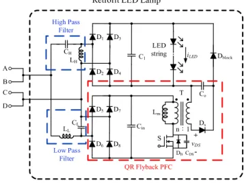
Therefore, a novel retrofit LED lamp is proposed as shown in Fig. 1. The driver circuits include high frequency and low frequency paths to drive the LED. The high frequency filter and low frequency filter are used to separate the high frequency input from electronic ballast and the low frequency input from electromagnetic ballast and AC grid, respectively. The low-pass filter is to block the power which is sent from electronic ballasts and allows the power from electromagnetic ballast and AC grid to drive LED. The high-pass filter which allows the power from electronic ballasts to pass is used to block the power from AC grid and magnetic ballasts. A full bridge rectifier is utilized to rectify the power from electronic ballast into DC to drive LED. The connection of the retrofit LED lamp is shorting the double-capped at each side.
II. OPERATING PRINCIPLES OF THE PROPOSED RETROFIT
LEDLAMP
Some assumptions are made in advance to simplify the analysis of the proposed retrofit LED driver.
1) All components are ideal.
2) The turn ratio of the transformer is np/ns = n.
3) Terminal A and B are shorted, and terminal C and D are shorted also.
A. Low frequency input power for retrofit LED lamp
When the proposed retrofit LED lamp is connected to electromagnetic ballast, the starter is needless and has to be removed.
Ds
Co
Dblock
Thus, the equivalent circuit is shown in Fig. 2. The inductor L of electromagnetic ballast and the PFC capacitor CPFC form a π-type low-pass filter with the low-pass filter of the retrofit LED lamp. To simplify the analysis, the π-type low-pass filter can be neglected and the operating principle can be regarded as the system is connected to AC grid input.
The wiring diagram of AC grid input is shown in Fig. 3. The operating principles can be regarded as LED is driven by a flyback converter with quasi-resonant control for PFC.
B. High frequency input power for retrofit LED lamp
Two type ballasts, instant-start and preheat-start electronic ballast, are commonly used the same topology of the class-D inverter which is shown in Fig. 4. The difference between them is the start-up process and will be discussed in the next part.
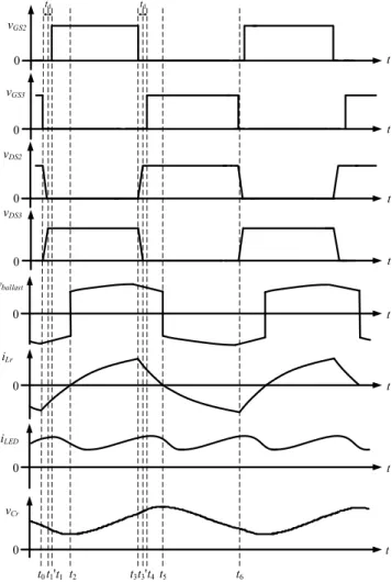
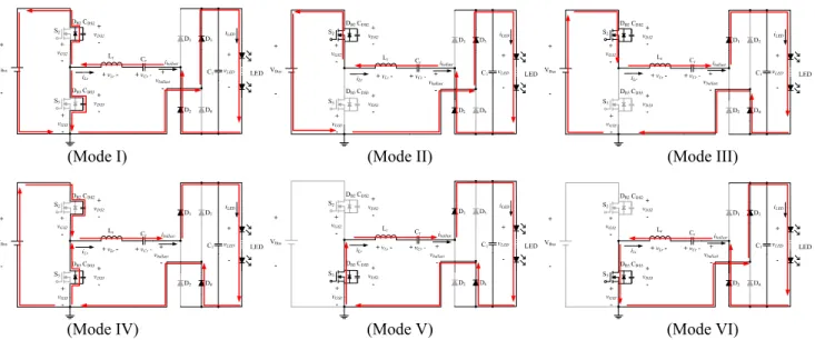
Some assumptions are made before. The operating principles will be focused on the class-D inverter and divided into six modes: mode I to mode VI. The dc bus voltage Vbus is the output of a boost PFC converter typically. Due to the analysis is focus on the steady-state operation after the LED module is turned on, the capacitor Cp which is included in ballast is neglected because of the impedance itself is much bigger than the LED turn-on resistance. The high-pass filter between electronic ballast and full bridge rectifier is also neglected during steady-state analysis. Fig. 5 and Fig. 6 show the key waveforms of the steady state operation and current flowing path when the lamp is driven by electronic ballast, respectively.
Mode 1 [t0 ~ t1 ] :
At t = t0, vGS3 is turned off. iLr goes through parasitic capacitors of MOSFETS CDS2 and CDS3 from t = t0 to t1’. CDS2 is being discharging from VBus to zero while CDS3 is being charging from zero to VBus. Due to the very small value of
CDS2 and CDS3, the crossing voltage of MOSFET vDS2 and vDS2 vary rapidly. From t= t1’ to t1, iLr goes through anti-parallel diode of MOSFETS DB2, making the condition of ZVS for S2. At t = t1, gate signal of S2 becomes high level, this mode ends.
L Ballast Ds Co Dblock vac
Fig. 2 Retrofit LED lamp connect to electromagnetic ballast.
vac
Ds Co
Dblock
Fig. 3 Retrofit LED lamp connect to utility source.
Fig. 4 The equivalent circuit of the proposed LED lamp connected to electronic ballast. 0 0 0 0 0 0 0 t t t t t t t0 t1t2 t3t3' t5 vGS2 vGS3 vDS2 vDS3 iLr vballast vCr t6 0 t iLED t t1' td td t4
Fig. 5 Key waveforms of the proposed LED lamp connected to electronic ballast.
Mode 2 [ t1 ~ t2 ] :
At this mode, vgs2 is turned on at t = t1, but vgs3 is at low level. iLr is negative and making a loop by going through LrS2VBusD3LEDsD2Cr. The output voltage vLED is equal to
-vballast. This mode ends at t = t2 when iLr reaches zero as vCr reaches the minimum.
Mode 3 [ t2 ~ t3 ] :
At this mode, vgs2 is still at high level as vgs3 is still at low level. iLr becomes positive from zero at t = t2 and goes through Lr-Cr-D1-LEDs-D4-VBus-S2. The output voltage vLED is equal to vballast. This mode ends when S2 is turned off at t = t3.
Mode 4 [ t3 ~ t4 ] :
In this interval, vgs2 and vgs3 are at low level, which means both the switches are turned off. S2 is turned off at t = t3, making iLr go through parasitic capacitors of MOSFETS CDS2 and CDS3 from t = t3 to t3’. CDS2 is being charging from zero to VBus while CDS3 is being discharging from VBus to zero. Due to the very small value of CDS2 and CDS3, the crossing voltage of MOSFET vDS2 and vDS2 vary rapidly. From t= t3’ to t4, iLr goes through anti-parallel diode of MOSFETS DB3, making the condition of ZVS for S3.The conduction of LEDs are remained. At t = t4, gate signal of S3 becomes high level, this mode ends.
Mode 5 [ t4 ~ t5 ] :
At this mode, vgs3 is turned on at t = t4, but vgs2 is at low level. iLr is positive and making a loop by going through Lr-Cr-D1-LEDs-D4-S3. The output voltage vLED is equal to vballast. This mode ends at t = t5 when iLr reaches zero as vCr reaches the maximum.
Mode 6 [ t5 ~ t6 ] :
At this mode, vgs3 is still at high level as vgs2 is still at low level. iLr becomes negative from zero at t = t5 and goes through Lr-S3-D3-LEDs-D2-Cr-S2. The output voltage vLED is equal to -vballast. This mode ends when S3 is turned off at t = t6 and the operating backs to Mode 1.
C. Start-up process of electronic ballast
With a different load of fluorescent lamp and LEDs, the sequences of the lamp voltage Vlamp to the switching frequency fS of preheat-start and instant-start have a little difference and as shown in Fig. 7 and Fig. 8, respectively.
Due to the characteristic of fluorescent lamp, the ignition voltage is higher than the steady-state operating voltage. In general, the ignition voltage of a T8 fluorescent lamp using preheat-start is about 200 to 300 V, and over 600 V of using instant-start. Once the voltage is high enough to ionize the gas, the impedance will increase rapidly, and the closed-loop control will dominate the frequency modulation. On the contrary, the turn-on voltage is lower than the steady state operating voltage for LED, the difference between the turn-on voltage and the steady state operating voltage is about from 0.3 V to 1.5 V. Thus, a very high start-up voltage and a low steady state operating voltage will not appear in the case of LED load [10].
III. DESIGN CONSIDERATIONS
This paper proposes a retrofit LED lamp to replace a T8/40W fluorescent lamp been driven by China Electric MFG. Corporation and their key components are shown in Table I and Table II, respectively.
A. LED module design considerations
According to the ANSI standard ANSI-IEC C78.81, the RMS current of the lamp IRMS is about 0.3 ARMS for fluorescent lamp. The average of the lamp current can be derived as following. A 0.27 I π 2 2 dt ) sin( I 2 π 1 I RMS π 0 RMS ave lamp, = = ⋅ ⋅ ⋅ =
θ (1)(Mode I) (Mode II) (Mode III)
(Mode IV) (Mode V) (Mode VI)
The light output of the fluorescent lamp is 2730 lm, the LED is designated at about 22 W with the efficacy of 140 lm/W. Since the current of a 0.2 W LED is 60 mA, 4 strings in parallel operated at 260 mA would be suitable to be driven by fluorescent electronic ballast. Therefore, the number of 112 LEDs is obtained with 28 LEDs in one string .
B. Flyback converter design considerations
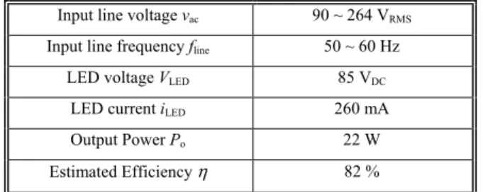
Table III shows the specifications of single stage flyback converter of the proposed LED driver, which is designed for 50/60 Hz universal input voltage range of 90 VRMS to
The output current is a constant of 260 mA and the output voltage is 85 V.
The transformer design affects the overall power efficiency directly due to the switching loss is related to the leakage inductance. The voltage on Lm can be expressed as follows as the switch S is turned on and turned off respectively.
) sin( ) sin( ) sin( ) sin( θ V θ I L t t θ I L θ V V ac peak p, m ON ON peak p, m ac on , Lm ⋅ ⋅ ⋅ = → ⋅ = ⋅ = (2) o peak p, m OFF OFF peak p, m o off , Lm V n θ I L t t θ I L V n V ⋅ ⋅ ⋅ = → ⋅ = ⋅ = ) sin( ) sin( (3)
Where Vac is the amplitude of the input voltage, Ipkp is amplitude of the peak envelope current of the primary side, n is the turn ratio of the primary to secondary windings, and tON and tOFF is the turn on and the turn off time of S, respectively.
The average current of is for half line period is equal to the output LED current ILED and is assumed to be a constant DC value. So that, the relation between the peak envelope current
Ipkp and the output current is described in (4).
LED π 0 s p,peak OFF n I ω dω I T t 2 1 π 1 = ⋅ ⋅ ⋅ ⋅ ⋅ ⋅
sin( t) t (4)Then, the switching frequency can be calculated from (2) and (3), shown in (5). ⋅ + ⋅ = = o ac peak p, m s V n ω V I L T f t) sin( 1 1 1 sw (5)
Eq. (5) shows that the minimum switching frequency fsw,min occurs when the input voltage reaches the peak voltage of the minimum input voltage of 90 VRMS. Therefore, fsw,min can be defined as (6) by substituting π/2 into ωt in (5).
⋅ + ⋅ = 85 1 2 90 1 s n 1 I L f peak p, m min w, (6)
The duty ratio of the switch S can be referred from (2) and (3)
t) sin( 1 1 ω V n V T t D o ac s ON ⋅ ⋅ + = = (7) fpreheat fr1 fr2 fS Strike on
Preheat interval Ignition Steady state
fr1
fr2
Strike on
Ignition Steady state (a) Preheat-start electronic ballast (b) Instant-start electronic ballast Fig. 7 Waveforms of fS v.s. Vlamp with fluorescent lamp.
fSwitch fr1 fr2 fS fO Strike on
Ignition Steady state Lamp voltage fSwitch fpreheat fr1 fr2 fS fO Soft start Strike on
Preheat interval Ignition Steady state Lamp voltage
Fig. 8 Waveforms of fS v.s. Vlamp with LEDs.
TABLEI
SPECIFICATIONS OF THE BALLASTS AND FLUORESCENT LAMP Electromagnetic ballast FG-32115H-L
China Electric MFG. Corporation Electronic ballast FX-40AE-BS8T, Preheat-start
China Electric MFG. Corporation
Fluorescent lamp FL40D
China Electric MFG. Corporation
TABLEII
KEY COMPONENTS OF THE BALLASTS AND FLUORESCENT LAMP Electromagnetic ballast CPFC 8.5 μF L 620 mH Electronic ballast Lr 1.95 mH Cr 120 nF Cp 7.5 nF
Input line voltage vac 90 ~ 264 VRMS Input line frequency fline 50 ~ 60 Hz
LED voltage VLED 85 VDC
LED current iLED 260 mA
Output Power Po 22 W
provide enough discharging time for the Lm. From (7), n is calculated as 2.2 and 2 is selected for the implement to ensure the duty ratio less than 0.6.
From the specifications of the flyback, the input current iac is shown in (8) A 407 0 2 A 288 0 . . = ⋅ = = = rms ac, peak ac, rms ac, o rms ac, I I V η P I (8)
The peak current of magnetizing inductor Ip,peak is described in (9) A 42 1 2 1 . = + ⋅ ⋅ = peak p, OFF ON ON peak p, peak ac, I t t t I I (9)
The current on the secondary side is shown in (10)
A 407 0 2 1 2 1 A 846 2 n . . = + ⋅ ⋅ ⋅ = = ⋅ = OFF ON OFF peak s, rms s, peak p, peak s, t t t I I I I (10)
According to (11), the magnetizing inductor can be gotten
e max p peak p, m I n B A L λ= ⋅ = ⋅ ⋅ (11)
Where maximum magnetic flux density Bmax is set to be 0.35 T, and EI22 is chosen, which the effective area Ae is 33.1 mm2. Therefore, 1mH of the magnetizing inductor is obtained. Finally, the minimum switching frequency fsw,min can be calculated from (6) and is 51.3 kHz.
C. Filters design considerations
The high-pass filter and low-pass filter will highly affect the performance of the retrofit LED lamp. The design of the low-pass filter and the high-low-pass filter will be discussed in detail in the following.
The filter has two functions, one is for blocking high frequency power from the input source, and another is for filtering out the high order harmonic current from the QR flyback to improve the power factor. However, the capacitance will affect the PF when the driver is driven by AC grid. Thus, the corner frequency of the low-pass filter should be under 20 kHz and the relationship with the capacitor and the inductor is shown in (12).
2 1 L L low corner, C L f ⋅ π ≡ (12)
The lower corner frequency is the bigger volume of the core and larger capacitance of CL will be. So, the capacitance should be as small as possible. Therefore, the trade-off between the PF and the size of the inductor results in a selection of 6 kHz as the corner frequency.
The purpose of the high-pass filter is to block the low frequency power of 50 / 60 Hz from AC grid, and allow the high frequency power provided by electronic ballasts to drive LED module. Thus, the corner frequency of high-pass filter is
following. 2 1 H H high corner, C L f ⋅ π ≡ (13)
In order to simplify the analysis, the power factor pf of the flyback in universal range is assumed unity and the efficiency
η is assumed to be 100%. Therefore, the upper limitation
range of the capacitance can be determined to guarantee a PF over 0.9 under the worst case.
nF 400 ≤ eq C (14)
However, the pf in real state will decrease as the input voltage increases and the efficiency η won’t be equal to 100%. Thus, the equation shown in (15) is focused on the situation of 264 VRMS input voltage, where pf and η is set to be 0.97 and 0.82, respectively. 2 H 2 acMax 1 o 2 o o H C ω V (pf) η pf P η P η P ) PF(C ⋅ ⋅ + ⋅ ⋅ + = − cos sin (15)
In order to avoid affecting the performance of electronic ballasts, the filter capacitance has to be as larger as possible and 220 nF is chosen. 6 kHz is selected as the corner frequency of the filter to block the signals under 60 Hz precisely. Thus, the maximum inductance LH can be derived of 3.2 mH and the filter inductor of 3 mH is selected.
Therefore, the filter capacitor CL can be decided to be 150 nF and the filter inductor LL of 5 mH is obtained.
IV. EXPERIMENTAL RESULTS
Table IV shows the key parameters of the proposed retrofit LED lamp. The experimental results will be illustrated in detail in the following.
A. Experiment results of being driven by AC grid
Fig. 9 shows the input voltage vac and input current waveforms iac when the LED driver is driven by AC grid with the input voltage at 110 Vrms and 220 Vrms, respectively. The PFC circuit has an excellent consequent of over 0.998 at the low line input voltage. However, there is a little phase difference between the input voltage vac and input current iac and it becomes larger as the input voltage increases because of the filter capacitor CH and CL.
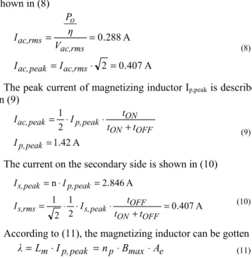
Table V lists the experimental results under universal input voltage range at 60 Hz. The results show that the output current iLED is maintained at 260 mA ± 6 mA under universal input voltage, which shows a good line regulation. The average efficiency is 83.1%.
Fig. 10 shows the power factor of the proposed LED driver at universal input voltage range at 60 Hz. The power factor decreases as the input voltage increases due to the affect by filter capacitors and the lowest power factor is still higher than 0.91 at maximum input voltage.
B. Experiment results of being driven by electromagnetic ballast
Fig. 11 shows the input voltage vac and input current waveforms iac when the LED driver is driven by electromagnetic ballast and the input voltage vac is 110 Vrms. From the figure, the phase difference between the input
voltage vac and input current iac is due to the PFC capacitor which is included in the electromagnetic ballast.
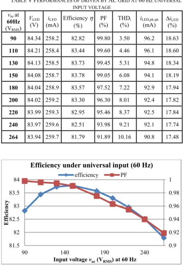
Table VI lists the experimental results when the LED driver is driven by electromagnetic ballast under specific input voltage range at 60 Hz. Table VI (a) shows the results of the entire system which the electromagnetic ballast are included, and Table VI (b) shows the experimental results of the driver.
It can be seen that the PF is mostly affected by the PFC capacitor which is included in the electromagnetic ballast. The loss on the ballast also decreases the overall efficiency. Magnetizing inductor Lm
1 mH EI 22/15/16
NP : NS = 2 : 1 Flyback controller ST L6562D
Flyback switch S IPI60R199CP / 650 V, 10 A Low-pass filter capacitor 150 nF / 400 V Low-pass filter inductor 5 mH LED module 4 strings in parallel / 28 LEDs per string
/ 260 mA rated Filter capacitor
C1 100 nF / 100V
Output capacitor
Co 220 μF / 100V
Flyback diode Ds / 400 V, 1 A UF4004 High-pass filter
capacitor 220 nF / 400 V
High-pass filter
inductor 3 mH
Single LED Rated power: 0.2 W 3 V/ 60 mA
GND(vac , iac) vac:[100 V/div] iac:[100 mA/div] Timebase:[5 ms/div] (a) vac = 110 VRMS / 60 Hz GND(vac , iac) vac:[100 V/div] iac:[100 mA/div] Timebase:[5 ms/div] (b) vac = 220 VRMS / 60 Hz
Fig. 9 Measured retrofit LED lamp input current iac with AC grid driving.
60Hz (VRMS) (V) (mA) (%) (%) (%) (mA) (%) 90 84.34 258.2 82.82 99.80 3.50 96.2 18.63 110 84.21 258.4 83.44 99.60 4.46 96.1 18.60 130 84.13 258.5 83.73 99.45 5.31 94.8 18.34 150 84.08 258.7 83.78 99.05 6.08 94.1 18.19 180 84.04 258.9 83.57 97.52 7.22 92.9 17.94 200 84.02 259.2 83.30 96.30 8.01 92.4 17.82 220 83.99 259.3 82.95 95.46 8.37 92.5 17.84 240 83.97 259.6 82.51 93.98 9.21 92.1 17.74 264 83.94 259.7 81.79 91.89 10.16 90.8 17.48
Fig. 10 Measured retrofit LED lamp power factor and efficiency curves driven by universal AC grid at 60Hz.
0.9 0.92 0.94 0.96 0.98 1 81.5 82 82.5 83 83.5 84 90 140 190 240 Efficiency Input voltage vac(VRMS) at 60 Hz Efficiency under universal input (60 Hz)
efficiency PF
GND(vac , iac)
vac:[100 V/div]
iac:[100 mA/div]
Timebase:[5 ms/div]
Fig. 11 Measured retrofit LED lamp input current iac with electromagnetic ballast driving at vac = 110 VRMS / 60 Hz.
C. Experiment results of being driven by electronic ballast
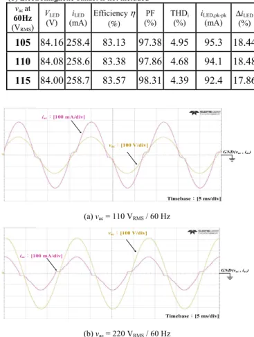
Fig. 12 shows the input voltage vac and input current waveforms iac when the LED driver is driven by electronic ballast and vac is equal to 110 Vrms and 220 Vrms, respectively. The distortion near the zero-crossing section depends on the PFC circuit in electronic ballast.
Fig. 13 (a) shows the waveforms of output voltage vo and output current io of the electronic ballast when the LED driver is driven by electronic ballast at the input voltage vac of 110 Vrms. The resonant of io might be caused by the filters and the resonant tank. However, the LED voltage is regulated by the frequency modulation and the regulation of the LED current is maintained at a good level.
Fig. 13 (b) shows the waveforms of output voltage VLED and output current ILED when the LED driver is driven by electronic ballast at the input voltage vac of 110 Vrms.
(a) Electromagnetic ballast is included
vac at 60Hz (VRMS) VLED (V) iLED (mA) Efficiency η (%) PF (%) THDi (%) iLED,pk-pk (mA) Δi(%) LED
105 84.16 258.4 71.95 70.26 7.15 95.3 18.44
110 84.08 258.6 71.56 64.75 7.64 94.1 18.48
115 84.00 258.7 71.08 60.63 10.47 92.4 17.86
(b) Electromagnetic ballast is not included
vac at 60Hz (VRMS) VLED (V) iLED (mA) Efficiency η (%) PF (%) THDi (%) iLED,pk-pk (mA) Δi(%) LED
105 84.16 258.4 83.13 97.38 4.95 95.3 18.44 110 84.08 258.6 83.38 97.86 4.68 94.1 18.48 115 84.00 258.7 83.57 98.31 4.39 92.4 17.86 GND(vac , iac) vac:[100 V/div] iac:[100 mA/div] Timebase:[5 ms/div] (a) vac = 110 VRMS / 60 Hz GND(vac , iac) vac:[100 V/div] iac:[100 mA/div] Timebase:[5 ms/div] (b) vac = 220 VRMS / 60 Hz
Fig. 12 Measured retrofit LED lamp input current iac with electronic ballast driving. vac at 60Hz (VRMS) VLED (V) iLED (mA) Efficiency η (%) Efficiency ηDriver (%) PF (%) THDi (%) iLED,pk-pk (mA) Δi(%)LED
90 84.64 270.3 84.46 97.37 95.68 9.78 156.7 28.99 110 84.60 270.3 85.27 97.39 97.62 11.23 156.3 28.91 130 84.53 270.2 85.69 97.43 98.44 12.32 156 28.87 150 84.45 270.2 85.88 97.37 98.73 13.22 155.2 28.72 180 84.39 270.1 85.97 97.37 98.75 14.30 155.5 28.79 200 84.37 270.1 85.89 97.40 98.67 14.46 154.6 28.62 220 84.31 270.1 85.73 97.40 98.63 14.48 154.7 28.64 240 84.27 270.1 85.46 97.41 98.51 14.68 154 28.51 264 84.25 270.1 85.04 97.40 97.72 16.53 153.3 28.38 GND(vo) vo:[100 V/div] io:[500 mA/div] GND(io) Timebase:[5 μs/div]
(a) Ballast output vo andio
VLED:[20 V/div]
ILED:[100 mA/div] GND(ILED)
GND(VLED)
Timebase:[5 μs/div]
(b) VLED and ILED
Fig. 13 Measured retrofit LED lamp with electronic ballast driving at vac = 110 Vrms / 60 Hz.
Fig. 14 Measured retrofit LED lamp power factor and efficiency curves with electronic ballast driving vs. universal AC grid at 60 Hz.
0.9 0.92 0.94 0.96 0.98 1 84 84.5 85 85.5 86 86.5 90 140 190 240 Efficiency Input voltage vac(VRMS) at 60 Hz Efficiency under universal input (60 Hz)
97.39 %. The lowest power factor is still higher than 0.95 which occurs at 90 VRMS input voltage. The average efficiency is 85.49% including the ballast.
Fig. 14 shows the power factor of the proposed LED driver driven by the electronic ballast under universal input voltage range at 60 Hz.
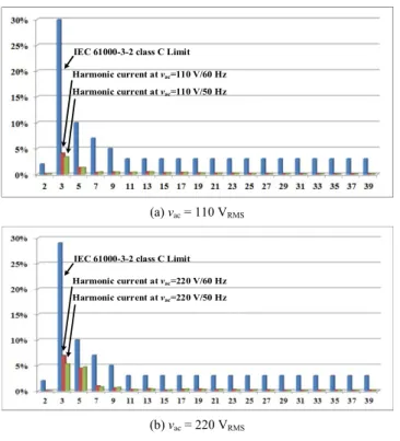
D. IEC 61000-3-2 Standard Compliance
Fig. 15 shows the experiment results when the retrofit LED lamp is driven by AC grid under different input voltage conditions. Fig. 16 shows the results of the LED lamp is driven by electronic ballast under 110 VRMS and 220VRMS input voltage at 60 Hz. The above results are measured by YOKOGAWA WT3000 Precision Power Meter and the embedded standard verification software.
lamp, which is adopted for AC grid, electromagnetic ballast, and electronic ballast. It is a simple solution for replacing fluorescent lamp with LED lamp without modifying the existing lighting fixture and changing any ballast circuitry. The 22 W LED lamp hardware prototype has been designed and implemented for replacing a T8/40 W fluorescent lamp to verify the feasibility of the proposed methods.
VII ACKNOWLEDGEMENT
This work was supported by the Ministry of Science and Technology under Project MOST 104-2218-E-006-028 and 103-2221-E-006 -105 -MY3.
REFERENCES
[1] H. Liu, Y. Yu and X. Liu, “The research of humanized design of the LED landscape lighting lamp,” in Proc. IEEE CAIDCD, pp. 499–502, 2009.
[2] Cree First to Break 300 Lumens-Per-Watt Barrier (March 26, 2014) [on-line]. Available:http://www.cree.com/News-and-Events/Cree-News/Press-Releases/2014/March/300LPW-LED-barrier
[3] J. Y. Tsao, “Solid-state Lighting: Lamps, Chips, and Materials for Tomorrow,” Circuits and Devices Magazine, IEEE, vol. 20, no. 3, pp. 28-37, May/June, 2004.
[4] D. A. Steigerwald, J. C. Bhat, D. Collins, R. M. Fletcher, M. O. Holcomb,M. J. Ludowise, P. S. Martin, and S. L. Rudaz, “Illumination with solid state lighting technology,” IEEE J. Sel. Topics Quant.
Electron.,vol. 8, no. 2, pp. 310–320, Mar./Apr. 2002.
[5] J. Kit, “Retrofit LED lamp for fluorescent fixtures without ballast,” U.S. Patent 7 507 001 B2, Mar. 24, 2009.
[6] J. Robertson and R. Currie, “LED replacement for fluorescent lighting,” U.S. Patent 6 860 628, Mar. 1, 2005.
[7] J. Timmermans, J. Raymond, and J. Ivey, “LED lighting device for replacing fluorescent tubes,” U.S. Patent 7 510 299, Mar. 31, 2009. [8] S. Eiich and H. Kenjiro, “LED Lighting Unit Applied to a Fluorescent
Lighting Fixture,” U.S. Patent Application 2007/0223225, Sep. 27, 2007.
[9] N. Chen and H. Chung, “Driving Technology for Retrofit LED Lamp for Fluorescent Lighting Fixtures With Electronic Ballasts,” IEEE
Trans. Power Electron., vol. 26, no. 2, pp. 588-601, Feb. 2011
[10] H. H. Len, Y. C. Chang, and H. S. Yang, “Driving circuit of compatible LED (Light Emitting Diode) lamp tube,” CN Patent CN 202603010 U, Dec. 12, 2012.
[11] H. H. Len, Y. C. Chang, and H. S. Yang, “New type driving circuit which is compatible with LED lamp tube,” CN Patent CN 202721866 U, Feb. 6, 2013.
[12] H. S. Yang and H. H. Len, “Compatible LED fluorescent tube circuit,” CN Patent CN 203645869 U, Jun. 11, 2014.
IEC 61000-3-2 class C Limit Harmonic current at vac=110 V/60 Hz
Harmonic current at vac=110 V/50 Hz
(a) vac = 110 VRMS
IEC 61000-3-2 class C Limit Harmonic current at vac=220 V/60 Hz
Harmonic current at vac=220 V/50 Hz
(b) vac = 220 VRMS
Fig. 15 IEC 61000-3-2 Class C standard compliance with AC grid driving.
IEC 61000-3-2 class C Limit
Harmonic current at vac=110 V/60 Hz
Harmonic current at vac=220 V/60 Hz
Fig. 16 IEC 61000-3-2 Class C standard compliance with electronic ballast driving.