Influence of polymer gate dielectrics on n-channel conduction
of pentacene-based organic field-effect transistors
Tzung-Fang Guo,a兲Zen-Jay Tsai, and Shi-Yu Chen
Institute of Electro-Optical Science and Engineering, Advanced Optoelectronic Technology Center, National Cheng Kung University, Tainan, Taiwan 701, Republic of China
Ten-Chin Wen
Department of Chemical Engineering, National Cheng Kung University, Tainan, Taiwan 701, Republic of China
Chia-Tin Chung
Chi Mei Optoelectronics Corporation, Tainan Science-Based Industrial Park, Taiwan 741, Republic of China
共Received 6 March 2007; accepted 8 May 2007; published online 22 June 2007兲
This work elucidates the way polymer gate dielectrics affect the accumulation and transport of charge carriers in the active layer of organic field-effect transistors 共OFETs兲. Incorporating a poly共vinyl alcohol兲 polymer interfacial film and another cross-linked poly共4-vinyl phenol兲 layer as a double-layer gate dielectric causes the pentacene-based OFETs to exhibit effective n-channel conduction of a saturated, apparent pinch-off drain-source current with the electron mobility of ⬃0.012 cm2V−1s−1. The formation of an n channel in the pentacene layer is supported by the increased capacitance that is identified by the quasistatic capacitance-voltage measurements of devices with the metal-insulator-semiconductor configuration, biased at a positive gate voltage, in the n-type accumulation regime. © 2007 American Institute of Physics.关DOI:10.1063/1.2748869兴
I. INTRODUCTION
The performance of pentacene-based organic field-effect transistors共OFETs兲 has been steadily improved at field-effect mobilities and on/off current ratios of 0.5– 1 cm2V−1s−1and 106– 108, respectively.1–5
These values are comparable to those of amorphous silicon thin-film transistors. However, most of the OFETs that have been reported to date have a p channel but few have an n channel.6,7 OFETs with high-electron-affinity organic materials as active layers or low-work-function metals as source-drain electrodes exhibit
n-type characteristics under oxygen-free conditions.1,6–11 Re-cently, Chua et al. stated that the trapping of electrons by the hydroxyl groups on the surface of SiO2 gate dielectric layer affected the n-channel conduction of OFETs.12 Most conjugated polymers yield n-type characteristics when a suitable hydroxyl-free polymer, such as a divinyl-tetramethylsiloxane-bis共benzocyclobutene兲 derivative, is used as the gate dielectric. Accordingly, the properties of the interface between the gate dielectric and the organic active layer are critical to the transport and accumulation of posi-tive or negaposi-tive type of charge carriers.
Despite the detrimental effect of the n-channel conduc-tion that has been proposed, Singh et al. observed the ambi-polar characteristics of the pentacene-based OFETs that were fabricated on a poly共vinyl alcohol兲 共PVA兲 gate dielectric.13,14 Notably, 共i兲 pentacene is an organic semiconductor and is frequently used as an active layer for p-type OFETs, but it exhibits both p- and n-type characteristics herein.15–17 共ii兲 PVA is a hydroxyl-group-rich polymer dielectric, which is
considered to interfere with the conduction of electrons for
n-type OFETs, as proposed by Chua et al.12Presumably, the hydroxyl or the polar groups on the PVA dielectric favor the formation of n-channel conduction in the pentacene active layer, and these groups have different functionalities from those on the SiO2 gate dielectric. In this manuscript, a double-layer gate dielectric, incorporating a PVA 共hydroxyl-group-rich兲 polymer interfacial film and a cross-linked poly共4-vinyl phenol兲 共PVP兲 polymer layer, is developed for use in high-performance n-type OFETs. OFETs of pentacene as the active layer with the double-layer gate dielectric ex-hibited very clear n-type output characteristics. They carried a saturated, apparent pinch-off drain-source current with good electron mobility.
II. EXPERIMENT
The basic device configuration herein, presented in the inset in Fig. 1, comprises a prepatterned indium-tin-oxide 共ITO兲/glass 共RITEK Corp., 15 ⍀/䊐兲 gate electrode that is coated with a thin layer of poly共3,4-ethylenedioxythiophene兲:polystyrenesulfonate 共PEDOT:PSS, Bayer Corp. 4083兲, a double-layer gate dielectric 共PVA/ cross-linked PVP兲, a pentacene active layer, and aluminum 共Al兲 source-drain electrodes. The gate dielectric was pre-pared by spin coating 共at 6000 rpm兲 the PVP 共11 wt/ml%兲/poly共melamine-co-formaldehyde兲 methylated 共4 wt/ml%兲 in propylene glycol monomethyl ether acetate 共PGMEA兲 solution18
on a PEDOT:PSS/ITO/glass gate sub-strate. The substrate was baked at 120 ° C for 5 min and then at 200 ° C for 20 min to enable the formation of a cross-linked PVP dielectric layer. Subsequently, the PVA layer was cast on the surface of the PVP layer from 5 wt/ ml% PVA a兲Author to whom correspondence should be addressed; electronic mail:
JOURNAL OF APPLIED PHYSICS 101, 124505共2007兲
0021-8979/2007/101共12兲/124505/4/$23.00 101, 124505-1 © 2007 American Institute of Physics
aqueous solution at 6000 rpm. The substrate was again an-nealed at 65 ° C for 20 min in ambient and another 20 min inside a glove box to eliminate the residual solvent. The thicknesses of PVP and PVA dielectrics are about 270 and 190 nm, respectively, as determined by the capacitance mea-surement. The pentacene 共800 Å兲 active layer and Al 共600 Å兲 source-drain electrodes were deposited sequentially through a shadow mask on the PVA/cross-linked PVP dielectric/PEDOT:PSS/ITO-gate glass substrate inside the vacuum thermal evaporator 共10−6torr兲. The channel length 共L兲 and width 共W兲 of the OFETs in this work are 100 and 1000m, respectively. PVP 共Mw= 20 000兲, PVA 共Mw
= 30 000– 70 000, P8136兲, poly共melamine-co-formaldehyde兲 methylated, PGMEA, and pentacene were purchased from Aldrich and used directly. The current-voltage measurements were made using an HP 4145B semiconductor analyzer. The capacitance-voltage measurements were made using an HP 4284A Precision LCR meter. All of these steps were imple-mented inside a nitrogen-filled glove box, except for the preparation of the PVA/cross-linked PVP dielectric and the PEDOT:PSS/ITO-gate glass substrate.
III. RESULTS AND DISCUSSION
Figure 1 plots the drain-source current versus voltage plots共Idsvs Vds兲 of a pentacene-based OFET that was
fabri-cated on a PVA/cross-linked PVP dielectric/PEDOT:PSS/ ITO-gate glass substrate. When the OFET was operated at a negative gate voltage 共Vg兲 in the p-channel conduction
re-gime, the Ids-Vds plot did not exhibit the output
characteris-tics of a transistor but that of a diode. Although the pentacene-based OFETs of the Au source-drain electrodes exhibited both p- and n-channel conductions on a pure PVA dielectric/ITO-gate glass substrate, which were reported by Singh et al. and also observed in our lab 共not shown here兲, the p-type output was indeed inhibited by the use of the double-layer PVA/cross-linked PVP gate dielectric and the Al source-drain electrodes in this work. Additionally, the Ids
in the diodelike curve, plotted in the Fig.1, declines as Vgis
increased from 0 to − 100 V. This result can be interpreted as indicating that the electron flow, but not the hole flow, contributes substantially to the current. The field-induced positive charge carriers compensated for the conducting elec-trons as Vgwas increased. However, at the current stage, it is
still unclear to comment on the mechanisms resulting in the loss of the p-type output characteristics for pentacene-based OFETs of Al source-drain electrodes that were fabricated on a double-layer PVA/cross-linked PVP gate dielectric. We no-ticed that when only a pure PVA layer was used as the gate dielectric, the leakage current from the ITO-gate electrode was usually at the level around 10−6– 10−7A and was com-parable to Ids. The gate leakage current共Ig兲 has to be
care-fully considered on the influence of the Ids-Vdsmeasurement for OFETs that were fabricated on a pure PVA dielectric/ ITO-gate glass substrate.
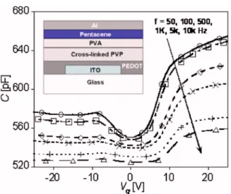
Figure2plots the quasistatic capacitance共C兲 versus the gate voltage 共Vg兲 of the device with the
metal-insulator-semiconductor共MIS兲 configuration. The inset in Fig.2 sche-matically depicts the MIS structure, in which pentacene is deposited onto the double-layer PVA/cross-linked PVP dielectric/PEDOT:PSS/ITO glass substrate and covered by the Al electrode. The C in the C-Vgplot increases slightly at
first to a flat line, when the Vgis biased at a negative voltage
from 0 to − 20 V. The slight increase in C that was measured at the low frequency shows the partial accumulation of the charge carriers in the pentacene layer, but those charge car-riers did not suffice to “open” a p-type channel for conduc-tion. The C-Vg measurements correspond to the
disappear-ance of the transistorlike output characteristics of OFETs, biased at a negative Vgin a p-type accumulation regime.
However, the Ids-Vds plot displays the nice output
char-acteristics of a transistor, as shown in Fig.3, when the OFET device was operated at a positive Vg, in an n-type
accumu-lation regime. The n-type transistor operates with a saturated, apparent pinch-off drain-source current Ids that is close to
1.65⫻10−6A at a Vg of +100 V. In addition, no apparent
hysteresis was seen in the Ids-Vds measurement. The Ids-Vds
features presented in Fig. 3 are seldom observed in n-type
FIG. 2. C vs Vgplots of the device with the MIS configuration measured at
variable frequency共f兲. The inset schematically depicts the MIS structure herein.
FIG. 1. Idsvs Vdsplots of pentacene-based OFET fabricated on the PVA/
cross-linked PVP dielectric, operated at a negative Vg, in the p-channel
conduction regime. The inset shows the basic device configuration of OFETs in this study.
124505-2 Guo et al. J. Appl. Phys. 101, 124505共2007兲
OFETs, especially for pentacene-based transistors. Figure 4 plots the transfer characteristics of Idsvs Vgand共Ids兲1/2vs Vg
plots at a constant Vdsof +100 V. The threshold voltage共Vt兲
and the on-off ratio of the n-type OFET herein are about +40 V and ⬎103, respectively. The electron mobility 共兲 extracted from the saturation region is approximately 0.012 cm2V−1s−1 according to the equation, Ids =共WCi/ 2L兲共Vg− Vt兲2, where Ci共7.5 nF cm−2兲 is the
capaci-tance共measured at 1 MHz兲 per unit area of the double-layer PVA/cross-linked PVP dielectric. Vds did not influence the
gate leakage current共Ig兲 around 10−9 A, which is much less
than Ids.
The formation of an n channel in the pentacene active layer is supported by C-Vgmeasurement. In the right part of
Fig. 2, C increased with Vg from 0 to 20 V, which in fact
probably suggests that the accumulation of electrons at the pentacene active layer is favorable when Vgis in the positive
voltage regime.
The energy barrier to the injection of electrons through the Al electrode to the pentacene layer is high, ⬃1.1 eV. Many attempts have been made to replace the Al source-drain electrodes with Ca or Au. Ids-Vdsmeasurements reveal
that devices with Au electrode have poor n-type output char-acteristics, because the work function of Au is higher than that of Al. Interestingly, devices made of Ca 共a low work function metal兲 source-drain electrodes exhibit no n-type
Ids-Vds characteristics.13 Al is found in our study to be a
better source-drain electrode than Au or Ca for the fabrica-tion of n-type pentacene-based OFETs. Perhaps, the injecfabrica-tion of electrons is retarded by the interfacial reaction between the Ca and pentacene, in which the damaged interface in-creases the barrier height for the injection of electrons.
Chua et al. claimed that the hydroxyl groups on the sur-face of an SiO2 gate dielectric layer interfere with electron transport in pentacene.12 Indeed, observing the n-channel characteristics of typical pentacene-based OFETs fabricated with SiO2as the gate dielectric is difficult. This problem was solved herein by casting a thin PVA layer onto the SiO2 dielectric as a buffer medium. Figure5plots the output char-acteristics of the pentacene-based OFETs that were fabri-cated on the PVA/ SiO2共300 nm兲/n+-Si substrate with Al as the source-drain electrodes. Although the Ids-Vdsoutput plots
are not as good as those in Fig. 3, the OFET exhibits
n-channel characteristics at positive Vg, when an additional
PVA layer is placed on the surface of the SiO2dielectric. The surface morphology of the pentacene layer on the PVA di-electric was characterized by an atomic force microscope, in which the topographical images were similar to the results that had been reported by Singh et al.13The small pentacene crystallines that were observed on PVA dielectric imply a strong interaction at the interface between the pentacene and PVA dielectric during the deposition of the pentacene active layer. The hydroxyl or the polar groups on the PVA polymer chain effectively constitute an appropriate and unique me-dium to stabilize the field-induced and accumulated negative charge carriers close to the contact interface at the pentacene active layer under an electrical bias, where the functionalities differ from those on the SiO2surface as indicated by Chua et
al. The interfacial interaction in the contact interface at
pentacene/PVA dielectric is probably the most critical factor in determining the formation of an effective n-type channel in pentacene-based OFETs.
FIG. 3. Idsvs Vdsplots of pentacene-based OFET fabricated on the PVA/
cross-linked PVP dielectric, operated at a positive Vg, in the n-channel
con-duction regime.
FIG. 4. The transfer characteristics of Idsvs Vgplot and共Ids兲1/2vs Vgplot at
a constant Vdsof +100 V.
FIG. 5. Idsvs Vdsplots of pentacene-based OFET that was fabricated on the
PVA/ SiO2共300 nm兲/n+-Si substrate with Al as the source-drain electrode,
biased at a positive Vg, in the n-channel conduction regime.
124505-3 Guo et al. J. Appl. Phys. 101, 124505共2007兲
IV. CONCLUSIONS
In summary, this study demonstrated the important func-tionalities of polymer gate dielectrics and their effect on the output performance of OFETs. Incorporating a double-layer PVA/cross-linked PVP gate dielectric causes pentacene-based OFETs to exhibit characteristics of n-channel conduc-tion, carrying a saturated, apparent pinch-off drain-source current, a good electron mobility, and a small gate leakage current. The electron mobility extracted from the saturation region is 0.012 cm2V−1s−1, whose value can be increased when the pentacene layer is optimally deposited. The poly-mer dielectric that was directly attached to the pentacene layer governed the transport and accumulation of charge car-riers. The mechanisms by which PVA facilitates the forma-tion of the n channel in the pentacene active layer biased in the accumulation, positive Vg regime are currently being
conducted.
ACKNOWLEDGMENTS
The authors would like to thank the National Science Council共NSC兲 of Taiwan 共NSC95-2113-M-006-002兲 and the Asian Office of Aerospace Research and Development 共AOARD-06-4076兲 for financially supporting this research.
1A. Dodabalapur, H. E. Katz, L. Torsi, and R. C. Haddon, Science 269,
1560共1995兲.
2Z. Bao, A. Dodabalapur, and A. J. Lovinger, Appl. Phys. Lett. 69, 4108
共1996兲.
3Y. Y. Lin, D. J. Gundlach, S. F. Nelson, and T. N. Jackson, IEEE Trans.
Electron Devices 44, 1325共1997兲.
4H. Sirringhaus, T. Kawasem, R. H. Friend, T. Shimoda, M. Inbasekaran,
W. Wu, and E. P. Woo, Science 290, 2123共2000兲.
5M. Stein, J. Mapel, J. B. Benziger, and S. R. Forrest, Appl. Phys. Lett. 81,
268共2002兲.
6J. G. Laquindanum, H. E. Katz, A. Dodabalapur, and A. J. Lovinger, J.
Am. Chem. Soc. 118, 11331共1996兲.
7H. E. Katz, A. J. Lovinger, J. Johnson, C. Kloc, T. Siegrist, W. Li, Y.-Y.
Lin, and A. Dodabalapur, Nature共London兲 404, 478 共2000兲.
8E. J. Meijer, D. M. De Leeuw, S. Setayesh, E. Van Veenendaal, B.-H.
Huisman, P. W. M. Blom, J. C. Hummelen, U. Scherf, and T. M. Klapwijk, Nat. Mater. 2, 678共2003兲.
9T. Yasuda, T. Goto, K. Fujita, and T. Tsutsui, Appl. Phys. Lett. 85, 2098
共2004兲.
10J. Reynaert, D. Cheyns, D. Janssen, R. Müller, V. I. Arkhipov, J. Genoe,
G. Borghs, and P. Heremans, J. Appl. Phys. 97, 114501共2005兲.
11S. Seo, B.-N. Park, and P. G. Evans, Appl. Phys. Lett. 88, 232114共2006兲. 12L.-L. Chua, J. Zaumseil, J.-F. Chang, E. C.-W. Ou, P. K.-H. Ho, H.
Sir-ringhaus, and R. H. Friend, Nature共London兲 434, 194 共2005兲.
13Th. B. Singh, F. Meghdadi, S. Günes, N. Marjanović, G. Horowitz, P.
Lang, S. Bauer, and N. S. Sariciftci, Adv. Mater.共Weinheim, Ger.兲 17, 2315共2005兲.
14Th. B. Singh, N. Marjanović, P. Stadler, M. Auinger, G. J. Matt, S. Günes,
N. S. Sariciftci, R. Schwödiauer, and S. Bauer, J. Appl. Phys. 97, 083714 共2005兲.
15T. Heim, K. Lmimouni, and D. Vuillaume, Nano Lett. 4, 2145共2004兲. 16M. Ahles, R. Schmechel, and H. V. Seggem, Appl. Phys. Lett. 87, 113505
共2005兲.
17Th. B. Singh, P. Senkarabacak, N. S. Sariciftci, A. Tanda, C. Lackner, R.
Hagelauer, and G. Horowitz, Appl. Phys. Lett. 89, 033512共2006兲.
18M. Halik, H. Klauk, U. Zshieschang, G. Schmid, W. Radlik, and W.
We-ber, Adv. Mater.共Weinheim, Ger.兲 14, 1717 共2002兲.
124505-4 Guo et al. J. Appl. Phys. 101, 124505共2007兲