Improved air stability of n -channel organic thin-film transistors with surface
modification on gate dielectrics
Fang-Chung Chen and Cheng-Hsiang Liao
Citation: Applied Physics Letters 93, 103310 (2008); doi: 10.1063/1.2980421
View online: http://dx.doi.org/10.1063/1.2980421
View Table of Contents: http://scitation.aip.org/content/aip/journal/apl/93/10?ver=pdfcov Published by the AIP Publishing
Articles you may be interested in
Analyte chemisorption and sensing on n - and p -channel copper phthalocyanine thin-film transistors J. Chem. Phys. 130, 164703 (2009); 10.1063/1.3078036
Contact resistance and threshold voltage extraction in n -channel organic thin film transistors on plastic substrates
J. Appl. Phys. 105, 084510 (2009); 10.1063/1.3110021
Airstable n channel organic thinfilm transistors with high fieldeffect mobility based on N , N -bis(heptafluorobutyl)-3,4:9,10-perylene diimide
Appl. Phys. Lett. 91, 212107 (2007); 10.1063/1.2803073
Influence of polymer gate dielectrics on n -channel conduction of pentacene-based organic field-effect transistors
J. Appl. Phys. 101, 124505 (2007); 10.1063/1.2748869
High mobility n -channel organic thin-film transistors and complementary inverters J. Appl. Phys. 98, 064502 (2005); 10.1063/1.2043256
This article is copyrighted as indicated in the article. Reuse of AIP content is subject to the terms at: http://scitation.aip.org/termsconditions. Downloaded to IP: 140.113.38.11 On: Wed, 30 Apr 2014 22:54:07
Improved air stability of n-channel organic thin-film transistors
with surface modification on gate dielectrics
Fang-Chung Chena兲and Cheng-Hsiang Liao
Department of Photonics and Display Institute, National Chiao Tung University, Hsinchu 30010, Taiwan
共Received 29 April 2008; accepted 20 August 2008; published online 9 September 2008兲
The air stability of n-channel organic thin film transistors based on N , N
⬘
-dioctyl-3,4,9,10-perylene tetracarboxylic diimide is improved when modifying the dielectric surfaces with polymer insulators. The hydrophobic nature of the polymer surface inhibits protonation of the siloxyl groups on the SiO2surface, leading to fewer SiO−groups that can behave as electron traps. Among the polymerinsulators tested, the devices modified with hydroxyl-free polymers exhibited the best air stabilities. © 2008 American Institute of Physics.关DOI:10.1063/1.2980421兴
Organic thin film transistors 共OTFTs兲 are currently the subject of intensive research owing to their potential appli-cations in low-cost, flexible electronic products, such as flat-panel displays, smart cards, and radio frequency identi-fication tags.1p-channel OTFTs have been prepared that
per-form in a manner comparable with that of amorphous Si;2–4for example, hole mobilities higher than 1 cm2V−1s−1 have been demonstrated for devices based on pentacene.3,4 Although high-performance n-channel devices have also been reported, they function only under inert atmospheres because atmospheric O2 and H2O behave as oxidants and/or
electron traps responsible for n-channel degradation under ambient conditions.1,5–10 One approach toward ambient-stable n-channel OTFTs is the use of organic compounds possessing strong electron-withdrawing units 共e.g., CN groups or F atoms兲 as the semiconducting materials.11–15
The presence of electron-withdrawing side chains increases the electron affinity, stabilizes the charge carriers, and improves the packing of the molecules, thereby preventing the diffu-sion of O2 and H2O into the conducting channel.1Although
this approach is very promising, complicated chemical syn-theses are often necessary. In this study, we substantially improved the air stability of n-channel OTFTs based on
N , N
⬘
-dioctyl-3,4,9,10-perylene tetracarboxylic diimide 共PTCDI-C8兲, which was previously considered16to be an unstable n-channel organic semiconductor in air, by modify-ing the device dielectric surface with insulatmodify-ing polymers 共Fig.1兲. We found that the devices modified with
hydroxyl-free polymers had the best air stability, presumably because of passivation of the siloxyl groups 共electron trapping sites兲 on the SiO2 surface.
Figure 1 illustrates the device structure employed in this study. Heavily n-doped silicon wafers covered with a 200 nm thermally grown SiO2 layer were prepared as
substrates. Polymer solutions were spin coated onto the SiO2 surfaces pretreated with UV ozone under an ambient atmosphere. The polymer dielectric materials studied 共Fig. 1兲 were poly共methyl methacrylate兲 共PMMA兲,
poly-␣-methylstyrene 共P␣MS兲, poly共vinyl alcohol兲 共PVA兲, and poly共4-vinylphenol兲 共PVP兲. PMMA and PS were dissolved in toluene 共1.0 wt %兲, PVA was dissolved in de-ionized water 共2.0 wt %兲, and PVP 共3.0 wt %兲 and
poly共melamine-co-formaldehyde兲 methylated 共1.5 wt %兲, a cross-linking agent, were dissolved in propylene glycol monomethyl ether acetate. The cross-linked PVP films were first baked at 120 ° C for 5 min and then at 200 ° C for 20 min. The other three kinds of polymer films were ther-mally annealed at 100 ° C for 1 h. The thicknesses of the polymer layers were controlled at ⬃70 nm. A semiconduct-ing layer of 50 nm PTCDI-C8 was subsequently deposited at room temperature onto each of the polymer insulators at a base pressure of 3⫻10−6torr. To complete the devices, gold
was deposited under vacuum through a shadow mask to serve as source and drain electrodes. The channel length 共L兲 and width 共W兲 were 90 and 2000m, respectively. The transfer properties of the devices were measured by using Keithley 4200 semiconducting parameter analyzer under am-bient conditions or in a N2-filled glove box. The surface morphology of the PTCDI-C8 films was measured using a Digital Instruments Dimension 3100 atomic force micro-scope 共AFM兲.
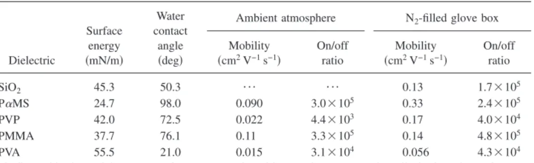
Figure 2 displays the transfer characteristics of the de-vices modified with different polymer insulators under ambi-ent conditions. Each device exhibits typical n-channel behav-ior. Table Ilists the electron mobilities, calculated from the slopes of the plots of the square root of the drain current versus gate voltage in the saturation region. The devices modified with PMMA and P␣MS exhibited higher mobilities and on-off ratios than did the devices modified with the poly-mers containing hydroxyl groups 共PVP and PVA兲.
Further-a兲Author to whom correspondence should be addressed. Electronic mail:
FIG. 1. 共Color online兲 Chemical structures of 共a兲 PTCDI-C8, 共b兲 PMMA, 共c兲 P␣MS,共d兲 PVA, and 共e兲 PVP. 共f兲 Device structure fabricated in this study.
APPLIED PHYSICS LETTERS 93, 103310共2008兲
0003-6951/2008/93共10兲/103310/3/$23.00 93, 103310-1 © 2008 American Institute of Physics
This article is copyrighted as indicated in the article. Reuse of AIP content is subject to the terms at: http://scitation.aip.org/termsconditions. Downloaded to IP: 140.113.38.11 On: Wed, 30 Apr 2014 22:54:07
more, the threshold voltages 共Vth兲 of the devices modified
with PMMA共10.72 V兲 and P␣MS共15.01 V兲 were consider-ably lower than those of the devices modified with PVP 共46.31 V兲 and PVA 共20.22 V兲. Because a higher density of electron traps on a dielectric surface usually leads to an in-creased threshold voltage, our results indicate that the hy-droxyl groups of the buffer polymers must somehow induce the formation of electron traps. On the other hand, the com-plete absence of hydroxyl groups 共electron traps兲 on the P␣MS and PMMA surfaces led to enhanced n-channel con-duction.
Figure3reveals the stability of the devices under ambi-ent conditions. The relative humidity during the period of measurement was controlled at 50%–55%. The devices modified with PMMA and P␣MS exhibited better air stabil-ity than did the bare-SiO2 device and those modified with PVP and PVA. For example, the electron mobility and on/off ratio of the device incorporating PMMA as the modifying layer remained almost unchanged for the first 15 days. The mobility did drop, however, to 0.05 cm2V−1s−1 after
29 days, and eventually to 0.03 cm2V−1s−1after 60 days. In
contrast, when the dielectric buffer layer was PVP or PVA, the electronic mobility and on/off ratio both dropped rapidly. The PVA and PVP devices exhibited poorer n-channel air stability than did the PMMA and P␣MS devices. Indeed, after 20 days, we could not observe any apparent field effect. The morphology of the PTCDI-C8 films deposited on different polymer dielectric layers was examined by AFM 共Fig. 4兲. All the surfaces showed typical rodlike grains.17
Although the grain size of PTCDI-C8 on PVP was slightly different from those of the other three cases, very little
dif-ference were observed between the PTCDI-C8 films on PMMA, P␣MS, and PVA surfaces. Thus, there is no apparent correlation between the morphology and the device perfor-mance measured under ambient conditions.
Previous studies have indicated that charge transport oc-curs only in the first few monolayers of molecules on a di-electric surface.18 Therefore, we deposited only 7-nm-thick layers of PTCDI-C8 on the various dielectric surfaces. The insets of Fig.4display the corresponding morphologies. The grain size of PTCDI-C8 deposited on PVA was smaller than those of the other systems; indeed, the other PTCDI-C8 films, including the one deposited on bare SiO2关inset to Fig.
4共e兲兴, had similar morphologies. These observations are
con-sistent with the performances of the device measured in a N2-filled glove box 共Table I兲, where the PVA-based device
exhibited the lowest mobility. Because smaller grains result in a higher density of grain boundaries, the electron transport was disrupted by the traps located between the grains. Fur-ther, contact angle measurements 共TableI兲 revealed that the
PVA film possessed a very high surface energy, which inhib-ited the growth of ordered PTCDI-C8 crystals. In contrast, the low surface energy of the P␣MS film presumably led to preferential crystal orientation of PTCDI-C8 for effective FIG. 2. 共a兲 Plots of the square root of the drain current vs the gate voltage.
共b兲 Transfer characteristics of the devices modified with the various polymer dielectric materials. The curves were all recorded under ambient conditions.
TABLE I. Characteristics of PTCDI-C8 OTFTs modified with various polymer dielectrics, measured both in a N2-filled glove box and under ambient conditions, in comparison with the results of contact angle
measure-ments. Dielectric Surface energy 共mN/m兲 Water contact angle 共deg兲
Ambient atmosphere N2-filled glove box
Mobility 共cm2V−1s−1兲 On/off ratio Mobility 共cm2V−1s−1兲 On/off ratio SiO2 45.3 50.3 ¯ ¯ 0.13 1.7⫻105 P␣MS 24.7 98.0 0.090 3.0⫻105 0.33 2.4⫻105 PVP 42.0 72.5 0.022 4.4⫻103 0.17 4.0⫻104 PMMA 37.7 76.1 0.11 3.3⫻105 0.14 4.8⫻105 PVA 55.5 21.0 0.015 3.1⫻104 0.056 4.3⫻104
FIG. 3.共Color online兲 Air-stability measurements of PTCDI-C8 OTFTs. 共a兲 Electron mobilities and relative humidity as a function of time.共b兲 On/off ratios plotted as a function of time. Between each measurement, the devices were storied in a cabinet, in which the relative humidity was also controlled at 50%–55%.
103310-2 F.-C. Chen and C.-H. Liao Appl. Phys. Lett. 93, 103310共2008兲
This article is copyrighted as indicated in the article. Reuse of AIP content is subject to the terms at: http://scitation.aip.org/termsconditions. Downloaded to IP: 140.113.38.11 On: Wed, 30 Apr 2014 22:54:07
electron transportation, thereby leading to higher electron mobility under the inert environment.
Whereas the device performances under inert conditions were related to the surface morphology PTCDI-C8 films and the surface energy of the dielectric layer, the electrical prop-erties under ambient conditions were more sensitive to the water and moisture affinities. TableI lists the water contact angles of various dielectric surfaces. The P␣MS and PMMA surfaces were rather hydrophobic, suggesting that their im-proved air stability was probably associated with their mois-ture affinities共Fig.3兲. From a recent study of the influence of
H2O and O2 on the performance of OTFTs, Kumaki et al.
concluded that the adsorption of H2O resulted in deprotona-tion of siloxyl groups 共SiOH兲 to form electron trapping groups 共SiO−兲, in contrast, the deprotonation of SiOH with O2 must involve an electron transfer reaction.19For our
sys-tems, we observed clear n-channel field-effect behavior when using SiO2as the dielectric surface and measuring the
device performance under inert conditions 共Table I兲. This
result differs from the disappearance of the n-channel behav-ior of an untreated SiO2surface, as observed by Chua et al.,6
which probably arose due to the rather low sensitivity to the charging of silanol groups of PTCDI derivatives. In contrast, we observed no field effect when the device was measured in air. Therefore, we infer that the polymers probably inhibited the approach of H2O molecules to the conducting channel.
The hydrophobicity of the polymers, relative to that of the SiO2 surface, limits the absorption of humidity, thereby re-tarding the degradation of the n-channel behavior under am-bient conditions. For the devices incorporating PVP and PVA, the polymers were not only more hydrophobic than
SiO2, but their hydroxyl groups were probably less acidic, leading to less of a tendency to undergo deprotonation with H2O.20 Therefore, the PVP- and PVA-based devices
exhib-ited higher air-stability than did the device fabricated on the bare SiO2surface.
In conclusion, we have found that the modification of SiO2 surfaces using hydroxyl-free polymer insulators, such as PMMA and P␣MS, can improve the air stability of
n-channel OTFTs. We attribute this behavior to passivation
of the siloxyl groups 共electron trapping sites兲 on the SiO2
surface. The results presented here are significant because no complicated chemical synthesis of n-channel organic materi-als with strong electron withdrawing groups is required to prepare these OTFT devices. Finally, our preliminary result indicates that this method could be used for other n-channel semiconductors, such as C60, suggesting that the phenomena
reported here are quite general for n-channel OTFTs.
We thank AU Optronics Corp.共AUO兲 for financial sup-port. This study was also partially supported by the National Science Council共NSC 96-2218-E-009-009 and 96–2112–M-009–011兲 and the Ministry of Education ATU Program 共97W807兲.
1J. Zaumseil and H. Sirringhaus, Chem. Rev. 共Washington, D.C.兲 107,
1296共2007兲.
2A. Facchetti, M. H. Yoon, and T. J. Marks,Adv. Mater.共Weinheim, Ger.兲
17, 1705共2005兲.
3H. Klauk, M. Halik, U. Zachieschang, G. Schmid, W. Radlik, and W.
Weber,J. Appl. Phys. 92, 5259共2002兲.
4Y. Y. Lin, D. J. Gundlach, S. F. Nelson, and T. N. Jackson,IEEE Electron
Device Lett. 18, 606共1997兲.
5Z. Bao,Adv. Mater.共Weinheim, Ger.兲 12, 227共2000兲.
6L. L. Chua, J. Zaumseil, J. F. Chang, E. C. W. Ou, P. K. H. Ho, H.
Sirringhaus, and R. H. Friend,Nature共London兲 434, 194共2005兲.
7S. Tatemichi, M. Ichikawa, T. Koyama, and Y. Taniguchi, Appl. Phys.
Lett. 89, 112108共2006兲.
8Y. Hosoi and Y. Furukawa, Mol. Cryst. Liq. Cryst. 462, 37共2007兲. 9D. Kumaki, S. Ando, S. Shimono, Y. Yamashita, T. Umeda, and S. Tokito,
Appl. Phys. Lett. 90, 053506共2007兲.
10T. D. Anthopoulos, B. Sigh, N. Marjanovic, N. S. Sariciftci, A. M. Ramil,
H. Sitter, M. Cölle, and D. M. de Leeuw,Appl. Phys. Lett. 89, 213504 共2006兲.
11Z. Bao, A. J. Lovinger, and J. Brown,J. Am. Chem. Soc. 120, 207共1998兲. 12H. E. Katz, A. J. Lovinger, J. Johnson, C. Kloc, T. Siegrist, W. Li, Y. Y.
Lin, and A. Dodabalapur,Nature共London兲 404, 478共2000兲.
13C. R. Newman, C. D. Frisbie, D. A. da S. Filho, J. Brédas, P. C. Ewbamk,
and K. R. Mann,Chem. Mater. 16, 4436共2004兲.
14B. Yoo, T. Jung, D. Basu, A. Dodabalapur, B. A. Jones, A. Facchetti, M.
R. Wasielewski, and T. J. Marks,Appl. Phys. Lett. 88, 082104共2006兲.
15R. Schmidt, M. M. Ling, J. H. Oh, M. Winkler, M. Könemann, Z. Bao,
and F. Würthner,Adv. Mater.共Weinheim, Ger.兲 19, 3692共2007兲.
16Y. Hosoi, D. Tsunami, H. Ishii, and Y. Furukawa, Chem. Phys. Lett. 436,
139共2007兲.
17B. A. Jones, A. Facchetti, M. R. Wasielewski, and T. J. Marks, J. Am.
Chem. Soc. 129, 15259共2007兲.
18G. Horowitz,J. Mater. Res. 19, 1946共2004兲.
19D. Kumaki, T. Umeda, and S. Tokito, Appl. Phys. Lett. 92, 093309
共2008兲.
20M. H. Yoon, C. Kim, A. Facchetti, and T. J. Marks,J. Am. Chem. Soc.
128, 12851共2006兲. FIG. 4. 共Color online兲 The morphological images 共3⫻3m2兲 of 50 nm
PTCDI-C8 thin films on various polymer dielectrics surfaces:共a兲 PMMA, 共b兲 P␣MS,共c兲 PVA, and 共d兲 cross-linked PVP. Insets: 1.5⫻1.5m2AFM
images of 7 nm PTCDI-C8 thin films deposited on the corresponding polymer dielectric surfaces. 共e兲 AFM image of the 7 nm PTCDI-C8 thin film deposited on the native SiO2surface. The color scale on the top-right represents the 3⫻3m2 AFM images; that in 共e兲 represents the 1.5
⫻1.5m2images.
103310-3 F.-C. Chen and C.-H. Liao Appl. Phys. Lett. 93, 103310共2008兲
This article is copyrighted as indicated in the article. Reuse of AIP content is subject to the terms at: http://scitation.aip.org/termsconditions. Downloaded to IP: 140.113.38.11 On: Wed, 30 Apr 2014 22:54:07