Abstract—In this paper, a novel band-notched ultrawideband
(UWB) monopole antenna with high notch-band-edge selectivity is proposed and demonstrated. The proposed antenna consists of a radiation patch and an embedded second-order bandstop filter. Using the same substrate area as a fundamental UWB antenna, a bandstop filter composed of a nonuniform short-circuited stub and coupled open-/short-circuited stub resonators, is designed into the fundamental antenna. A detail design procedure for the pro-posed antenna with a second-order maximally flat bandstop filter at 5.5 GHz is presented. As compared to the fundamental antenna, the proposed UWB antenna provides good notch-band suppres-sion from 5.15 to 5.95 GHz, in which the normalized total radiated powers in the notch band are lower than 12 dB. Also, the pro-posed structure provides high band-edge selectivity and flat return loss in the notch band. The measured results, including the return loss and total radiated power, agree with the designed ones.
Index Terms—Band-notched antennas, bandstop filter,
cou-pled open-/short-circuited stub, nonuniform short-circuited stub, notch-band-edge selectivity, ultrawideband (UWB).
I. INTRODUCTION
S
INCE the U.S. Federal Communications Commission (FCC) has released the 3.1–10.6-GHz bandwidth [1], ultrawideband (UWB) communication systems attract great attention in the wireless world due to their advantages, in-cluding high-speed data rate, low power consumption, high capacity, low cost, and low complexity. These UWB systems for communications are especially applied to home networking systems as a technology of wireless personal area networks. As a key component of UWB communication systems, UWB antennas with the fascinated features, such as wide bandwidth, simple structure, and omnidirectional radiation pattern, have been widely investigated.Among the planar UWB antenna designs in the recent liter-ature, the focus is mainly on the slot and monopole antennas. The advantages of slot antennas include wide bandwidth perfor-mance and low cost in the printed circuit board (PCB) process [2]–[4]. The wideband slot antennas can be realized by utilizing a unique tapered-slot feeding structure [2] or a feeding scheme to generate multiple resonances of close bands [3], [4]. Planar monopole antennas have been found as good candidates for Manuscript received July 22, 2011; revised March 17, 2012; accepted May 04, 2012. Date of publication July 10, 2012; date of current version October 02, 2012. This work was supported by the Ministry of Economic Affairs, Taiwan, under Contract 100-EC-17-A-03-S1-195.
The authors are with the Institute of Communication Engineering, National Chiao Tung University, Hsinchu 30050, Taiwan (e-mail: sjchung@cm.nctu.edu. tw).
Color versions of one or more of the figures in this paper are available online at http://ieeexplore.ieee.org.
Digital Object Identifier 10.1109/TAP.2012.2207327
UWB applications owing to their attractive merits, such as ul-trawide impedance bandwidth, simple structure and ease of fab-rication, and good radiation properties. Typical shapes of these antennas are half-disc [5], circle, ellipse [6], [7], rectangle [8], [9], and binomial curved [10].
In practice, interference is a serious problem for UWB application systems. Despite the approval of the FCC for UWB to operate over 3.1–10.6 GHz, it may be necessary to notch-out portions of the band in order to avoid interference with the ex-isting wireless networking technologies such as IEEE 802.11a in the United States (5.15–5.35 GHz, 5.725–5.825 GHz) and HIPERLAN/2 in Europe (5.15–5.35 GHz, 5.47–5.725 GHz). This is due to the fact that UWB transmitters should not cause any electromagnetic interference to nearby communication system such as the wireless local area network (WLAN) applications, and vice versa. Therefore, UWB antennas with notched characteristics in the WLAN frequency band are re-quired. There are various methods to achieve the band-notched function. The conventional methods are cutting a slot on the patch [11]–[14], inserting a slit on the patch [15]–[17], or embedding a quarter-wavelength tuning stub within a large slot on the patch [18]. Recently, the band-notched UWB antenna have been realized by using a pair of T-shaped stubs inside an ellipse slot cut in the radiation patch [19] or embedding loop or multiple stub resonators in a conventional UWB [20]–[22]. Even though these approaches may have good rejection perfor-mance, the achieved notch bandwidth is usually limited since only one radiation null is designed in most of these researches. Also, the required transition bandwidth between the pass and notch bands is extended, which will thus encroach upon the usable pass band.
In this study, a new band-notched UWB monopole antenna, as shown in Fig. 1, is developed. The antenna is mainly com-posed of a radiation patch with good radiation performance from 3.1 to 10.6 GHz. In order to obtain a uniform rejection per-formance over the whole interference band and to shrink the transition bandwidth, a new second-order bandstop filter struc-ture, which consists of a nonuniform stub resonator and a cou-pled-line resonator, is proposed to embed in the radiation patch. This compact bandstop filter would produce two radiation nulls in the notch band and thus yield high skirt selectivity in the band transition region.
This paper is organized as follows. Section II depicts the con-figuration and equivalent circuit of the proposed UWB antenna. The design of each component in the proposed antenna, as well as the design procedure for the whole structure, is described in Section III. Simulated and measured results are then presented in Section IV. Section V gives the conclusions.
Fig. 1. Geometry of the proposed band-notched UWB monopole antenna. (a) Perspective view. (b) Top view. (c) Middle view. (d) Bottom view. (e) Cross-section view.
II. CONFIGURATION ANDEQUIVALENTCIRCUIT Fig. 1(a) shows the geometry of the proposed UWB antenna, which is a three-layer structure with two FR4 substrates in between. Each substrate has a thickness of 0.4 mm, dielectric
Fig. 2. Equivalent circuit of the proposed band-notched UWB monopole an-tenna around the notch band.
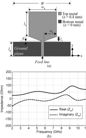
constant of 4.4, and loss tangent of 0.02. Fig. 1(b)–(d) depicts, respectively, the top view, the middle view, and the bottom view of the antenna layout. A signal is to be fed from a 50-microstrip feed line with the signal line on the top layer and the ground plane on the bottom layer. The signal line is connected to a trapezoid patch (with dimensions of ) at point A, as shown in Fig. 1(b). The trapezoid patch is then connected to a pentagon patch on the middle layer through a row of vias [heavy dots in Fig. 1(b) and (c)]. Here, the pentagon patch (with dimensions of ), together with the ground plane on the bottom layer, is the main UWB radiator. Apparently, as illustrated in Fig. 1(e), these two metal patches form a nonuni-form short-circuited stub when looking at the port between points A and C [Fig. 1(c)]. The length of the stub is about a quarter guided wavelength at the center frequency of the notch band. On the bottom layer, two closely spaced strips of different lengths are joined to the ground plane at point B as shown in Fig. 1(d). The shorter strip is connected to the radiation patch on the middle layer through a via. Therefore, when looking at the port between points C and B, one sees a coupled short-circuited stub and open-circuited stub in shunt [Fig. 1(e)]. The lengths of these two stubs are both near a quarter guided wavelength at the notch band. Note that the pentagon patch not only behaves as a radiator but also the ground plane of these stub resonators. The whole antenna size measures 30 mm 27.6 mm, including the ground plane size of 30 mm 10 mm.
Fig. 2 illustrates the equivalent circuit of the proposed an-tenna around the notch band. To realize this circuit, let us start from the feed point A of the antenna. Since the nonuniform short-circuited stub is a quarter-wavelength long, a shunt resonator with resonant frequency at 5.5 GHz appears in between points A and C. Between point C and ground point B, two circuit components are connected in parallel. The first is the coupled stub resonator, which functions as a series resonator , mainly due to the open-circuited stub. And the second is the UWB antenna, formed by the pentagon patch on the middle layer and the ground plane on the bottom layer. Here, since the antenna is to be designed with good performance covering the whole UWB, it is thus modeled as a radiation re-sistance (about 50 ) around the notch band [6].
From the equivalent circuit in Fig. 2, it is obvious that the pro-posed structure has the function of not only an UWB antenna but also a second-order bandstop filter. When a signal of frequency in the notch band enters the structure, it will be reflected back due to the presence of the stub resonators, while as the signal is of other frequency, it will be successfully delivered to the radi-ation patch and radiated out.
monopole antenna is summarized.
A. Fundamental UWB Antenna
Various radiation patch shapes of the planar monopole an-tennas have been studied and utilized to attain the UWB prop-erties. Fig. 3(a) shows the fundamental UWB monopole antenna used in this study. The radiation patch is connected to the 50-microstrip line on the top side of the FR4 substrate with thick-ness of 0.4 mm. The pentagonal shape of the radiator is obtained by trimming the lower edge of a square patch so as to enhance the upper bandwidth. Since a monopole-like UWB antenna at higher frequency usually behaves as a slot antenna [9], properly designing the shape of the bevels on the lower side will cer-tainly improve the excitation of the slot-mode radiation. On the other hand, the current at low frequency is mainly distributed over the patch and the ground plane, which is similar to that of a printed finite-ground monopole antenna. For a given ground plane length , the patch length will determine the lowest operation frequency. The gap between the pentagon patch and the ground plane is also an important parameter, which will in-fluence the impedance matching of the antenna. The final de-sign of the fundamental UWB antenna measures the following
structure dimensions: 14 mm 15.7 mm,
6.24 mm 1.4 mm, 0.5 mm, and 30 mm 10
mm. Fig. 3(b) shows the simulated input impedance by using the full-wave simulation solver High-Frequency Structure Sim-ulator (HFSS) [23]. As expected, the real part of the impedance is near 50 and the imaginary part almost zero, especially in the range from 4 to 7.5 GHz. The input impedance of the an-tenna can be further improved over a wider frequency range by properly shaping the ground plane edge.
B. Nonuniform Short-Circuited Stub Resonator
Since the quality factor of a shunt resonator is propor-tional to ( , where is the parallel resistance of the shunt circuit [24]), to design a shunt resonator with narrow bandwidth, a high-quality factor, and thus a high capac-itance, is needed. Generally, a high-capacitance resonator can be implemented by using a wide short-circuited mi-crostrip stub. However, the large strip width of the resonator may cause transverse resonance, thus destroying the resonator function. The intrusion of the wide strip into the slot region be-tween the radiation patch and the ground plane may also deterio-rate the slot-mode radiation of the antenna. To avoid these prob-lems, here a nonuniform short-circuited microstrip stub, as shown in Fig. 1(b), is utilized. Fig. 4 shows the extracted capaci-tance of this nonuniform stub by using the circuit simulation tool Applied Wave Research (AWR) [25]. By keeping a small strip width ( 2.5 mm) so as not to destroy the radiation slot mode, a short-circuited stub resonator with sufficient
Fig. 3. Fundamental UWB antenna. (a) Configuration. (b) Full-wave simulated input impedance.
Fig. 4. The extracted capacitance of the nonuniform short-circuited mi-crostrip stub resonator as a function of the strip width ( 2.5 mm and
90 at 5.5 GHz).
capacitance can be obtained by choosing a suitable strip width at the short-circuited end.
C. Coupled Open-/Short-Circuited Stub Resonator
To realize the series resonator in Fig. 2, one usually uses a open-circuited microstrip stub. However, this resonant stub shows only a transmission zero at the res-onant frequency, and thus presents low skirt selectivity at the band edges. A open-/short-circuited stub resonator [26], as shown in Fig. 5(a), had been proposed to increase the band-edge selectivity. This circuit behaves as a series resonator at the center frequency due to the open-circuited stub. And at
Fig. 5. The open-/short-circuited stub resonator: (a) conventional type with equal lengths; proposed coupled type (b) with equal lengths and (c) with un-equal lengths. (d) The equivalent series resonator near the center frequency of these stub resonators.
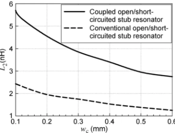
a frequency lower (higher) than the center one, the open-cir-cuited (short-ciropen-cir-cuited) stub shows a capacitive reactance and the short-circuited (open-circuited) stub shows an inductive re-actance, so that the whole circuit behaves as a shunt res-onator. It turns out that the open-/short-circuited stub resonator exhibits a transmission zero at the center frequency and a pair of symmetric transmission poles at the two sides. Nevertheless, due to the low inductance of the series resonator near the center frequency, this stub resonator presents wider notch-band bandwidth [24], which is not suitable for designing a narrow-band narrow-bandstop filter as that in this study. To solve this problem, here we propose a coupled open-/short-circuited stub res-onator, as shown in Fig. 5(b). Moreover, an extended version with different lengths of coupled stubs, as shown in Fig. 5(c), is also introduced. As shown below, this new structure exhibits higher inductance near the center frequency due to the intro-duction of the coupling mechanism, which fits the requirement of the current design. It also has the advantage of producing a pair of asymmetric transmission poles that is contributive to the design flexibility. Besides these good points, the new structure occupies less circuit area due to the close spacing of the two stubs. As the conventional structure, the coupled stub resonator can be equivalent to a series resonator [Fig. 5(d)] near the center frequency.
Fig. 6 shows the extracted equivalent inductance at the center frequency ( 5.5 GHz) of the coupled open-/short-circuited stub, as a function of the strip width that fabricated on a 0.4-mm-thick FR4 substrate by using AWR Microwave Of-fice. The result for the conventional structure is also shown for reference. It is obvious that, for each strip width, the proposed structure gets more than twice the equivalent inductance of the conventional one. Fig. 7 depicts the simulated reflection coef-ficient and transmission coefficient of the coupled stub resonator with different lengths. Here the open-circuited stub has a fixed length 90 (or a quarter wavelength) at 5.5 GHz. The results for different short-circuited stub lengths ( 90 80 70 ) are shown for comparison. It is first ob-served that the response near the center frequency (5.5 GHz) is
Fig. 6. The inductance of the coupled open-/short-circuited stub resonator as a function of the strip width in comparison with the one of the conven-tional structure ( 0.12 mm and 90 at 5.5 GHz).
Fig. 7. Circuit simulation of the coupled open-/short-circuited stub resonator with unequal lengths for different ( 0.5 mm).
unchanged as the stub length decreases from 90 to 70 . This means that the corresponding equivalent circuit (the series resonator) is not influenced by . The structure possesses two transmission poles symmetrically located at 3.3 and 7.5 GHz when the two stubs are with equal length ( 90 ). As the length of short-circuited stub decreases, both transmis-sion poles move to higher frequencies while the transmistransmis-sion zero remains at 5.5 GHz. The frequency shifts for the two trans-mission poles are different. The higher transtrans-mission pole moves faster than the lower one. For designing a bandstop filter, the controlling of transmission poles’ locations is important since they will influence the filter’s out-band (passband) bandwidth and performance. The proposed coupled stub resonator not only possesses high inductance near the center frequency but also provides an extra degree of freedom in controlling the passband characteristics.
D. Synthesis of the Antenna
After designing all the required components as above, one may now integrate them together to synthesize the band-notched UWB antenna by using the following steps.
1) Suitably design the fundamental UWB antenna, as shown in Fig. 3(a), with the bandwidth covering from 3.1 to 10.6 GHz.
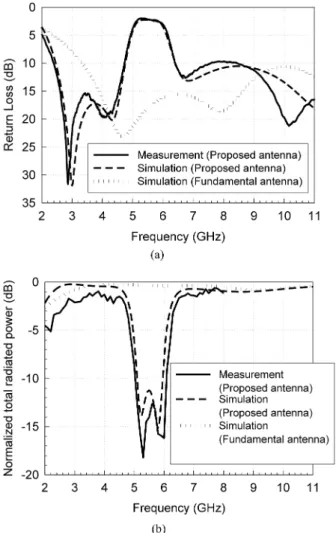
Fig. 8. Simulated and measured results of the proposed UWB monopole an-tenna in comparison with the simulated ones of the fundamental UWB anan-tenna. (a) Return losses. (b) Normalized total radiated powers.
2) Specify the requirements of the bandstop filter to be synthesized, including the operating frequency , the fractional bandwidth , and the type of the filter (e.g., bandstop filter with maximally flat response), from which the circuit elements of a typical bandstop filter in Fig. 2 can be obtained by using the following [24]: (1) (2)
where , and
are the component values of the low-pass prototype filter [24].
3) Using the component values of and obtained above, determine the dimensions of the nonuniform short-cir-cuited stub and the coupled stub resonators with equal stub length according to Figs. 4 and 6, respectively. 4) Properly shorten the short-circuited stub’s length in
the coupled stub resonator so as to adjust the positions of the transmission poles until the bandwidth of the whole UWB antenna is enough.
Fig. 9. Simulated current distributions of the proposed UWB monopole an-tenna at (a) 4 GHz, (b) 5.5 GHz, and (c) 8 GHz.
IV. RESULTS
Following the above design procedures, first, the fundamental UWB monopole antenna is designed with dimensions of
14 mm 15.7 mm, 6.24 mm 1.4 mm, and
0.5 mm. Second, based on the requirement of band notch from 5.0 to 6.0 GHz, the embedded bandstop filter is specified as one with maximally flat response, center frequency 5.5 GHz, fractional bandwidth 18%, and . Here, the maximally flat filter is targeted since it has a 50- load that can be easily realized by a common UWB antenna. (As a note, the second-order Chebyshev filter possesses load impedance near 100 .) Thus, with the specifications and using (1) and (2), the circuit components of the filter can be calculated as 0.37
nH, 2.27 pF, 5.68 nH, and 0.15 pF. Before
going further, it is observed that the single null of the insertion loss at the center frequency of the bandstop filter does not ben-efit the band-edge selectivity. However, from a simple circuit simulation, it is found that the single null can be easily sepa-rated into two (for high band-edge selectivity) by slightly de-creasing the original value of to 5.42 nH, with very limited deterioration in other performances. Then, with the value of and from Fig. 4, the dimensions of the nonuniform short-cir-cuited stub can be decided, which are 2.5 mm, 12 mm, and 8.6 mm. Also, the strip width of the coupled open-/short-circuited stub is determined to be 0.12 mm from
Fig. 10. Measured total-field radiation patterns of the proposed UWB antenna at (a) low-, (b) notch-, and (c) high-frequency bands in the -plane. (Unit: dBi.)
Fig. 6 with the obtained value. (Here the gap between the coupled lines has been chosen as 0.12 mm.) To this step, one now assembles all the components according Fig. 1 to form the band-notched UWB antenna. Finally, to achieve the required an-tenna bandwidth, the electric length of the short-circuited stub is shorten from 90 to 50 by full-wave simulation for the whole structure.
Fig. 8(a) shows the full-wave simulated and measured return loss of the designed UWB antenna. The simulated result of the fundamental UWB antenna without band notch is also shown for reference. The measured return loss of the proposed UWB antenna is in close agreement with the simulated one. It is obvious that the low-frequency band of the proposed UWB antenna is wider than the one of the fundamental UWB antenna due to the existence of the transmission pole at low frequency generated by the coupled stub resonator. Apparently, the embedded bandstop filter in the proposed antenna successfully blocks the input signal from 5 to 6 GHz to radiate. The return loss in this frequency range is quite flat with a value of about 2.5 GHz. Outside this notch band, it rapidly increases to be larger than 10 dB. Good band-edge selectivity is achieved. Note that the nonzero decibel return loss in the notch band is due to the substrate and metal losses produced in the filter resonators. Fig. 8(b) shows the full-wave simulated and measured total radiated powers of the proposed band-notched UWB antenna, together with simulated one of the fundamental UWB antenna. Here, the total radiated power has been normalized to the input power, which is thus equal to the efficiency of the antenna. Note that the total radiated power is measured only from 2 to 8 GHz due to the limited frequency range of the available 3-D
Fig. 11. (a) The proposed UWB antenna with plastic enclosure. (b) Simulated results of return losses and normalized total radiated powers for the proposed antenna with and without enclosure.
radio-frequency (RF) anechoic chamber. It is seen that the sim-ulated result of the proposed UWB antenna has two radiation nulls at 5.25 and 5.8 GHz. As compared to the fundamental UWB antenna, the proposed antenna provides good notch-band suppression from 5 to 6 GHz in which the normalized total radiated power is lower than 10 dB. Also, the proposed struc-ture possesses high notch-band-edge selectivity. The simulated radiation efficiency of the proposed UWB antenna at the fre-quency of 5.5 GHz is only 7.5% and at the two radiation nulls are less than 5%. While outside the notch band, the proposed an-tenna has about the same total radiation power (or anan-tenna effi-ciency) as the fundamental UWB antenna. The measured result of the proposed structure agrees quite well with the simulated one.
Fig. 9 illustrates the simulated current distributions at 4, 5.5, and 8 GHz for the proposed antenna structure. It is seen that at frequencies (4 and 8 GHz) in the passband, more currents are distributed around the radiation patch and the ground plane, which contribute to the radiation of the antenna. On the contrary, the current at the notch frequency (5.5 GHz) is mainly concen-trated on the nonuniform short-circuited stub and the coupled stub resonator. The current on the radiation patch and the ground plane is much weaker, thus resulting in a negligible radiation field as compared to those at frequencies in the passband.
The measured total-field radiation patterns of the proposed UWB antenna at the low, notch, and high-frequency bands in the -plane are depicted, respectively, in Fig. 10(a)–(c). All the radiation patterns are quite omnidirectional. The antenna gains at the low- and high-frequency bands are about 0 dBi, while those at the notch band are below 10 dBi.
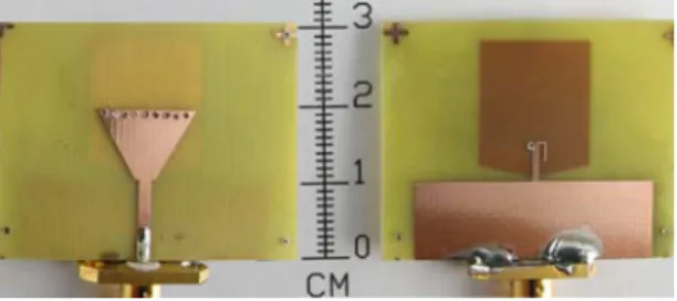
Fig. 12. Photograph of the proposed UWB antenna (left-hand side: top view; right-hand side: bottom view).
In practical application, an antenna is usually put inside a plastic enclosure for mechanical support and waterproofing. To investigate the influence of the enclosure, as illustrated in Fig. 11(a), the designed antenna is inserted into a commonly used enclosure made of 1-mm-thick acrylonitrile butadiene styrene (ABS) with dielectric constant of 2.9 and loss tangent 0.01. The gap between the antenna and the enclosure is set as 2 mm. Fig. 11(b) depicts the simulated results for the antenna with and without the enclosure. It is seen that the normalized total radiated powers for the two cases are almost identical, and the return losses agree well with each other except a little de-terioration from 17 to 13 dB in the passband around 3–4 GHz. The high band-edge selectivity and high and flat normalized radiated power are retained, which implies that the proposed antenna is insensitive to the proximity plastic enclosure.
Fig. 12 shows the photograph of the fabricated band-notched UWB antenna.
V. CONCLUSION
A new UWB monopole antenna with band-notched character-istic in the frequency range from 5 to 6 GHz has been proposed and demonstrated. Occupying about the same substrate area as a conventional UWB antenna, a second-order bandstop filter, re-alized by a nonuniform short-circuited stub and an open-/short-circuited stub resonator, has been designed to merge into the UWB antenna. The measured 10-dB return loss bandwidth cov-ered the range from 2.4 to over 11 GHz with a 3-dB notched band from 5.0 to 6.0 GHz. Good band rejection and notch-band-edge selectivity were achieved. Also, the measured radi-ation patterns of the proposed antenna in the -plane are om-nidirectional, with antenna gains about 0 dBi at frequencies in the passband and below 10 dBi at notch frequencies. Finally, the measured results, including the return loss and total radiated power, showed good agreement with the design ones.
REFERENCES
[1] Federal Communications Commission, “First report and order in the matter of revision of part 15 of the Commission’s Rules Regarding Ultra-Wideband Transmission Systems,” ET-Docket 98-153, Apr. 22, 2002.
[2] T. G. Ma and S. K. Jeng, “Planar miniature tapered-slot-fed annular slot antennas for ultra-wideband radios,” IEEE Trans. Antennas Propag., vol. 53, no. 3, pp. 1194–1202, Mar. 2005.
[3] N. Behdad and K. Sarabandi, “A multiresonant single-element wide-band slot antenna,” IEEE Antennas Wireless Propag. Lett., vol. 3, pp. 5–8, Jan. 2004.
pp. 294–295, Feb. 1998.
[7] L. Jianxin, C. C. Chiau, X. Chen, and C. G. Parini, “Study of a printed circular disc monopole antenna for UWB systems,” IEEE Trans.
An-tennas Propag., vol. 53, no. 11, pp. 3500–3504, Nov. 2005.
[8] M. J. Ammann and Z.-N. Chen, “Wideband monopole antennas for multi-band wireless systems,” IEEE Antennas Propag. Mag., vol. 45, no. 2, pp. 146–150, Apr. 2003.
[9] M. J. Ammann and Z. N. Chen, “A wide-band shorted planar monopole with bevel,” IEEE Trans. Antennas Propag., vol. 51, no. 4, pp. 901–903, Apr. 2003.
[10] C.-W. Ling, W.-H. Lo, R.-H. Yan, and S.-J. Chung, “Planar bino-mial curved monopole antennas for ultrawideband communication,”
IEEE Trans. Antennas Propag., vol. 55, no. 9, pp. 2622–2624, Sep.
2007.
[11] J. N. Lee and J. K. Park, “Impedance characteristics of trapezoidal ultra-wideband antennas with a notch function,” Microw. Opt. Technol.
Lett., vol. 46, no. 5, pp. 503–506, Sep. 2005.
[12] K. L. Wong, Y. W. Chi, C. M. Su, and F. S. Chang, “Band-notched ultra-wideband circular-disk monopole antenna with an arc-shaped slot,” Microw. Opt. Technol. Lett., vol. 45, no. 3, pp. 188–191, May 2005.
[13] C. Y. Huang and W. C. Hsia, “Planar ultra-wideband antenna with a frequency notch characteristic,” Microw. Opt. Technol. Lett., vol. 49, no. 2, pp. 316–320, Feb. 2007.
[14] J. W. Jang and H. Y. Hwang, “An improved band-rejection UWB antenna with resonant patches and a slot,” IEEE Antennas Wireless
Propag. Lett., vol. 8, pp. 299–302, 2009.
[15] H. Yoon, H. Kim, K. Chang, Y. J. Yoon, and Y. H. Kim, “A study on the UWB antenna with band-rejection characteristic,” in
Proc. IEEE Antennas Propag. Soc. Int. Symp., Jun. 2004, vol. 2, pp.
1784–1787.
[16] I. J. Yoon, H. Kim, K. Chang, Y. J. Yoon, and Y. H. Kim, “Ultra wideband tapered slot antenna with band-stop characteristic,” in
Proc. IEEE Antennas Propag. Soc. Int. Symp., Jun. 2004, vol. 2, pp.
1780–1783.
[17] S. Y. Suh, W. L. Stutzman, W. A. Davis, A. E. Waltho, K. W. Skeba, and J. L. Schiffer, “A UWB antenna with a stop-band notch in the 5-GHz WLAN band,” in Proc. IEEE/ACES Int. Conf. Wireless
Commun. Appl. Comput. Electromagn., Apr. 2005, pp. 203–207.
[18] Y. Gao, B. L. Ooi, and A. P. Popov, “Band-notched ultra-wideband ring-monopole antenna,” Microw. Opt. Technol. Lett., vol. 48, no. 1, pp. 125–126, Jan. 2006.
[19] C.-Y. Hong, C.-W. Ling, I.-Y. Tarn, and S.-J. Chung, “Design of a planar ultrawideband antenna with a new band-notch structure,”
IEEE Trans. Antennas Propag., vol. 55, no. 12, pp. 3391–3397, Dec.
2007.
[20] T.-G. Ma, R. C. Hua, and C. F. Chou, “Design of a multi-resonator loaded band-rejected ultrawideband planar monopole antenna with controllable notched bandwidth,” IEEE Trans. Antennas Propag., vol. 56, no. 9, pp. 2875–2883, Sep. 2008.
[21] L.-H. Ye and Q.-X. Chu, “Improved band-notched UWB slot antenna,”
Electron. Lett., vol. 45, no. 25, pp. 1283–1285, Dec. 2009.
[22] S.-J. Wu, C.-H. Kang, K.-H. Chen, and J.-H. Tarng, “Study of an ul-trawideband monopole antenna with a band-notched open-looped res-onator,” IEEE Trans. Antennas Propag., vol. 58, no. 6, pp. 1890–1897, Jun. 2010.
[23] High Frequency Structure Simulator (HFSS). Pittsburgh, PA: Ansoft Corporation, 2001.
[24] D. M. Pozar, Microwave Engineering, 3rd ed. New York: Wiley, 2005, ch. 8.
[25] AWR Microwave Office (MWO). Segundo, CA: AWR Corporation, 2010.
[26] H.-Y. Anita and K.-K. M. Cheng, “Novel dual-band planar resonator and admittance inverter for filter design and applications,” in IEEE
Microw. Theory Tech. Soc. Int. Microw. Symp. Dig., May 2005, pp.
Chao-Tang Chuang was born in Hualien, Taiwan,
on June 2, 1981. He received the B.S. degree in physics from the National Chung Hsing University, Taichung, Taiwan, in 2004, the M.S. degree in electrical engineering from the National Central University, Jungli, Taiwan, in 2006, and the Ph.D. degree in communication engineering from the National Chiao Tung University, Hsinchu, Taiwan, in 2011.
Currently, he is a Senior Engineer with the Advanced Ceramic X Corporation, Ltd., Hsinchu, Taiwan. His research interests include design of microwave circuits, antennas, and low-temperature cofired ceramics (LTCC) passive component for RF applications.
Ting-Ju Lin was born in Ilan, Taiwan. She received
the B.S. degree in communication engineering from the National Chiao Tung University, Hsinchu, Taiwan, in 2010, where she is currently working to-ward the M.S. degree in communication engineering. Her research interests include the design of antennas and multilayer circuit.
Shyh-Jong Chung (M’92–SM’06) was born in
Taipei, Taiwan. He received the B.S.E.E. and Ph.D. degrees from the National Taiwan University, Taipei, Taiwan, in 1984 and 1988, respectively.
Since 1988, he has been with the Department of Communication Engineering and the Department of Electrical Engineering, National Chiao Tung Univer-sity (NCTU), Hsinchu, Taiwan, where he is currently a Professor. He served as the director of the Institute of Communication Engineering, NCTU, from 2009 to 2011. From September 1995 to August 1996, he was a Visiting Scholar with the Department of Electrical Engineering, Texas A&M University, College Station. His areas of interest include the design and applications of active and passive planar antennas, low-temperature cofired ce-ramics (LTCC)-based radio-frequency (RF) components and modules, pack-aging effects of microwave circuits, vehicle collision warning radars, and com-munications in intelligent transportation systems (ITSs).
Dr. Chung received the Outstanding Engineering Professor Award of the Chi-nese Institute of Engineers in 2012, the Outstanding Electrical Engineering Pro-fessor Award of the Chinese Institute of Electrical Engineering in 2006, and the Teaching Excellence Award of National Chiao Tung University in 2005. He served as the Treasurer of the IEEE Taipei Section from 2001 to 2003 and the Chairman of the IEEE Microwave Theory and Techniques Society (MTT-S) Taipei Chapter from 2005 to 2007.