Chapter 4 Design of the fast lock-in amplification scheme for measuring radiation patterns
4.1 System requirements and design consideration
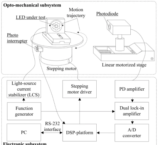
The system requirement is depicted in Fig. 2.1, for measuring the spatial radiance distribution of various light sources (e.g., LEDs) at the rotation resolution of 0.45 degree and in total of three seconds. In this thesis, we propose a real-time lock-in amplification scheme for measuring LED radiation patterns in the presence of ambient light. For the performance evaluation, a Lambertian source is used as a standard specimen to calibrate the proposed system. The proposed system is designed to satisfy the requirements of industry (i.e., fast, high-repeatability, and high-accuracy). Table 4.1 lists the basic specifications of the proposed system.
Table 4.1 The specifications of the fast measurement system Opto-mechanical scheme light-source rotation Horizontal /axial range, theta /
phi
-90° to +90° / -90° to +90°
Minimum angle resolution 0.0025°/Sigma rotary stage 0.45°/ Stepping motor Minimum measurement time @
0.45° measurement interval
3.2 seconds / 180°
Measurement repeatability RMSE is less than 0.003
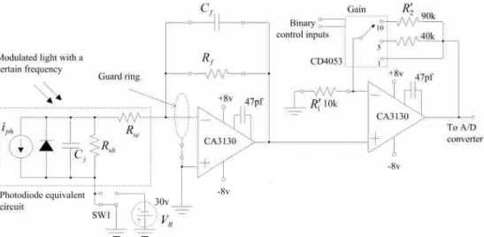
To achieve the system specifications and requirements, this system consists of the electronic and opto-mechanical subsystems, as shown in Fig. 4.1. In the electronic subsystem, the intensity of the LED under test (DUT) is modulated at any specific frequency by the light-source current stabilizer. The light emitted from a DUT is detected by a photoelectric sensor that transforms it into an electric signal. This signal is than amplified by an amplifier and demodulated to recover the original signals by a lock-in amplifier (LIA). The recovered signals
are converted to a digital form by an analog-to-digital (A/D) converter. A microcontroller (i.e., DSP-platform) is applied to pick up and interpret the digital signal. Furthermore, it can transmit the measured data to a PC to display information. In the opto-mechanical subsystem, the DUT is mounted on a rotary stage driven by a stepping motor and microcontroller can perform rotation control through sending control signals to the motor driver.
In the following discussion, the design considerations of the proposed system are studied in detail. Table 4.2 lists the requirements, issues, and proposals of the electronic-circuit design for the fast LED spatial radiance measurement.
Fig. 4.1 System function block diagram
Table 4.2 The requirements, issues, and proposals of the electronic-circuit design for the fast LED spatial radiance pattern measurement [24].
Requirement No. Issue Proposal
1-1
How to enhance the circuit to meet various current specifications of the DUTs and to remove noise in the circuit?
Current
regulation and noise
suppression.
Proper operation and
stabilization for the light sources (or devices under
test, DUTs) (Appendix
A)
1-2 Protection of the DUTs from working at over-rating current?
Over-current protection.
2-1 How to use an op amp to convert a tiny photocurrent to a measurable voltage?
Using an op amp as a TIA.
2-2 How to increase the system stability?
Removing the gain peaking of the PD
amplifier.
2-3
Protection of the photocurrent from the contamination due to the leakage current of the circuit board?
Using the guard ring technique.
Stable, accurate and fast response for the PD
detector.
2-4
Is the performance of a two-stage amplifier better than that of the one-stage PD amplifier, such that the system requirement is met?
Investigating their system stability and bandwidth (or the rise time of a unit-step
response).
3-1
How to reduce the undesired light (or stray light) from external environment (e.g., indoor lighting)?
Using the LIA technique.
3-2 How to increase the bandwidth and stability of the dual LIA?
LPF design considerations (using a high-order Butterworth LPF)
3-3 How to improve the selectivity (or Q values) of the LIA technique?
Using the dual LIA technique.
High-perform ance and fast
response for the LIA
circuit.
3-4
How to reduce the effect of harmonic responses from the LIA technique, and increasing the accuracy of the proposed system?
Using a high Q values BPF to filter out the harmonic signals.
4.2 Design of high-performance optoelectronic sensing device with automatic gain control
In this section, we first review the past and current approaches of optoelectronic sensing techniques (i.e., PD sensing circuit). The performances analysis of those techniques is shown in Appendix B. We compare the advantages and disadvantages of the different structures of the PD amplifier to select a suitable method for the proposed system. To satisfy the fast measurement requirements, the cascade technique of the amplifier is used to increase the bandwidth of the PD sensing circuit. We propose an effective method to perform the PD amplifier. The cascade electronic circuit configuration is that formed by connecting the output of one stage to the input of the one following [25]. In this method, the gain and the bandwidth are increased through cascading a number of stages. From the analyzed results of Type 1 (as show in Appendix B) and the cascade properties, the transfer function of the proposed amplifier can be expressed as
c pf
zf c zf
c fR R S
R R S
S S R
A 2 1
1 2
2 1 1
1
1
, (4.2.1)
where 1R2/R1is the amplification ratio of a non-inverting amplifier based on the op amp.
Obviously, the amplification of this amplifier has been increased by the
1 2 /
1RRfactor. Furthermore, this circuit barely increases a pole point in the transfer function. It appears that the proposed amplifier is more stable than others.
In order to increase the measurement range of the system, the automatic gain control (AGC) unit is designed to change the amplification ratio of the PD sensing circuit that can be used to detect various intensities (i.e., for the low-, meddle-, and extra- brightness LEDs). As shown in Fig. 4.2, the AGC circuit is
installed after the first stage to expand the measurement range of the proposed system.
Fig. 4.2 A schematic for the proposed PD amplifier
4.3 Optical signal processing unit: dual lock-in amplifier
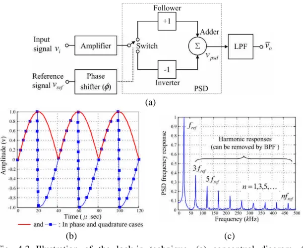
The proposed system is required to perform the measurement under various working environments, such as ambient stray light from other sources in the room. It is difficult to measure the intensity of signals buried in noise (i.e., stray light). The most widely used method of measuring a low level optical signal is to apply a modulation to the light source and then recover the signal at the modulation frequency[25]-[27]. Among the various techniques in use for noise reduction, the lock-in amplifiers are popularly used in combination with modulation techniques to increase the sing-to-noise ratio (SNR) for signals with substantial noise. It can be considered as a band-pass filter with high selectivity (or Q-values).
Figure 4.3(a) shows the basic LIA configuration. It is composed by a phase-sensitive detection (PSD), a phase shifter, and a low-pass filter (LPF). In order to meet the actual requirements, the undesired noise n(t) is considered in
the analysis. Therefore, the input signal vi(t) is composed of a sinusoidal signal
of frequency fs (i.e., modulation frequency) added to the noise. It is expressed as
( ) cos)
(t V t n t
vi s s , (4.3.1)
where 2s fs, and Vs and represent the amplitude and phase of the sinusoidal signal, respectively.
The amplifier amplifies the input signal and then multiplies it by the reference signal vref(t) using the PSD (or called multiplier). The PSD is considered as a
switch which is operated by the reference signal under specific frequency fref. Therefore, the output signal of the PSD can be represented as
harmonicterms(HT) higher frequency terms(HFT).2 cos 1
, 3
3cos cos 1
1 ) ( 3
3cos cos 1
1 cos
) ( ) ( ) (
t V
t t
t n t
t t
V
t rect t v t v
ref s S
ref ref
ref ref
s S
i psd
(4.3.2) where rect(t) is rectangular function which describes the operation of the switch. For simplicity, the phase of the rectangular function is neglected in the analysis process.
If s equalsref, the output of the PSD can be rewritten as HFT HT 2 cos
) 1
( S
psd t V
v . (4.3.3)
As shown in Fig. 4.3(b), the PSD multiplies the input signal by the in phase (0) and in quadrature (/2) components of the reference. If the PSD output passed through a LPF, the HFTs are removed. The filtered PSD output will be represented as
HT 2 cos
) 1
( S
o t V
v . (4.3.4)
The effect of harmonic frequencies (i.e., HTs) on the output of the PSD is shown in Fig. 4.3(c). In order to remove the harmonics of the signal, a band-pass filter (BPF) is used. From analysis result, one can see that the output of LIA and original signals are in direct proportion. In addition, the phase difference between the input and the reference signals decreases the repeatability of the proposed system.
(a)
(b) (c)
Fig. 4.3 Illustration of the lock-in technique. (a) conceptual diagram, (b) switching mixer operation, and (c) frequency response of the PSD.
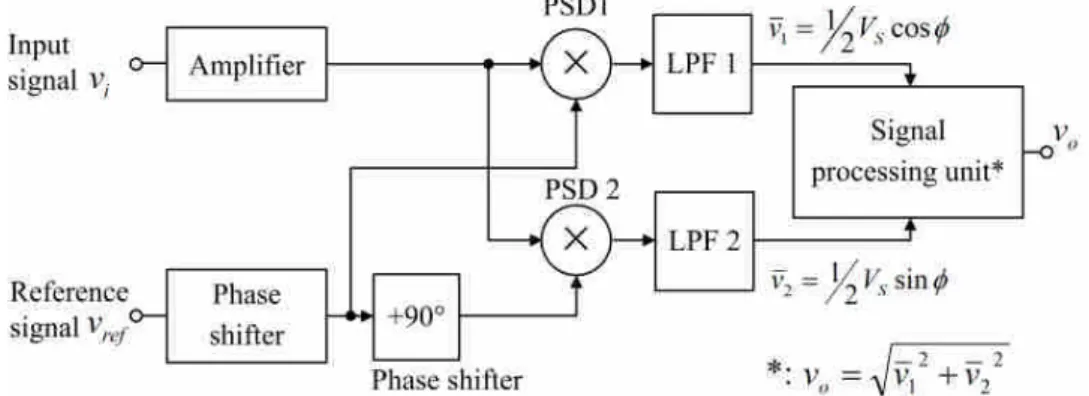
In order to improve the effect of phase difference, we adopt the dual-phase LIA technique to perform our system. As shown in Fig. 4.4, the dual-phase LIA consists of an amplifier, two PSDs, two LPFs, two phase shifters, and a signal processing unit. The phase dependency can be eliminated by adding a second
PSD (i.e., PSD2). If the PSD2 multiplies the signal with the reference signal shifted by 90°, its low-pass filtered output well be
2 sin
) 1
2(t VS
v . (4.3.5)
Thus, the amplitude of the input signal can be computed by the signal processing unit. It can be represented
S
o v t v t V
v 12()22( ) 12 . (4.3.6) Obviously, the output of dual-phase LIA depends on the signal amplitude and unconcerned with the phase between the signal and lock-in reference.
Fig. 4.4 Block diagram of an analog dual phase lock-in amplifier.
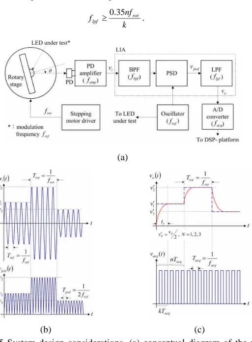
4.4 Design considerations of fast measurement system
In this section, we propose a design method based on system development and implementation considerations to obtain a reliable LIA device in our fast measurement system. The basic block diagram of the proposed system is shown in Fig. 4.5(a). As shown in this figure, we denote the rotation speed of rotary stage as frot. In each motion time step (Trot), the stage rotates an angle (i.e., the minimum resolution of the rotary stage) to change angle () between the DUT and the PD sensor. Therefore, we can measure the intensities of DUT from various angles, and plotting the relative intensity at each angle of radiation
pattern.
In this system, the DUT is modulated with a sinusoidal signal at the frequency of fref which caused it to produce an approximately sinusoidal light intensity output. In order to ensure the detected signal without distortion in measuring process, it is imperative that we determine the bandwidth of each circuit of the proposed system. According to the properties of cascade, the relationship among the bandwidth of PD amplifier (famp), the modulation frequency of DUT, and the central frequency of BPF ( fbpf) are represented as
bpf ref
amp f f
f . (4.4.1)
Thus, the output signals of the PD amplifier (vi(t)) and the PSD (vpsd(t)) are obtained, as shown in Fig. 4.5(b). The output of the PSD is passed through the LPF to remove the AC signals. As shown in Fig. 4.5(c), the response time of the proposed system will be limited by the LPF following the output of the PSD.
According to basic principles of RC-filter circuit, we obtain the relationship between the rise time (tr) of the LPF and its bandwidth ( flpf ). Rise time can be related to bandwidth with the approximation [25]
lpf
r f
t 0.35/ . (4.4.2)
In addition, the system uses the computer-averaging technique to increase the measurement repeatability and accuracy. As shown in Fig. 4.5(c), the voltage data from the LPF are acquired n times by the A/D converter at each rotation interval (Trot). The computer sieves out the usability data from acquired signals, and to average those data. The system removes the unstable signals in rise time
to decrease the measurement uncertainty. In this phase, we assume that the rise time of the LPF is less than kTacq, as shown in Fig. 4.5(c). Thus, we get
lpf r acq
acq kT t f
nT 0.35, (4.4.3)
where nTacq Trot. We calculate the first consideration of design for the fast system from Eq.(4.4.3). It can be represented as
k flpf 0.35nfrot
. (4.4.4)
(a)
(b) (c)
Fig. 4.5 System design considerations. (a) conceptual diagram of the proposed system, and (b)-(c) output signals from the BPF, PSD, and LPF, respectively.
It is well known that the noise is induced from high-frequency signals due to the increase the system bandwidth. To meet the system requirements, we try to increase the noise tolerance of proposed system by decreasing the effective range of the bandwidth of the LPF under the condition of fast measurement (i.e., to satisfy Eq. (4.4.4)). Figure 4.6 displays the frequency response of the LPF. To improve the noise tolerance of the system, the cut-off frequency ( fc) of LPF is set near its 3dB frequency (i.e., bandwidth). In order to achieve this objective, the high-order LPF (e.g., Butterworth LPF) is designed to increase system efficiency.
According to the working principle of the LIA technique as mentioned in Sec.
4.3, the noise tolerance (f ) of the system be represented as
c
ref f
f
f
. (4.4.5)
Therefore, the second consideration of design for the fast system can be expressed
lpf
ref f f
f , f
fnoise max. (4.4.6)To meet the system requirements (i.e., fast and high noise tolerance), the bandwidth of the LPF is designed as
f f
k f nf
ref lpf
rot
35 .
0 . (4.4.7)
Under such conditions, the real-time LIA device is developed to perform the fast LED spatial radiance measurement system.
Fig. 4.6 Design consideration of the LPF for fast measurement system
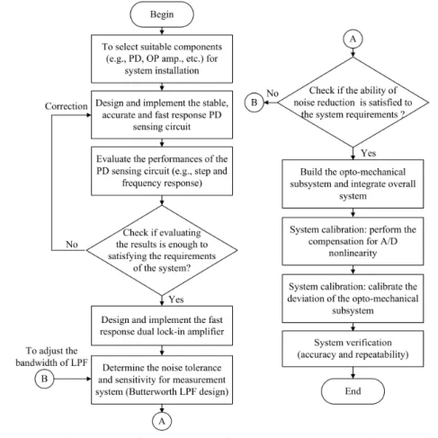
4.5 Experimental procedure for achieving fast measurement system
In this section, a progressive design experiment approach is presented to achieve the fast measurement system. The developing process of the overall system for fast measuring the LED radiance pattern is shown in Fig. 4.7.
Fig. 4.7 Flow diagram of the experimental procedure for achieving fast measurement system
4.6 Evaluating performance of the optoelectronic sensing device
To meet the system requirements, a wideband, stable, and accurate PD amplifier is designed by the progressive method. In the following, the performance of the PD amplifier is evaluated under the various conditions.
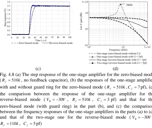
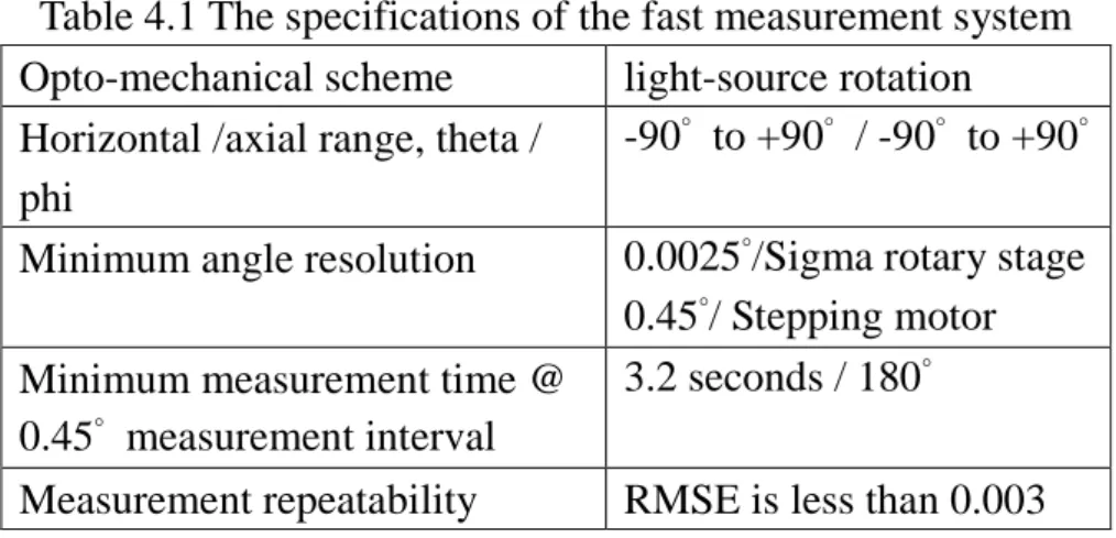
Figure 4.8(a) shows the under-damping (or called gain peaking) of the amplifier in response to the input optical pulse [28]. One can see that the amplifier is under instability that causes serious measurement errors in the system. In order to stabilize the amplifier, the compensation capacitor is used to remove the effect of the gain peaking. Figure 4.8 (b), (c), and (d) show the effectiveness of the reduction for gain peaking in the time and frequency domains, respectively.
In addition, there exists leakage current on the circuit board. To overcome this difficulty, the guard ring technique is used to shield the photocurrent from the leakage current. The effectiveness of this technique is shown in Fig. 4.8(b).
Figure 4.8(c) demonstrates the rise time in revise-biased mode is faster than that in the zero-biased mode. To further increase the amplifier bandwidth, the circuit is improved by adding on more op amp (i.e., AGC unit) to form a two-stage amplifier, as mentioned in Sec. 4.2. Figure 4.8(d) shows a comparison for the system bandwidths of the one-stage and two-stage amplifiers.
0 0.6 1.2 1.8 2.4 3 3.6 4.2 4.8
0 100 200 300 400 500 600 700 800 900 1000
Time(μs)
Amplitude(V)
(a) (b)
(c) (d)
Fig. 4.8 (a) The step response of the one-stage amplifier for the zero-biased mode (Rf 510k, no feedback capacitor), (b) the responses of the one-stage amplifier with and without guard ring for the zero-biased mode (Rf 510k,Cf 7pf), (c) the comparison between the response of the one-stage amplifier for the reverse-biased mode (VB 30V , Rf 510k , Cf 3 pf) and that for the zero-biased mode (with guard ring) in the part (b), and (c) the comparison between the frequency responses of the one-stage amplifiers in the parts (a) to (c) and that of the two-stage one for the reverse-biased mode (VB 30V ,
k
Rf 110 , Cf 5pf)
4.7 Design, perform, and evaluate the dual lock-in amplifier
To improve the SNRs of the proposed system, the dual LIA device is designed to reduce the effects of ambient noise light (or undesired signals). The working principle of the dual LIA has been discussed in Sec. 4.3. Its design diagram is shown in Appendix C.
In the following, we present the experimental results of the dual LIA to verify its performance. Figure 4.9(a) shows the measured signal from the PD amplifier.
One can see that the signal consists of the stray light and the wanted signal from the DUT. Obviously, the signal of the DUT is buried in the stray light that be produced by the indoor lighting devices. In Fig 4.9(b), the experimental result exhibits that the PSDs multiply the input signal by the in quadrature and anti-phase components of the reference. Figure 4.9(c) shows the measurement
results of the output signals of the Butrttworth LPFs. These signals are generated by filtering the output signals of the PSDs in part (b). Thus, the undesired lights are removed through the designed LIA device. Figure 4.9(d) shows the pulse-response of the signal processing unit that processes the mathematical operation ofvo 2vi2 1.414vi (wherevi and vo are the input and output signals of the signal processing unit, respectively).
(a) (b)
(c) (d)
Fig. 4.9 Experimental results for the dual lock-in amplifier. (a)the detected signals, (b) the output signals of the PSDs with demodulation frequency 100kHz, (c) the comparison between the two output signals of the Butterworth LPFs under the conditions of the part (b), and (d) the time-response of the signal processing unit.
4.8 Overall system integration, calibration and verification 4.8.1 Integrating the overall system
The aim of this section is to integrate the LCS, PD amplifier, LIA, and a DSP device (as a microcontroller) into the electronic subsystem. First, we develop the basic DSP hardware/software to control input and output (I/O) devices and communicate with these devices. For example, the opto-mechanical subsystem is driven by a stepping motor that is controlled by the microcontroller. Also, the measurement results are acquired by the microcontroller and they are transmitted to a PC via a RS232 interface. Second, the optoelectronic sensing devices (including PD amplifier, AGC, and LIA, etc.) are connected to the microcontroller with adequate peripherals, such A/D converter. The program of the microcontroller is designed to acquire and transmit the measurement results to a PC, as depicted in Fig. 4.10.
Fig. 4.10 Flow chart of the measurement system
We design a graphic user interface (GUI) to display and manipulate the measurement results, and to communicate with the microcontroller, as shown in Fig. 4.11. In addition, to reduce noise in the optoelectronic sensing process, we employ computer-averaging technique to increase the measurement repeatability and accuracy.
The opto-mechanical subsystem is designed according to the Scheme 1, as mentioned in Sec. 3.2. Subsequently, it is incorporated with the electronic subsystem to form the overall system. Figure 4.12 displays a photograph with the proposed system.
Fig. 4.11 GUI for the system
Fig. 4.12 A photograph of the proposed system
4.8.2 System calibration for A/D non-linearity and other undesired properties
Usually, the response of the optoelectronic sensing circuit (including the PD amplifier and A/D converter) needs to be corrected. This is because the characteristics of PDs are fairly linear in response to the illumination of incident light and thus the measurement errors mainly arise from the nonlinearity of the A/D converter [29]. The use of neutral density (ND) filters (Wratten No. 96, Kodak Inc., USA) with different optical densities is required to characterize the overall response (or the deviation from linearity) of the amplifier and converter.
In the linearity testing phase, we install twelve ND filters on the filter wheel, as shown in Fig. 4.13.The ND filters are used to modulate the light source (i.e., LED) for producing light, incident upon the optoelectronic sensing device, with various luminous levels. Therefore, it is found that the responses of the sensing device to incident light with various intensities are quite linear under different gains of AGC circuit (e.g., G = 1, 2, 5, and 10). In Fig. 4.14, it displays the
experimental results and the correction to the nonlinearity using a linear regression technique.
Fig. 4.13 Schematic diagram of the automatic measurement system for linearity testing
Fig. 4.14 Experimental results of linearity testing for the proposed system with different gain of AGC.
4.8.3 Opto-mechanical subsystem calibration
To calibrate the rotating angle of the opto-mechanical subsystem, a standard light source with Lambertian angular intensity distribution is used to identify the rotating position of the stepping motor (or rotary stage). As shown in Fig. 4.15, it clearly shows that the spatial radiance pattern of the Lambertian source has cosine angular distribution. Hence, the characteristic of the Lambertian source can be used to help the opto-mechanical subsystem calibration.
To evaluate the position error in realizing the set angles of the rotary stage, the Lambertian source is placed on the stage with specific deviation angles (e.g., 15°, 30°, 45°, and 60°, etc.). As the source is rotated along motion trajectory by the rotary stage, the spatial radiance patterns can be measured, as shown in Fig. 4.15.
According to the measurement results, we can evaluate the deviation values of opto-mechanical system. As shown in Table 4.3, the deviation values of opto-mechanical system are less than one degree. One can see that the calibration result is quite satisfactory.
Fig. 4.15 Angle calibration of the opto-mechanical subsystem using a standard light-source
Table 4.3 Measurement results of deviation values for the opto-mechanical system
No. Set values Measurement values Deviation values
1 0 0 0
2 15 14.4 0.6
3 30 29.25 0.75
4 45 45 0
5 60 60.75 0.75
6 75 75.15 0.15
7 90 89.55 0.45
4.9 Evaluation the performance of proposed system
In this section, we briefly compare the measurement results in progressive way.
As a calibrating lamp, a LED (model No. LXHL-LW6C, Lumileds, USA) with a commercially-available acrylic diffuser is used to form an area light source. We test proposed system with such a lamp having the characteristic of Lambertian cosine. As shown in Fig 4.16, it shows the experimental results form the proposed system with the different conditions (e.g., with/without linearity calibration, and with/without LIA device, etc.).
Figure 4.16(a) and (b) display the measured spatial radiation patterns of the calibrating lamp, from the proposed system (without LIA device), with and without external stray light (e.g., indoor lighting fixtures, etc.), respectively. The latter comes from the proposed system under the condition of a dark room. One can see that the noise is still introduced from other undesired sources. To reduce the noise effect, we try to simply make use of the technique of computer averaging (e.g., averaging the measured data), by means of increasing the number of the acquisitions (or measurement times) at each rotation angle. In Fig.
4.16(b), the dash-dotted line shows the 10-times averaged result of the radiation pattern measured from the proposed system without LIA device. Obviously, the
radiation pattern measured from the proposed system with computer averaging is closer to the ideal one of the calibrating lamp than those from the same system without averaging process.
Figure 4.16(c) shows the measured results of the calibrating lamp, from the proposed system with LIA device, under the same condition of Fig. 4.16(a). We can see that the stray light (or undesired noises) can be filtered out by the use of LIA technique. It is worth mentioning that the measured data from optoelectronic sensing device with the compensation for the nonlinearity mainly arising from the A/D converter gives a satisfactory result, as shown in Fig. 4.16(c). Finally, after the system calibration, we can find that the spatial radiance distribution of the calibrating lamp is quite close to the Lambertian cosine law, as mentioned in Sec. 2.1. The measured radiation patterns for the LED with various packages are displayed in Fig. 4.16(c).
(a) (b)
(c) (d)
Fig. 4.16 The measurement results from the system with different conditions, for the calibrating light source and LED under test: (a) the system under external
stray light/noise without LIA, (b) without and with computer averaging (10 times) in the dark, (c) the system with LIA under the same external condition in part (a), and having the compensation for the deviation from linearity, and finally, (d) the system with the part (c), measuring the Lumiled LEDs
For evaluation of system stability, root-mean-square-error (RMSE) is popular method to determine the measurement repeatability of the system. Table 4.4 shows the evaluation results of measurement repeatability in different parts of the proposed system. In this phase, we calculate the repeatability of proposed system based on the RMSE between the measured data and the standard values (i.e., 50-times averaged result). The experimental results indicate that the uncertainty (e.g., undesired noise from print circuit board, and opto-mechanical instability, etc.) of the proposed system can be decreased by increasing the number of the averaging-times. According to the results of evaluation, we can see that the repeatability of the proposed system is satisfactory.
Table 4.4 Repeatability evaluation of the proposed system
No. Item
Root mean squares errors (RMSE) of
measurements*
Sampling rate 1 Electronic device (including PD amp.,
LIA, and A/D converter, etc.) 0.0034527 /
2a
1D fast measurement (using rotary stage (Sigma SGSP-40YAW)/stepping motor)
0.0071234/0.0071323 400/180°
2b
1D fast measurement with computer averaging (5/10 times with respect to 50 times)
0.0034224/0.0027717 400/180°
3 3D fast measurement 0.012259 100/180°
*: Differences of the measured-data averages from the corresponding ones of the 50 times measurements.
![Table 4.2 The requirements, issues, and proposals of the electronic-circuit design for the fast LED spatial radiance pattern measurement [24].](https://thumb-ap.123doks.com/thumbv2/9libinfo/7071770.20014/3.892.118.778.135.1139/requirements-proposals-electronic-circuit-spatial-radiance-pattern-measurement.webp)
![Figure 4.8(a) shows the under-damping (or called gain peaking) of the amplifier in response to the input optical pulse [28]](https://thumb-ap.123doks.com/thumbv2/9libinfo/7071770.20014/13.892.133.757.870.1111/figure-shows-damping-called-peaking-amplifier-response-optical.webp)