Temperature-dependent study of n-ZnO / p-GaN diodes
Kuang-Po Hsueh, Shou-Chien Huang, Ching-Tai Li, and Yue-Ming Hsina兲 Department of Electrical Engineering, National Central University, Jhong-Li 32054, Taiwan Jinn-Kong Sheu and Wei-Chih LaiInstitute of Electro-Optical Science and Engineering, National Cheng Kung University, Tainan 70101, Taiwan
Chun-Ju Tun
National Synchrotron Radiation Research Center, Hsinchu 30076, Taiwan
共Received 17 October 2006; accepted 20 February 2007; published online 28 March 2007兲 This work investigates the temperature dependence of the current-voltage 共I-V兲 characteristics of
n-ZnO / p-GaN junction diodes. The n-ZnO films were deposited on top of the p-GaN by dc
sputtering with subsequent annealings at 500, 600, 700, and 800 ° C for 60 s. The Hall measurement and the x-ray diffraction pattern are measured to study the n-ZnO films. The temperature sensitivity coefficients of the I-V characterizations are obtained by different substrate temperatures 共25, 50, 100, and 150 ° C兲 and the extracted values are 2.10, 1.93, 3.22, and 1.36 mV/ °C in the forward bias and 8.7, 8.0, 4.6, and 2.3 mV/ ° C in the reverse bias, respectively. The fabricated n-ZnO / p-GaN diode with ZnO annealing temperatures at 800 ° C demonstrates the lowest temperature dependence. © 2007 American Institute of Physics.关DOI:10.1063/1.2716324兴
GaN-based materials are the favorable wide-band-gap materials which have been developed on an industrial scale for use in light emitting diodes 共LEDs兲 and high electron mobility transistors. However, relatively less work was re-ported on GaN-based heterojunction bipolar transistors 共HBTs兲 because a good Ohmic contact to p-GaN is difficult to obtain.1–4To avoid the dry etching, several methods have been reported including base or emitter regrowth.5,6 In the emitter-regrowth technique AlGaN was regrown on top of GaN base-collector structure to form an AlGaN / GaN HBT without emitter mesa etching. In this work, n-ZnO is deited onto p-GaN to study a n-ZnO / p-GaN diode for the pos-sibility of the ZnO / GaN HBT. Although p-ZnO / n-GaN LEDs have been reported, but the discussion and analysis are limited to the optical characteristics.7 In this study, n-ZnO films were deposited onto the p-GaN by sputtering with sub-sequent annealings at 500, 600, 700, and 800 ° C for 60 s. The Hall measurement and the x-ray diffraction共XRD兲 are used to characterize the n-ZnO films. The I-V characteriza-tions of n-ZnO / p-GaN diodes are investigated in various substrate temperatures. The temperature sensitivity of the I-V characterizations is discussed and analyzed.
The p-GaN materials used in this study were grown by metal organic chemical vapor deposition on c-face sapphire substrates. A 30-nm-thick GaN nucleation layer was depos-ited onto the sapphire substrate at 550 ° C. The temperature was then raised to 1050 ° C to grow an undoped GaN buffer layer and a 1-m-thick p-type GaN. The activation anneal-ing was carried out at 750 ° C for 20 min in the N2ambient. A sheet resistivity of 3.5⫻104⍀/sq was measured from room temperature Hall measurements. The corresponding bulk carrier concentration of⬃1.9⫻1017cm−3and a mobil-ity of 9.2 cm2V−1s−1were obtained.
The Ohmic contacts on p-GaN were formed by evapo-rating a Ni 共20 nm兲/Au 共20 nm兲 metal stack and subse-quently annealing at 500 ° C for 5 min in oxygen ambient.
After the p-electrode deposition, samples were cleaned and patterned with photoresist. Afterward the n-ZnO films were deposited by dc sputtering method and lifted off. The n-ZnO mesa size is 150⫻150m2. The ZnO samples were then annealed at 500, 600, 700, and 800 ° C for 60 s in a rapid thermal annealing 共RTA兲 system. Finally, Cr 共50 nm兲/Au 共150 nm兲 was deposited on top of the ZnO layer for n-type contact. The inset in Fig.1shows the schematic cross section of a ZnO / GaN diode with n and p electrodes. The I-V data were measured on those n-ZnO / p-GaN junction diodes us-ing parameter analyzer共HP4156C兲.
Table I shows the dependence of carrier concentration, electrical resistivity, and Hall mobility of ZnO films on the annealing temperatures. The as-deposited ZnO film does not show the Hall results due to the high resistivity. However, lower resistivity is observed by increasing annealing
tem-a兲Electronic mail: [email protected]
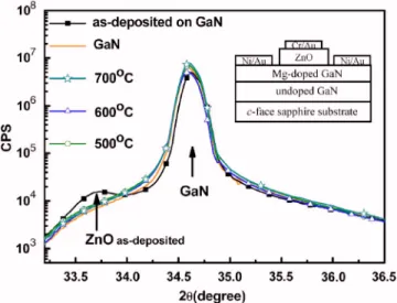
FIG. 1.共Color online兲 XRD patterns of the n-ZnO after annealing in nitro-gen ambient at 500, 600, and 700 ° C for 60 s. The as-deposited ZnO film is also shown. The inset shows the schematic cross section of a ZnO / GaN diode with electrodes.
APPLIED PHYSICS LETTERS 90, 132111共2007兲
0003-6951/2007/90共13兲/132111/3/$23.00 90, 132111-1 © 2007 American Institute of Physics
peratures. The lowest resistivity of 0.016⍀ cm associated with the highest mobility and concentration was obtained after 800 ° C annealing. The experimental results indicate that n-ZnO film with 800 ° C annealing contains more oxy-gen vacancies which play the role of donor. Since oxyoxy-gen vacancies generate states in the band gap and cause an in-crease in conductivity.8
Figure 1 illustrates the x-ray scattering intensity profile of a 2- scan across the 共002兲 reflection of the studied
n-ZnO films using a Bede D1 system. It is shown that the
diffraction angles of the annealed ZnO films remain the same as the GaN without shifting. Although there is a bump at the lower angle from as-deposited ZnO, but it disappeared after annealing. The full width at half maximum of -rocking curves 共not shown兲 decrease with an increase of annealing temperatures, indicating that the crystal quality of the ZnO films could be improved by thermal annealing.
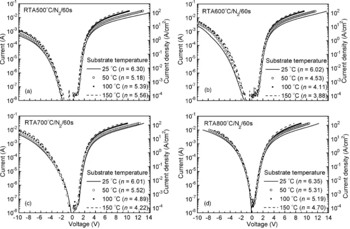
Figures2共a兲–2共d兲show the typical I-V characteristics of the n-ZnO / p-GaN diodes with the ZnO annealing tempera-tures of 500, 600, 700, and 800 ° C, respectively, at different
substrate temperatures. Among four figures, the forward I-V characteristics are similar but reverse I-V characteristics show difference. One can see that the n-ZnO / p-GaN diode with ZnO annealing at 500 ° C demonstrates lowest reverse leakage current. By using theoretical I-V relationship the ide-ality factor is extracted from Fig.2and itemized by the par-enthetic value for each substrate temperature. The extracted ideality factors have the range of 3.88–6.35 and decrease with increasing the substrate temperature. This result could be attributed to the increased concentrations of the n-ZnO layers and lower parasitic resistances existed in the higher substrate temperatures. The ideality factors from the fabri-cated n-ZnO / p-GaN diodes are lower than the published value of⬃8 in room temperature.7The ideality factor of the
n-ZnO / p-GaN diode with ZnO annealing at 800 ° C has the
largest value共6.35兲, but the corresponding turn-on voltage is lowest among all diodes.
The temperature sensitivity coefficient 共␣兲 is analyzed by the equation, V = V0−␣T, where V0is the fitting parameter at T = 0 and V is the bias voltage. Figure3shows the voltages at forward current of 1⫻10−4A as a function of the sub-strate temperatures. The␣values共␣Fin the forward bias兲 of the n-ZnO / p-GaN diodes with ZnO annealings at 500, 600, 700, and 800 ° C are 2.10, 1.93, 3.22, and 1.36 mV/ ° C, re-spectively. The ␣F variation between these n-ZnO / p-GaN diodes is small and their values are comparable with pub-lished results of GaN LEDs.9 Among four diodes, the one with ZnO annealing at 800 ° C demonstrates the lowest tem-perature dependence. However, the ␣F values extracted at higher current共20 mA兲 reveal larger values 共44.4, 36.1, 32.4, and 32.4 mV/ ° C兲 which are attributed to the parasitic
resis-TABLE I. Summary of the Hall measurement on the ZnO samples anneal-ing at different temperatures.
ZnO samples Resistivity 共⍀ cm兲 Mobility 共cm2/ V s兲 Concentration 共1/cm3兲 as-deposited NA NA NA 500 ° C / N2/ 60 s共RTA 500 °C兲 0.2 7 −4.6⫻1018 600 ° C / N2/ 60 s共RTA 600 °C兲 0.14 13 −3.5⫻1018 700 ° C / N2/ 60 s共RTA 700 °C兲 0.033 10 −1.8⫻1019 800 ° C / N2/ 60 s共RTA 800 °C兲 0.016 21 −1.8⫻1019
FIG. 2. Measured I-V characteristics of n-ZnO / p-GaN diodes at different substrate temperatures共25, 50, 100, and 150 °C兲 for the ZnO annealing tempera-tures of共a兲 500, 共b兲 600, 共c兲 700, and 共d兲 800 °C, respectively. The parenthetic value shows the extracted ideality factor.
132111-2 Hsueh et al. Appl. Phys. Lett. 90, 132111共2007兲
tances. The voltages at reverse current of 1⫻10−4A as a function of the substrate temperatures are shown in Fig. 4. The␣ values 共␣R in the reverse bias兲 are 8.7, 8.0, 4.6, and 2.3 mV/ ° C, respectively, for four diodes. The variation of
␣R is larger than ␣F and shows the significant difference in
the reverse characteristic. However, the one with ZnO an-nealing at 800 ° C still demonstrates the lowest temperature dependence.
In summary, the temperature-dependent I-V characteris-tic of n-ZnO / p-GaN junction diodes has been studied. The
n-ZnO films were deposited on top of the p-GaN by dc
sput-tering with subsequent annealings at 500, 600, 700, and 800 ° C for 60 s. The Hall measurement and the XRD inten-sity profile were used to investigate the quality of the n-ZnO films. The temperature dependence of the I-V characteriza-tions is presented for diodes with different ZnO annealing temperatures. The fabricated n-ZnO / p-GaN diodes with ZnO annealing temperatures at 800 ° C demonstrated relative low temperature dependence in forward and reverse biases. This result could be attributed to the lower parasitic resis-tance existed in the 800 ° C annealed samples. Based on the present finding, n-ZnO / p-GaN junction diode is feasible for GaN-based HBTs and p-n junction LEDs.
The authors would like to thank the National Science Council of the Republic of China, Taiwan for financially sup-porting this research under Contract No. NSC 95-2221-E-008-162.
1H. Ishikawa, S. Kobayashi, Y. Koide, S. Yamasaki, S. Nagai, J. Umezaki,
M. Koike, and M. Murakami, J. Appl. Phys. 81, 1315共1997兲.
2J. L. Lee, M. Weber, J. K. Kim, J. W. Lee, Y. J. Park, T. Kim, and K. Lynn,
Appl. Phys. Lett. 74, 2289共1999兲.
3C. B. Vartuli, S. J. Pearton, J. W. Lee, J. Hong, J. D. MacKenzie, C. R.
Abernathy, and R. J. Shul, Appl. Phys. Lett. 69, 1426共1996兲.
4C. C. Kao, H. W. Huang, J. Y. Tsai, C. C. Yu, C. F. Lin, H. C. Kuo, and S.
C. Wang, Mater. Sci. Eng., B 107, 283共2004兲.
5L. S. McCarthy, I. P. Smorchkova, H. Xing, P. Kozodoy, P. Fini, J. Limb,
D. L. Pulfrey, J. S. Speck, M. J. W. Rodwell, S. P. DenBaars, and U. K. Mishra, IEEE Trans. Electron Devices 48, 543共2001兲.
6B. S. Shelton, D. J. H. Lambert, J. J. Huang, M. M. Wong, U. Chowdhury,
T. G. Zhu, H. K. Kwon, Z. L. Weber, M. Benarama, M. Feng, and R. D. Dupuis, IEEE Trans. Electron Devices 48, 490共2001兲.
7D. J. Rogers, F. Hosseini Teherani, A. Yasan, K. Minder, P. Kung, and M.
Razeghi, Appl. Phys. Lett. 88, 141918共2006兲.
8A. Janotti and C. G. Van de Walle, Appl. Phys. Lett. 87, 122102共2005兲. 9Y. Xi and E. F. Schubert, Appl. Phys. Lett. 85, 2163共2004兲.
FIG. 3.共Color online兲 Temperature sensitivity of the I-V characteristics at forward bias.
FIG. 4.共Color online兲 Temperature sensitivity of the I-V characteristics at reverse bias.
132111-3 Hsueh et al. Appl. Phys. Lett. 90, 132111共2007兲