Three TFT Pixel Circuit with Highly stable OLED Current for
AMOLED Displays
Kuan-Wen Chou,
Chia-Che Hung, Fu-Chieh Chang, and Chih-Lung Lin
Department of Electrical Engineering, National Cheng Kung University, Tainan, TaiwanABSTRACT
This work proposes a novel voltage-programming pixel circuit for AMOLED using a-Si:H technology. The proposed 3T1C circuit can stabilize the output current regardless of VTH
shift and OLED degradation. Experimental results indicate that the OLED current degradation is less than 3% over more than 16 h of operation.
1. INTRODUCTION
Owing to lower fabrication cost and better uniformity, hydrogenated amorphous silicon thin-film transistors (a-Si:H TFTs) have been applied to AMOLED displays, which have many advantages, such as a high contrast ratio, a wide viewing range, high response time, and self-emission [1]-[8]. However, a-Si:H TFT is associated with a threshold voltage (VTH) shift
under electrical bias. Since the OLED is a current-driven device, the driving current must be accurately controlled to maintain the uniformity of brightness of displays. Additionally, OLED degradation, which refers to the threshold voltage shift of the OLED and the decay of the emitting efficiency, may result in severe image sticking and a short product lifetime [1], [5]-[8]. In most OLED pixel circuits, the OLED characteristics affect source node of an n-type driving TFT. Therefore, several pixel circuits, such as voltage feedback method [1], [8] and VTH
shift overcompensation method [6], [7], have been proposed to reduce the effect of the VTH shift and improve the OLED
brightness. Nevertheless, these voltage programming methods based on these circuits use an excessive number of TFTs or complicated control signals, resulting in a lower aperture ratio. Therefore, the proposed pixel circuit with only three TFTs can increase the aperture ratio and exploit the VTH shift
overcompensation method to ensure uniformity of brightness. A novel voltage-programming pixel circuit for AMOLEDs is fabricated to elucidate its ability to compensate for VTH
degradation. The proposed pixel circuit, which is composed of three TFTs, can increase the aperture ratio and achieve the brightness uniformity of displays against VTH shifts of TFT and
OLED devices. Measured results demonstrate that the current degradation of the proposed pixel circuit is less than 3%, while that of the conventional pixel circuit is larger than 26% during more than 16 hours of operation.
2. PROPOSED GATE DRIVER CIRCUIT
The a-Si:H TFT was fabricated and the transfer characteristic of TFT under DC bias was measured, as shown in Fig. 1. To investigate the electrical characteristics of the fabricated a-Si:H TFT, experimental results of the drain current flowed from drain node to source node (forward) and from source node to drain node (backward) were shown in Fig. 1(a). As can be seen, the transfer characteristics of the both forward conditions and the backward conditions are similar. Additionally, as shown in Fig. 1(b), the VTH shift of the tested TFT with 500 μm wide and
5.5 μm long is approximately 1.3 V, while the stress condition was in the triode region, with VGS = 20 V, VDS = 0.1 V, and T =
298 K. Therefore, the VTH compensation in the pixel circuit is
essential to stabilizing the driving current in AMOLED display panels.
(a)
(b)
Fig. 1 TFT measurement (a) The width and the length are 100 μm and 5.5 μm, respectively. The voltage of the drain-source node (forward) and source-drain node (backward) is 1 V. (b) Stress-induced changes in the a-Si TFT characteristics at 298 K. The transfer curve of a-Si:H in triode region before and after stress.
Fig. 2 represents the proposed 3T1C pixel circuit and its timing diagram. T1 determines the OLED current by analyzing the storage capacitor voltage of CS, and the other TFTs are used
to perform the switching function. Furthermore, the proposed pixel circuit exploits the inverted OLED structure to eliminate the reduction in current caused by the OLED degradation [8].
The timing diagram, shown in Fig. 2, is divided into three stages – preparation stage, programming stage, and emission stage. In the preparation stage (1), the control signal (SCAN) goes to high voltage (VGH) to turn on T3. Subsequently, the
required data voltage (VDATA) is applied to the gate node (VG)
of T1 and the voltage of node A (VA) is held constant (-VREF).
During the programming stage (2), the reference signal (REF) changes to high voltage and VA starts charging to VSS-VTH2
until T2 is turned off, while VSS is set to zero. The final stage (3)
is the emission stage. SCAN and REF change to low voltage, so that T2 is turned on and T3 is turned off. Notably, based on charge conservation, VG is boosted to VDATA-VREF+VTH2 while
VA is changed from –VTH2 to –VREF. Therefore, the gate-source
voltage of T1 is described as follows.
2 1
_T G SS DATA REF TH
GS V V V V V
V = − = − + (1)
Namely, the OLED current (IOLED) at the emission stage can
expressed as
(
)
(
)
(
)
(3) 2 2 1 2 1 2 1 1 2 2 1 2 1 2 1 2 1 1 _ 1 1 _ TH TH TH TH REF DATA T TH TH REF DATA T TH T GS T T D OLED V V V V V V k V V V V k V V k I I − = Δ Δ + − = − + − = − = =( )
where kT1 is defined as μ⋅Cox⋅
(
W/L)
T1. VTH1 and VTH2indicate the threshold voltages of T1 and T2, whose values are related to the electrical bias stress with time [3]-[10]. The threshold voltage shifts of T1 and T2 can be predicted from the variations of the gate-source voltage and the drain-source voltage with stress time [9], [10]. Thus, IOLED is determined by
VDATA, VREF, and the slight difference between VTH1 and VTH2.
Because T1 and T2 are individually operated in the saturation region and the triode region, VTH2 should be larger than VTH1
under the same gate bias stress [9], [10], such that ΔVTH is
positive and Eq. (2) provides the additional current for OLED device partially to compensate for the degradation in luminance. Consequently, unlike the conventional 2T1C pixel circuit, the proposed driving method, the VTH shift overcompensation
method, can effectively compensate for a VTH shift and achieve
the uniformity of brightness. (a)
(b)
Fig. 2 Proposed pixel circuit and its timing diagram: (1) preparing stage, (2) programming stage, (3) emission stage.
3. RESULTS and DISCUSSION
To investigate the VTH compensation ability of the pixel
circuit, the circuit was simulated using HSPICE, while the simulation model parameters were matched to an a-Si:H TFT model (RPI model level=61). The OLED device was modeled using a widely used diode-connected TFT and parallel capacitor [5]. All TFTs were 5.5µm long and the widths of T1, T2, and T3 were 100µm, 200µm, and 100µm, respectively. Storage capacitor CS was designed with a capacitance of 2pF.
VDD and VSS were 15V and 0V. Additionally, VSCAN and VREF
fluctuated between -20V to 20V and -5V to 5V, respectively. Fig. 3 shows the simulation variation in VA and VG with VTH.
Thus, Fig. 3(a) plots the modulated voltage that is used to charge node A with various VTH deviations in the stage (2).
Differences of the stored voltage in VA are almost identical to
the VTH shifts of T2. Simultaneously, the gate voltage of T1,
shown in Fig. 3(b), can hold the voltage variations to reduce the effect of VTH1 shifts in the emission stage. Therefore, the
proposed pixel circuit can compensate for the variation in the threshold voltage of T1.
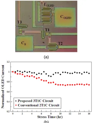
The proposed pixel circuit was fabricated using standard five mask processes. Fig. 4(a) shows the photograph of the fabricated pixel circuit and Fig. 4(b) represents the experimental results obtained using the proposed pixel circuit. To investigate the stability of the OLED current, the required voltage sources are programmed into the test circuit, and the OLED current is measured at the ground node (VSS). Fig. 4(b)
plots the normalized OLED current (IOLED) of the proposed
3T1C circuit after it is stressed for more than 16 h. The OLED current of the conventional 2T1C circuit is also measured for comparison. The normalized OLED current is defined as the measured OLED current divided by the initial OLED current. From the measurement results, the normalized OLED current degradation of the proposed 3T1C pixel circuit is less than 3% of the initial current, while that of the conventional 2T1C pixel circuit is larger than 26% thereof Additionally, the OLED current of the proposed pixel circuit can be recovered because the shift of VTH2 exceeds that of VTH1, while VTH2 and VTH1 are
mainly affected by VREF and VDATA, respectively. Therefore,
the proposed pixel circuit herein can effectively ameliorate the current degradation that is caused by the VTH shift and maintain
4. CONCLUSION
A novel voltage-programming pixel circuit for AMOLED is fabricated to elucidate its ability to compensate for VTH
degradation. Based on the experimental results, the OLED current degradation of the proposed 3T1C pixel circuit is less than 3%, while that of the conventional 2T1C pixel circuit is large than 26%. Consequently, unlike the conventional 2T1C pixel circuit, the proposed a-Si:H TFT pixel circuit for AMOLED displays can apparently provide the stable current to the OLED.
5. ACKNOWLEDGMENT
The authors would like to thank the National Science Council of the Republic of China, Taiwan, for financially supporting this research under Contract No. NSC 96-2221-E-006-131-MY3 and thank AU Optronics Corporation, Hsinchu, Taiwan, R. O. C., for the technical support.
REFERENCES
[1] C. L. Lin and Y. C. Chen, “A novel LTPS-TFT pixel circuit compensating for TFT threshold-voltage shift and OLED degradation for AMOLED,” IEEE Electron Device
Lett., vol. 28, no. 2, pp. 129–131, Feb. 2007.
[2] J C. L. Lin and T. T. Tsai, “A novel voltage driving method using 3-TFT pixel circuit for AMOLED,” IEEE Electron
Device Lett., vol. 28, no. 6, pp. 489–491, Jun. 2007.
[3] S. M. Han, H. S. Shin, H. S. Park, and M. K. Han, “A new a-Si:H TFT pixel circuit employing data-reflected negative-bias annealing for a stable and uniform AMOLED,” Journal of the SID, vol. 16, pp. 727–731, July 2008.
[4] B. H. You, J. H. Lee, and M. K. Han, “Polarity Balanced Driving Scheme to Suppress the Degradation of VTH in
a-Si:H TFT Due to the Positive Gate Bias Stress for AMOLED,” Journal of Display Technology, vol. 3, no. 1 pp. 40–44, Mar. 2007.
(a)
(b)
Fig. 3. The simulation results for voltage variation of driving TFT (a) node A voltage (b) gate node voltage.
(a)
(b)
Fig. 4. (a) The photograph of the proposed 3T1C pixel circuit. (b) The normalized OLED current of the proposed 3T1C circuit and the conventional 2T1C circuit.
[5] H. Lee, J. H. Kim, and M. K. Han, “A new a-Si:H TFT pixel circuit compensating the threshold voltage shift of a-Si:H TFT and OLED for active matrix OLED,” IEEE
Electron Device Lett., vol. 26, no. 12, pp. 897–899, Dec.
2005.
[6] G. R. Chaji and A. Nathan, “Parallel addressing scheme for voltage-programmed active-matrix OLED displays,”
IEEE Trans. on Electron Devices, vol. 54, no. 5, pp.
1095–1100, May 2007.
[7] K. Miwa, Y. Maekawa, and T. Tsujimura, “VTH shift
overcompensation in AMOLEDs for differential aging compensation,” SID’ 09 Digest, pp. 1148 (2009).
[8] S. H. Jung, H. K. Lee, S. J. Park, T. J. Ahn, S. W. Lee, J. S. Yoo, S. Y. Yoon, C. D. Kim, and I. B. Kang, “A new AMOLED pixel compensating the combination of n-type TFT and normal OLED device,” SID’ 09 Digest, pp. 1 (2009).
[9] K. S. Karim, A. Nathan, M. Hack, and W. I. Milne, “Drain-bias dependence of threshold voltage stability of amorphous silicon TFTs,” IEEE Electron Device Lett., vol. 25, no. 4, pp. 188–190, Apr. 2004.
[10] Y. H. Tai, M. H. Tsai, and S. C. Huang, “The linear combination model for the degradation of amorphous silicon thin film transistors under drain AC stress,”
Japanese J. Applied Physics, vol. 47, no. 8, pp. 6228–6235,