Resistive switching characteristics of multilayered (HfO
2
/Al
2
O
3
)
n
n = 19 thin
film
Wen-Hsien Tzeng
b, Chia-Wen Zhong
b, Kou-Chen Liu
a,⁎
, Kow-Ming Chang
b,c, Horng-Chih Lin
b,
Yi-Chun Chan
a, Chun-Chih Kuo
a, Feng-Yu Tsai
d, Ming Hong Tseng
d, Pang-Shiu Chen
e,
Heng-Yuan Lee
f, Frederick Chen
f, Ming-Jinn Tsai
fa
Institute of Electronics Engineering, Chang Gung University, Tao-Yuan, 33302, Taiwan, ROC
bInstitute of Electronics, Department of Electronics Engineering, National Chiao Tung University, HsinChu, 30010, Taiwan, ROC c
Department of Electronic Engineering, I-Shou University, No. 1, Sec. 1, Syuecheng Rd., Kaohsiung, 840, Taiwan, ROC d
Department of Material Science and Engineering, National Taiwan University, Taipei, Taiwan, ROC e
Department of, Minghsin University of Science and Technology, Hsinchu, 340, Taiwan, ROC f
Electronics and Optoelectronics Research Laboratory, Industrial Technology Research Institute, Hsinchu, 310, Taiwan, ROC
a b s t r a c t
a r t i c l e i n f o
Available online 4 November 2011 Keywords:
Multilayer Stacked oxide Resistive memory RRAM
A transparent resistive random access memory used as Indium Tin Oxide (ITO) electrode, ITO/HfO2/Al2O3/…/
HfO2/Al2O3/ITO capacitor structure is fabricated on glass substrate by atomic layer deposition. The unipolar
resistive switching characteristics can be performed by applying the positive- or negative-bias through top electrode, however, the differences of switching and stability in the two different operations can be observed. The diversities of electrical property are attributed to different oxide/ITO interface materials, which influence the currentflow of the injected electrons.
Crown Copyright © 2011 Published by Elsevier B.V. All rights reserved.
1. Introduction
Recently, the non-volatile resistive switching phenomenon in the metal/oxide/metal structure has attracted great attention due to its potential for nonvolatile resistive random access memory (RRAM) applications. As the device is getting stressed from memory switching cycling, one could observe broad dispersions of these parameters
[1–5]. It is well known that various bulk materials exhibit a variety of electronic properties, such as insulating, semiconducting, metallic, and even superconducting behavior [6–9]. Combining the two differ-ent layers together by fabricating the stacked multilayer can provide diversified electronic properties. One of the main goals is to improve the resistive switching characteristics. Seo et al.[10]reduced the reset current by introducing multilayers consisting of NiO layers with dif-ferent resistance values. It beneficially reduced the reset current by two orders of magnitudes. Choi et al.[11]studied the resistive switch-ing characteristics of the double layer (NiO/SiO2) by controlling the
SiO2thickness. They observed the switching parameters of the device
depended on the thickness of SiO2layer. Chen et al.[12]provided the
excellent memory switching behavior of a NbAlOfilm with a thin Al2O3buffer layer for a possible candidate nonvolatile memory
appli-cation. According to previous reported discussion, resistive switching properties can be more stable and reliable for practical applications if the switching regions occur can be controlled, which can be achieved
by fabricating the multilayer to confine the formation and rupture in a localized spot.
In this study, we investigate the use of HfO2/Al2O3stacked thin
films for RRAM device application by atomic layer deposition. A bulk HfO2thinfilm with the similar thickness was fabricated for
com-parison. The thinfilm morphology, electrical properties, and resistive switching characteristics were investigated and discussed. The elec-tric property's diversities which are caused by the different oxide-layer materials were also discussed. We observe that the switching stability depends on the oxide thin layer where the conduction elec-tron was injected.
2. Experimental method
The Al2O3/HfO2bi-layer oxidefilm was deposited by Savannah
100 atomic layer deposition system (Cambridge Nanotech Inc.) at 100 °C on a commercially-available Indium Tin Oxide glass (ITOfilm is 300 nm thick). During the deposition, the chamber pressure was 13.3 Pa and high-purity N2(flow rate=20 sccm) was used as the
car-rier gas for the precursors. The trimethylaluminum (TMA) and H2O
were used as the precursors of Al2O3; whereas the Tetrakis
(dimethy-lamino) hafnium (TDMAHf) and H2O were used as precursors of HfO2.
The sequence of pulses for one cycle deposition of Al2O3was TMA
(0.03 s)/ purge (5 s)/ H2O (0.05 s)/ purge (5 s), whereas that of
HfO2 was TDMAHf (1 s)/ purge (5 s)/ H2O (0.05 s) purge (5 s). A
cycle produced ~1 Å as determined by ellipsometry (EP3, Nanofilm Tech.). The HfO2/Al2O3bi-layerfilm was repetitively deposited until
the 19 period was accomplished then it was stopped. A control
Thin Solid Films 520 (2012) 3415–3418
⁎ Corresponding author. Tel.: +886 3 2118800 3152; fax: +886 3 2118507. E-mail address:[email protected](K.-C. Liu).
0040-6090/$– see front matter. Crown Copyright © 2011 Published by Elsevier B.V. All rights reserved. doi:10.1016/j.tsf.2011.10.118
Contents lists available atSciVerse ScienceDirect
Thin Solid Films
sample with only HfO2thinfilm as insulator film was also
experimen-ted. Then top electrode ITO was deposited by dc sputtering system with a shadow mask in a diameter of 200μm. 10 minute pre-sputter-ing was worked under pressure of 4 Pa and 5 W power and then ITO film with thickness of 100 nm was deposited in Ar gas of 15 sccm at room temperature. The resistive switching behavior of the multi-bi-layerfilm was measured by an HP4156C semiconductor parameter analyzer at room temperature. Each of the voltage sweeps started from 0 V. Cross-sectional high resolution transmission electron mi-croscopy (HR-TEM) was employed to examine the microstructure. Model of HR-TEM is JEOL-2100F and operation voltage is 200 kV. Preparation with HR-TEM of multi-bi-layer samples used a focus ion beam (SMI 3050) that was manufactured by SII NanoTechnology Inc. Tokyo Office. The near-infrared (NIR) spectrometer (PerKin Elmer Lamda 900) is used for transmittance measurement.
3. Results and discussion
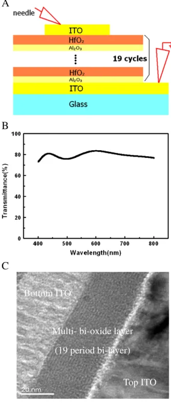
Fig. 1(A) shows the schematic cross-section structure of the de-vice of multi-bi-layer binary transition metal oxide. It reveals the multi-bi-layer binary transition metal oxide made by the 19 periods and each period is composed of HfO2 (12 Å)/Al2O3 (2 Å) bi-layer.
The transmittance of the multi-bi-layer metal oxide is shown in
Fig. 1(B). It is measured by irradiating the ultraviolet–visible light from the top electrode side and receiving at the bottom electrode side ranging from 400 to 800 nm wavelength. High transmittance of about 80% in the average value and 85% in the maximum wavelength can be observed, which reaches nearly fully transparent electronic device. The cross sectional structures of the nanolaminate multi-bi-layer devices were characterized by HR-TEM, as shown inFig. 1(C). Thisfigure clearly demonstrates the multi-bi-layer of the ITO/HfO2/
Al2O3/…/HfO2/Al2O3/ITO capacitor structure with a thickness of
27 nm, which is fairly consistent with the deposition rate. This kind of transparent resistive random access memory [13–15] has drawn attention of widespread applications in consumer devices such as cell phones, computers, TV monitors, and watches.
Before the resistive switching (RS) operation, forming process is needed in the beginning to activate the RS properties. As shown in
Fig. 2 (A), it compares the electroforming current–voltage (I–V) curves of the control and multi-bi-layer-cell sample. A large forming voltage of about−26.4 V was observed on the HfO2sample, while
only about−7.8 V was needed to turn on the multi-bi-layer-cell de-vice. However, if positive bias was used to forming process, the device cannot show predictable or consistent switching characteristics. We speculate that this asymmetric behavior was caused by interface property difference between top and bottom side ITO/TMO (Transi-tion Metal Oxide). The top side ITO was deposited by sputtering. Dur-ing sputterDur-ing process, impDur-ingDur-ing In, Sn or O atom will destroy original well arranged HfO2/Al2O3Bi-layer growth by atomic layer
de-position. The damage interface used as anode during electroforming process can provide many possible filamentary conducting paths resulting irreproducible and unreliable switching characteristics. As negative bias used for forming process, the anode now is at the bot-tom side ITO/TMO interface which has more stablefilamentary con-ducting paths than that of the top interface. The thickness 3–10 nm near the anode plays the important role of the resistive switching property, reported by C. S. Hwang's group[16]. In addition, the leak-age current is significantly different between these two samples. It is below 10 pA for the control device and 10 nA for multi-bi-layer-cell device at−2 V respectively. A multi-bi-layer structure may induce some defects such as oxygen vacancies or interstitials inside the insu-latorfilm, which can contribute on the leakage current by forming conductingfilamentary paths.Fig. 2 (B) and (C) shows the typical unipolar I–V curves of multi-bi-layered stacked sample on linear scale, where positive and negative voltage value was applied to the ITO top electrode, respectively. No switching characteristics can be
observed on HfO2 control samples after electroforming operation,
while the multi-bi-layer stacked sample exhibits the repeated RS characteristics under both bias polarities. We suggest that the RS characteristics may depend on the defect density inside insulator thinfilm. InFig. 2(B) and (C), the voltage sweeps from zero bias to-ward a certain positive or negative bias until the current value in-creased sharply. This bias is defined as Vsetand the state is switched
to low resistance state (LRS). During the next positive bias operation, much larger conducting current mediates through the generated de-fects inside the stacked oxide. The voltage value when the current abruptly decreased is defined as Vreset, and the state is switched to
Bottom ITO
Top ITO
Multi- bi-oxide layer
(19 period bi-layer)
A
B
C
Fig. 1. (A) Schematic cross-section structure of the multi-bi-layer device composed of HfO2/Al2O3/…/HfO2/Al2O3layer, (B) transmittance of the multi-bi-layer device, and (C) cross-sectional TEM image of the multi-bi-layer device.
high resistance state (HRS). Observation on the I–V curves finds that Vsetand Vresetare variable in their voltage value from different
ap-plied polarities, which was influenced by operation polarity. The Vset
and Vresetvalues disperse in the range of 4–7 V and 1–3 V for positive
operation, while concentrate on−0.3 to −1.3 V and −2 to −3.5 V for negative operation. We refer the difference to the asymmetry of the multi-bi-layered stacked structure. The ITO/oxide interface influencing the flow of current, i.e. electron injecting into dielectric film, is easier to pass through ITO/HfO2 interface. This factor
influences not only the switching voltage values but also the resis-tance values on HRS and LRS.
The conducting behaviors of the positive and negative operation I–V curves arefitted, as shown inFig. 3(A)–(C), respectively. The positive switching I–V curve can be well fitted to space-charge-limited current with a slope of 1 in LRS and at the low voltage bias in HRS and a slope of 2 at the high voltage bias in HRS, as shown inFig. 3(A). Oppositely, the negative switching I–V curve was fitted to a different conducting be-havior. An ohmic conduction behavior with a linear slope of 1 was also
Fig. 3. Both HRS and LRS I–V curves can be well fitted to ln (I)–ln (V) curve under pos-itive bias operation. (B) HRS I–V curve under negative bias operation was fitted to ln (I/V)–ln (V) curve. (C) LRS I–V curve under negative bias operation was fitted to ln (I)–ln (V) curve.
Fig. 2. (A) The forming characteristics of the HfO2film and HfO2/Al2O3stacked samples. The I–V curves in continuous resistive switching for 5 times under (B) positive bias, and (C) negative bias on top electrode.
3417 W.-H. Tzeng et al. / Thin Solid Films 520 (2012) 3415–3418
observed in LRS, while changes to Frenkel–Poole emission in HRS. Dif-ferent conducting behaviors may be responsible for difDif-ferent switching characteristics, as shown inFig. 2(B) and (C). We suggest that the ITO/ oxide interface is a critical factor to determine the injected electron to conduction. According to Shiiki et al.[17]and Martinez et al.[18], the bandgap of HfO2and Al2O3thinfilm is about 5.9 and 2.6 eV for
ultra-thinfilm. Difference on the bandgap may modulate the band offset be-tween the oxide and ITOfilm, which dominates the injected electron conduction behavior. For the positive operation, the electron injected from the Al2O3/ITO interface via the defects inside the thin Al2O3
insula-tor. The Al2O3layer is too thin to sustain a good insulatorfilm blocking
the leakage current, thus much injected electrons mediate through the random defects inside the insulatorfilm. Therefore, the electrons con-duct by ohmic concon-duction in the beginning, then followed by the trap-limited and trap-free conduction. For the negative operation, large bandgap of HfO2thinfilm effectively blocks the injected electrons,
thus causing the conducting behavior changes to Frenkel–Poole emis-sion. In addition, the thin defect-riched Al2O3layer can confine the
re-producible formation and rupture of a conducting path at afixed point through the defective structure [19], thus obtaining reliable switching characteristics. Further investigation is needed to elucidate in detail the possible mechanism for the multi-bi-layer stacked struc-ture, leading to better uniformity and reliability of RRAM characteristics. 4. Conclusion
A multi-bi-layer stacked structure based on ITO/HfO2/Al2O3/…/
HfO2/Al2O3/ITO capacitor is fabricated on a glass substrate to form a
transparent resistive random access memory device. The resistive switching characteristics were only observed on the multi-bi-layer stacked structures, which may be attributed to induce more defects or vacancies inside the insulatorfilm. The unipolar resistive switching properties can be demonstrated by both positive and negative
operations. The differences of switching and stability in the two dif-ferent operations may be caused by the difdif-ferent oxide-layer mate-rials toughing the top and bottom electrodes. We refer the difference to the asymmetry of the multi-bi-layered stacked struc-ture, which influences the current flow of the injected electrons. References
[1] I.G. Baek, M.S. Lee, S. Seo, M.J. Lee, D.H. Seo, D.-S. Suh, J.C. Park, S.O. Park, H.S. Kim, I.K. Yoo, U.-In. Chung, J.T. Moon, IEDM Tech. Dig. (2004) 587.
[2] T. Fujii, M. Kawasaki, A. Sawa, H. Akoh, Y. Kawazoe, Y. Tokura, Appl. Phys. Lett. 86 (2005) 012107.
[3] R. Waser, M. Aono, Nat. Mater. 6 (2007) 833.
[4] C. Rohde, B.J. Choi, D.S. Jeong, S. Choi, J.S. Zhao, C.S. Hwang, Appl. Phys. Lett. 86 (2005) 262907.
[5] S. Kim, I. Byun, I. Hwang, J. Kim, J. Choi, B.H. Park, S. Seo, M.J. Lee, D.H. Seo, D.S. Suh, Y.S. Joung, I.K. Yoo, Jpn. J. Appl. Phys. 44 (2005) L345.
[6] K.C. Liu, W.H. Tzeng, K.M. Chang, Y.C. Chan, C.C. Kuo, C.W. Cheng, Microelectron. Reliab. 50 (2010) 670.
[7] N. Das, S. Tsui, Y.Y. Xue, Y.Q. Wang, C.W. Chu, Phys. Rev. B 78 (2008) 235418. [8] J.W. Park, M.K. Yang, K. Jung, J.K. Lee, IEEE Trans. Electron. Dev. 55 (2008) 782. [9] C.Y. Liu, P.H. Wu, A. Wang, W.Y. Jang, J.C. Young, K.Y. Chiu, T.Y. Tseng, IEEE
Elec-tron Dev. Lett. 26 (2005) 351.
[10] S. Seo, M.J. Lee, D.H. Seo, S.K. Choi, D.S. Suh, Y.S. Joung, I.K. Yoo, I.S. Byun, I.R. Hwang, S.H. Kim, B.H. Park, Appl. Phys. Lett. 86 (2005) 093509.
[11] J.H. Choi, S. Nath Das, J.M. Myoung, Appl. Phy. Lett. 95 (2009) 062105. [12] L. Chen, Y. Xu, Q.Q. Sun, H. Liu, J.J. Gu, S.J. Ding, D.W. Zhang, IEEE Electron Dev.
Lett. 31 (2010) 356.
[13] J.W. Seo, J.-W. Park, K.S. Lim, S.J. Kang, Y.H. Hong, J.H. Yang, L. Fang, G.Y. Sung, H.K. Kim, Appl. Phys. Lett. 95 (2009) 133508.
[14] J.W. Seo, J.-W. Park, K.S. Lim, J.H. Yang, S.J. Kang, Appl. Phys. Lett. 93 (2008) 223505.
[15] K.C. Liu, W.H. Tzeng, K.M. Chang, Y.C. Chan, C.C. Kuo, Microelectron. Eng. 88 (7) (2011) 1586.
[16] K.M. Kim, B.J. Choi, C.S. Hwang, Appl. Phys. Lett. 90 (2007) 242906. [17] K. Shiiki, M. Igarashi, H. Kaijyu, Jpn. J. Appl. Phys. 42 (2003) 5185.
[18] F.L. Martinez, M. Toledano-Luque, J.J. Gandia, J. Carabe, W. Bohne, J. Rohrich, E. Strub, I. Martil, J. Phys. D: Appl. Phys. 40 (2007) 5256.
[19] R. Jung, M.J. Lee, S. Seo, D.C. Kim, G.S. Park, K. Kim, S. Ahn, Y. Park, I.K. Yoo, J.S. Kim, B.H. Park, Appl. Phys. Lett. 91 (2007) 022112.