Dielectric properties of Ba
„
Zr
xTi
1Àx…
O
3thin films prepared using radio
frequency magnetron sputtering
Chi-Shiung Hsi
Department of Materials Science and Engineering, I-Shou University, 1 Hsueh-Cheng Road, Section 1, Ta-Hsu, Kaohsiung, 84041, Taiwan
Chung-Yi Chen and Nan-Chung Wu
Department of Materials Science and Engineering, National Cheng Kung University, 1 Ta-Hsueh Road, Tainan, 70101, Taiwan
Moo-Chin Wanga)
Department of Mechanical Engineering, National Kaohsiung University of Applied Sciences, 415 Chien-Kung Road, Kaohsiung, 80782, Taiwan
共Received 15 July 2002; accepted 20 March 2003兲
Pt/Ba(ZrxTi1⫺x)O3/Pt/Ti/SiO2/Si capacitors were fabricated using radio frequency共rf兲 magnetron sputtering. The deposition parameter effects on the dielectric constant, capacitance, and leakage current density of the capacitors were investigated. Amorphous Ba(ZrxTi1⫺x)O3 (BZxT1⫺x) thin films were sputtered onto a substrate with a temperature of 300 °C, rf power of 130 W, and in a no-oxygen atmosphere. BZxT1⫺xthin films deposited onto Pt-coated Si substrates show a preferred orientation in the共100兲 reflection. The dielectric constants of the BZxT1⫺xthin films increased with increasing Zr content and deposition temperature. The diffuse phase transition behavior of the BZxT1⫺xthin films became more pronounced at high Zr content films. The leakage current density of the Pt/Ba(ZrxTi1⫺x)O3/Pt/Ti/SiO2/Si capacitors at 1 kV/cm was about 1.0⫻10⫺7 A/cm2. This increased with increasing deposition temperature but decreased with increasing O2/(O2⫹Ar) ratio. From the films, P – E hysteresis loops, the BZ0.1T0.9thin films had ferroelectric characteristics. The BZ0.3T0.7thin films exhibited paraelectric characteristics at room temperature. © 2003 American Institute of Physics. 关DOI: 10.1063/1.1574179兴
I. INTRODUCTION
Ferroelectric thin film materials with ABO3 perovskite-type structure have attracted much attention for memory ap-plications. In dynamic random access memory 共DRAM兲 ap-plication, polarization hysteresis behavior is not required.1In an 1 G Bit DRAM, the memory arrays contain 109 cells sur-rounded by peripheral devices that manage the command and voltage levels.2All DRAM chips manufactured to date use capacitors containing electrodes made of doped silicon or polysilicon and dielectric silicon dioxide and/or silicon ni-tride film. Incorporating a new dielectric film into the capaci-tor will break a 30 years precedent where long term dielectric performance and reliability are firmly established.2
The following three features have crucial importance for the quality and reliability of memory devices: fast dielectric response, low leakage current loss and long lifetime. Re-cently, high dielectric constant ferroelectric thin film materi-als such as BaTiO3,
3–5
Pb(Zr,Ti)O3, 6
(Ba,Pb)(Zr,Ti)O3, 1,7 and (Ba,Sr)TiO3 共Refs. 8–14兲 have generated great interest for cell capacitor applications in DRAMs that require very high storage charge densities. Among these materials, ferro-electric barium strontium titanite关(Ba,Sr)TiO3,BST兴 film is one of the most promising capacitor materials for future DRAM applications because of its high dielectric constant and low leakage current at operating voltages.12,13
The BST ceramic is a solid solution of BaTiO3共BT兲 and SrTiO3 共ST兲, and can be expressed as x BT– (1⫺x)ST. Zir-conia (ZrO2) was shown by Brager15 and Kulscar16 to in-crease the orthorhombic–tetragonal transition temperature of BT while slightly lowering the tetragonal–cubic transition temperature. Addition of unstabilized ZrO2 to BaTiO3 re-tards the grain growth and decreases the Curie temperature accompanied with a reduced c/a ratio and a decrease in the spontaneous polarization.17 A flat permittivity profile be-tween 30 and 125 °C with significantly lower dielectric loss has also been measured from unstabilized ZrO2 doped BaTiO3.17
Ferroelectric Pb(Zr,Ti)O3 thin films possessing a broad range of chemical compositions have been applied in pyro-electric, piezopyro-electric, and electro-optic devices.18 Hu and Krupanidhi6pointed out that the degree of共100兲 orientation, remnant polarization, coercive field, and dielectric constant of ferroelectric Pb(Zr,Ti)O3 thin films are strongly depdent on the ion-beam flux and oxygion bombardment en-ergy. Barium lead zirconate titanate关(Ba,Pb)(Zr,Ti)O3兴 thin films have been successfully fabricated from a stoichiometric target using rf magnetron sputtering. The dielectric proper-ties of these films were investigated by Torii et al.7However, studies on Ba(ZrxTi1⫺x)O3 (BZxT1⫺x) thin film deposition using rf magnetron sputtering and their dielectric properties have not been conducted.
a兲Electronic mail: mcwang@cc.kuas.edu.tw
598
cess. The structures and dielectric properties of these films were investigated, using x-ray diffraction 共XRD兲, scanning electron microscopy 共SEM兲, and capacitance–voltage and current–voltage measurements. The influences of the pro-cessing parameters on the crystal structures, microstructures, and dielectric properties of BZxT1⫺xthin films are discussed.
II. EXPERIMENTAL PROCEDURE A. Thin film deposition
Stoichiometric Ba(ZrxTi1⫺x)O3 ceramic targets with various Zr contents were prepared. The chemical composi-tions of these targets are listed in Table I. Commercial BaZrO3 共purity 99.0%, supplied by Johnson Matthey, Inc., West Chester, PA兲 and BaTiO3 共purity 99.0%, supplied by Noah Tech. Co., San Antonio, Texas兲 were weighted and ball milled with acetone and alumina balls for 10 h. The mixed slurries were dried using an infrared lamp and subsequently ground and passed through an 80 mesh sieve. The powders were then mixed with a 1.0 wt % polyvinyl acetate 共PVA兲 binder and pressed into 5.0-cm-diam disks at 180 MPa pres-sure. The pressed disks were heat treated at 600 °C for 30 min with a 4.5 °C/min heating rate to burn out the binder. The binder burned out target disks were then heated at 1100 °C for 2 h with a 1.5 °C/min heating rate, and cooled to room temperature at a rate of 3 °C/min.
The n-type Si共100兲 wafer substrates were cleaned using a standard process. The substrate dimensions were 10.0 mm width, 10.0 mm length, and 0.50 mm thickness. A 200.0 nm silicon oxide layer was grown on top of the silicon substrate using thermal oxidation. Platinum 共Pt兲 layers were used as the top and bottom electrodes in the capacitors structure. The 500.0-nm-thin Pt bottom electrode was sputter deposited on the top of 5.0 nm Ti film at a temperature of 400 °C. Both metals were sputtered in an Ar atmosphere at a working pres-sure of 1.0⫻1.0⫺2Torr with an applied power of 150 W.
Ba(ZrxTi1⫺x)O3 (BZxT1⫺x) thin films with various Zr contents were deposited on Pt films using rf magnetron sput-tering. The parameters for the BZxT1⫺x thin film deposition processes are listed in Table II. The thickness of the dielec-tric films was 500 nm. The Pt top electrodes were patterned using a shadow mask process with a thickness of 50.0 nm and diameters of 150.0, 250.0, and 350.0 nm, respectively.
B. Properties characterization
The thickness of the BZxT1⫺x thin films with various ZrO2contents was measured using an automatic ellipsometer
共Rudolph Research Co., Flanders, NJ兲 with a He–Ne laser 共wavelength 6328 Å兲 as a detecting probe and a profilometer 共Tencor Alpha-Step 200, San Jose, CA兲.
BZxT1⫺x thin film cross section microstructures were observed using SEM共Hitachi, model S-4200, Tokyo, Japan兲. The BZxT1⫺x thin film crystal structures were analyzed us-ing XRD共Rigaku Co., model Rad IIA, Tokyo, Japan兲, using Cu K␣ radiation.
The dielectric constants of the BZxT1⫺xfilms were mea-sured at temperature from 20 to 160 °C using an impedance analyzer 共HP 4192 A LF, Palo Alto, CA兲 with a thermostat 共Mini-subzero MC-81, Kisnet, Japan兲 using an applied ac voltage of 1 V and a frequency of 1 kHz. The dielectric constant (r) was calculated using Eq.共1兲:
r⫽
Cd
0A
, 共1兲
where C is the capacitance共F兲, d is the film’s thickness 共m兲, A is the area of Pt top electrode共m2兲, and 0 is the permit-tivity of the free space (8.854⫻10⫺12F/m).
The capacitance–bias voltage curves in the range from ⫹5 to ⫺5 V with a stair step voltage of 0.2 V were measured at 100 kHz and 25 °C using an impedance analyzer. The current–voltage sweep of the Pt/BZxT1⫺x/Pt/Ti/SiO2/Si ca-pacitors from 0 to 40 V was measured with an HP 4156 B semiconductor parameter analyzer at 0.2 V dc stair step volt-age, 5 s holding time, 20 s delay time, and 25 °C measure-ment temperature. A 1 nF mica capacitor was used to detect the amount of stored charge.
III. RESULTS AND DISCUSSION
A. Crystal structure and microstructure of the BZxT1Àx thin film
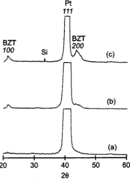
The XRD profiles of the BZ0.3T0.7thin films sputtered at 130 W rf power; 5.0⫻10⫺3Torr working pressure; O2/(O2 ⫹Ar) ratio of 1/10; and 300, 400, and 500 °C substrate tem-peratures, are shown in Fig. 1. BZ0.3T0.7phases in the (h00) reflections and Pt 共111兲 reflection were observed. The pre-ferred orientation of BZ0.3T0.7 in the (h00) reflections indi-cated that the BZ0.3T0.7 thin film consisted of a single BaZrxTi1⫺xO3 phase epitaxially grown onto the substrate. The crystallinity of the BZ0.3T0.7 phase increased with creasing substrate temperature. This was caused by an in-crease in kinetic energy in the sputter-ejected species with increasing substrate temperature, leading to enhanced BZ0.3T0.7thin film crystalization.19
An amorphous BZ0.3T0.7thin film was obtained when the film was prepared at 130 W rf power, 5.0⫻10⫺3 Torr work-ing pressure, 300 °C substrate temperature, and an O2/(O2 ⫹Ar) ratio of 0, as shown in Fig. 2共a兲. The crystallinity of the BZ0.3T0.7 thin films increased with increasing O2/(O2 ⫹Ar) ratio, as indicated by curves 共b兲 and 共c兲 in Fig. 2. The oxygen partial pressure played a crucial role in the film’s growth process.20Oxygen addition to the sputtering gas, en-hancing indium tin oxide film crystallization, was reported by Buchanan et al.21
The SEM micropraph of the BZ0.3T0.7/Pt/Ti/SiO2/Si structure prepared at 130 W rf power, 5.0⫻10⫺3 Torr work-ing pressure, 500 °C substrate temperature, and an O2/(O2
⫹Ar) ratio of 1/10 is shown in Fig. 3. A dense and crack-free BZ0.3T0.7film was fabricated on the top of the substrate. The film thickness was 500 nm and columnar grains were ob-served from the BZ0.3T0.7film cross section.
B. Dielectric constant of the BZxT1Àx thin film
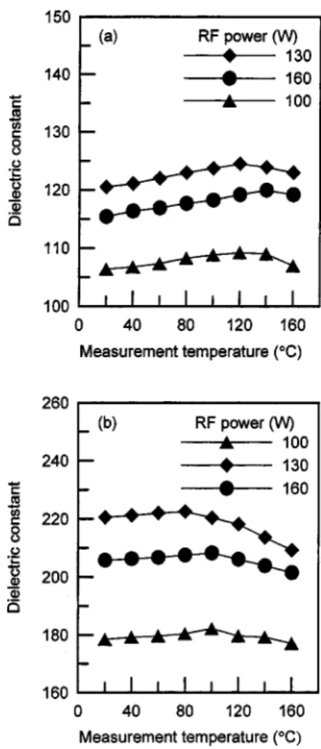
Figures 4 – 6 show the dielectric constants of the BZxT1⫺x thin films (x⫽0.1– 0.3) at different measurement temperatures. When BZ0.1T0.9 thin films were deposited at 100 W rf power with a substrate temperature of 300 °C, the maximum dielectric constant was obtained at 120 °C, as shown in Fig. 4共a兲. The Curie temperature was close to the Curie temperature of the BT structure because it had only 10 mol % Zr in the BZxT1⫺x film. When the BZ0.1T0.9thin film was deposited at 160 W rf power and a substrate temperature of 300 °C, variations in the film dielectric constant at the Curie temperature, 120 °C, were not quite pronounced. The Curie temperature of the BZxT1⫺x thin films became less obvious when the films had a ZrO2 content greater than 20 mol %, as shown in Figs. 5共a兲 and 6共a兲. This indicated that BZ0.3T0.7thin films sputtered at 100 W rf power and a sub-strate temperature of 300 °C were amorphous.19 Diffuse phase transition behaviors were observed with increasing Zr content in BZxT1⫺x thin films.
The dielectric constants of BZxT1⫺xthin films deposited at 300 and 500 °C increased with increasing deposition tem-perature and Zr content, as revealed in Figs. 4– 6. The maxi-mum dielectric constants of the BZxT1⫺x thin films were obtained from samples prepared using 130 W rf power. Resputtering,19,22 lead to decreased crystallinity of the BZxT1⫺x thin films with the rf power increasing from 130 to 160 W, which might cause a decrease in the film dielectric constant. The dielectric constant of the BZxT1⫺x thin films increased with increasing Zr content at the same deposition rf power.
Figure 7 shows the relationships between the frequency and capacitance of Pt/BZ0.3T0.7/Pt/Ti/SiO2/Si capacitors de-posited at different substrate temperatures. The capacitance decreased with increasing frequency. Each sample’s capaci-FIG. 1. XRD patterns of BZ0.3T0.7thin films sputtered at various substrate
temperatures:共a兲 300 °C, 共b兲 400 °C, and 共c兲 500 °C. The deposition condi-tions were 130 W rf power, 5.0⫻10⫺3Torr working pressure, and an O2/(O2⫹Ar) ratio of 1/10.
FIG. 2. XRD patterns of BZ0.3T0.7thin films deposited at various O2/(O2
⫹Ar) ratios: 共a兲 0, 共b兲 1/10, and 共c兲 2/10. The deposition conditions were
130 W rf power, 5.0⫻10⫺3Torr working pressure, and 300 °C substrate temperature.
FIG. 3. SEM micrograph of Pt/BZ0.3T0.7/Pt/Ti/SiO2/Si sputtered at 130 W
rf power, 5.0⫻10⫺3Torr work pressure, an O2/(O2⫹Ar) ratio of 1/10, and
tance decreased at the measuring frequencies from 1 k to 40 kHz. The capacitance of the films reached equilibrium values when the frequency was greater than 40 kHz. Each curve had a depression at various frequencies caused by capacitor reso-nance leading to decreased dielectric constant. The capaci-tance decreased with decreasing substrate temperature when measured at the same frequency. As revealed from Fig. 1, a better BZxT1⫺x phase crystallinity was observed from samples deposited at higher substrate temperatures. This caused the film capacitance to be higher.
The capacitances of Pt/BZ0.3T0.7/Pt/Ti/SiO2/Si capaci-tiors deposited at 130 W rf power, 5.0⫻10⫺3 Torr working pressure, and an O2/(O2⫹Ar) ratio of 1/10 at different bias voltages are shown in Fig. 8. The electric charge storage of BZ0.3T0.7 thin films deposited at 300 °C had consistent ca-pacitance values at different bias voltages. This indicated the films linear dielectric behavior. In Waser’s investigation,23 superparaelectric behavior was obtained from ferroelectric BT thin films due to their small grain size. The grain sizes of the BZxT1⫺x thin films were inhibited by the addition of Zr.24 In this study, a broadened BZ0.3T0.7 phase peak oc-curred in the共100兲 reflection of the XRD profile of thin films deposited at 300 °C. This revealed the small grain size of the
films, as shown in curve 共a兲 in Fig. 1. The linear dielectric characteristics of the BZ0.3T0.7 thin films were due to the small grain size. Variations of the capacitances of BZ0.3T0.7 thin films deposited at 400 and 500 °C at 4 V bias voltage were greater than 20 pF. The electric charge storage of those films decreased with increasing bias voltage. Nonlinear di-electric properties were observed from 400 and 500 °C de-posited BZ0.3T0.7 thin films. As discussed previously, the crystallinity and grain size of BZ0.3T0.7 thin films increased with increasing substrate temperature from 300 to 500 °C. Due to the larger grain size, BZ0.3T0.7 thin films deposited onto 400 and 500 °C substrates exhibited nonlinear dielectric behavior.
C. Leakage current density of the PtÕBZxT1ÀxÕPtÕTiÕSiO2ÕSi capacitors
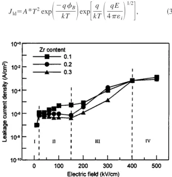
The influences of the electric field and Zr content on the leakage current density of the Pt/BZxT1⫺x/Pt/Ti/SiO2/Si ca-pacitors are shown in Fig. 9. The leakage current density of the Pt/BZxT1⫺x/Pt/Ti/SiO2/Si capacitors at 1 kV/cm is about 1.0⫻10⫺7 A/cm2 (x⫽0.1– 0.3). The leakage current densities of the BZ0.3T0.7 capacitors were lower than other BZxT1⫺xcapacitors. Similar electric field versus leakage cur-FIG. 4. Dielectric constants of共a兲 300 °C and 共b兲 500 °C deposited BZ0.1T0.9
thin films as a function of the measured temperatures. Deposition conditions of these films were 100, 130, and 160 W rf power; 5.0⫻10⫺3Torr working pressure; and an O2/(O2⫹Ar) ratio of 1/10.
FIG. 5. Dielectric constants of共a兲 300 °C and 共b兲 500 °C deposited BZ0.2T0.8
thin films as a function of the measured temperatures. Deposition conditions of these films were 100, 130, and 160 W rf power, 5.0⫻10⫺3Torr working pressure, and an O2/(O2⫹Ar) ratio of 1/10.
rent density characteristics were observed from different Zr content capacitors at applied electric fields between 150 and 400 kV/cm. BZ0.3T0.7 thin films
19
had a higher crystallinity. This gave the films the lowest leakage current density among
the films prepared in this study. The leakage current (Ilc) of the Pt/BZxT1⫺x/Pt/Ti/SiO2/Si capacitors can be expressed as:12
Ilc⫽Ise⫹It⫹Idt⫹Ith, 共2兲 where Iseis the current flow using the Schottky emission, It
is the tripping current, Idtis the detripping current, and Ithis the thermally generated current.
The Schottky-barrier limited current flow was reported as the most favored mechanism for the leakage current in ST and (Ba,Sr)TiO3thin films.11,13,25,26The height of the barrier is in the general field and temperature dependent. The Schottky effect quantifies the field effect on the energy bar-rier for the electron emission from a metal into a semicon-ducting or insulating bulk materials.27 The temperature de-pendence 共T兲 and electric field 共E兲 on the leakage current density (Jld) can be expressed as28
Jld⫽A*T2exp
冉
⫺qB kT冊
exp冋
q kT冉
qE 4i冊
1/2册
, 共3兲FIG. 6. Dielectric constants of共a兲 300 °C and 共b兲 500 °C deposited BZ0.3T0.7
thin films as a function of the measured temperatures. Deposition conditions of these films were 100, 130, and 160 W rf power, 5.0⫻10⫺3Torr working pressure, and an O2/(O2⫹Ar) ratio of 1/10.
FIG. 7. Capacitance vs frequency of Pt/BZ0.3T0.7/Pt/Ti/SiO2/Si capacitors
sputtered at 130 W rf power, 5.0⫻10⫺3Torr working pressure, and an O2/(O2⫹Ar) ratio of 1/10.
FIG. 8. Bias voltage vs capacitance of the Pt/BZ0.3T0.7/Pt/Ti/SiO2/Si
ca-pacitors sputtered at 130 W rf power, 5.0⫻10⫺3Torr working pressure, and an O2/(O2⫹Ar) ratio of 1/10.
FIG. 9. Leakage current densities of the Pt/BZxT1⫺x/Pt/Ti/SiO2/Si
capaci-tors at different applied electric fields. Dielectric layers of the capacicapaci-tors were prepared at 130 W rf power, 5.0⫻10⫺3Torr working pressure, an O2/(O2⫹Ar) ratio of 1/10, and 500 °C substrate temperature.
where A* is the effective Richardson constant, T is the ab-solute temperature, q is the electron charge,B is the barrier height, E is the electric field, i is the insulator dynamic dielectric constant, and k is the Boltzmann constant.
In this case, the charge carriers were thermally excited over an energy barrier at the ceramic–metal interface. This barrier was created using the equilibration of the charge car-rier energy in the ceramic and metal. The equilibration value at zero applied field was adjusted by field-dependent lower-ing of the barrier resultlower-ing from image forces.11
In Fig. 9, the electric field effect on the leakage current density was divided into four regimes. Electric fields smaller than 20 kV/cm were located in regime I共Ohmic regime兲. At this regime, the thermally generated currents in both direc-tions were only slightly affected by the external field. The electric fields from 20 to 150 kV/cm belonged to regime II, where the voltage-independent forward current led to a satu-ration current. Regime III had electrical fields from 150 to 400 kV/cm. In this regime the barrier became lower due to the Schottky emission effect. Electric fields larger than 400 kV/cm were attributed to regime IV. Murphy and Good26 pointed out that neither the Schotthy emission nor the Fowler–Nordheim tunneling approximation works in this regime.29
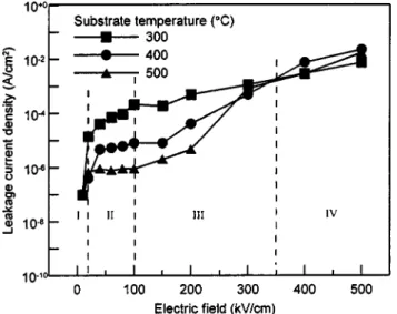
The electric field and substrate temperature effects on the leakage current density of the Pt/BZ0.3T0.7/Pt/Ti/SiO2/Si capacitors are shown in Fig. 10. The leakage current densi-ties of the capacitors increased with increasing substrate tem-peratures. This result was caused by Ti4⫹ reduced to Ti3⫹, and the oxygen vacancies generated at elevated substrate temperatures. The oxygen vacancies act as doubly ionized donors and contribute, at maximum, two electrons to the electrical conductivity as shown in the following equation:20
OO2⫺→VO""⫹2e
⬘
⫹12O2共g兲. 共4兲 The interface between the Pt electrode and the BZ0.3T0.7 thin film was also associated with the field-enhanced thermal
excitation charge carriers from the traps due to the increasing substrate temperature.4These thermal excitation charge car-riers made the capacitor leakage current densities increase with increasing sputtering temperature.
Figure 11 shows the effects of the electric field and O2/(O2⫹Ar) ratio on the leakage current densities of the Pt/BZ0.3T0.7/Pt/Ti/SiO2/Si capacitors. The leakage current densities decreased with increasing O2/(O2⫹Ar) ratio. This was caused by oxygen vacancy dissipation, leading to a de-crease in resistivity. Ovadyahu et al.28 found dendritic growth in indium oxide films when the partial oxygen pres-sure was lower than the nominal prespres-sure. The indium oxide films with dendritic structures had poor electrical properties. Thilakan and Kumar30reported that a few oxygen vacancies acted as charge carriers in films at high oxygen partial pres-sure. The critical role of oxygen partial pressure on sputter-ing gas is the conflictsputter-ing requirements for introducsputter-ing enough oxygen vacancies without creating too many grain boundaries in the process.20
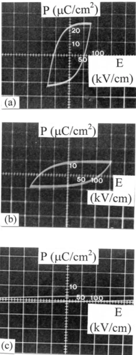
Figure 12 shows the polarization versus electric field ( P – E) hysteresis loops in BZxT1⫺xthin films. The BZxT1⫺x thin film with x⫽0.1 共10 mol % of Zr兲 exhibited a square hysteresis loop and remnant polarization ( Pr) of 21C/cm2. When the film had 20 mol % Zr, the remanent polarization of the BZ0.2T0.8 thin film decreased to 10 C/cm2. The P – E characteristics of BZ0.3T0.7 thin films exhibited linear rela-tionships. These films had a paraelectric behavior. The paraelectric characteristics of the BZ0.3T0.7 thin films were consistent with previous discussions on temperature and bias field dependences of dielectric constants.
IV. CONCLUSIONS
BZxT1⫺x thin films with various Zr contents were suc-cessfully fabricated from stoichiometric targets using rf mag-netron sputtering. BZxT1⫺xthin films deposited on Pt-coated Si substrates had preferred orientation in the共100兲 reflection. The Curie temperatures of the BZxT1⫺x thin films were not FIG. 10. Leakage current densities of the Pt/BZ0.3T0.7/Pt/Ti/SiO2/Si
capaci-tors at different applied electric fields. Dielectric layers of the capacicapaci-tors were prepared at 130 W rf power, 5.0⫻10⫺3Torr working pressure, and an O2/(O2⫹Ar) ratio of 1/10.
FIG. 11. Leakage current densities of the Pt/BZ0.3T0.7/Pt/Ti/SiO2/Si
capaci-tors at different applied electric fields. The dielectric layers of the capacicapaci-tors were prepared at 130 W rf power, 5.0⫻10⫺3Torr working pressure, and 500 °C substrate temperature.
pronounced when the Zr content of the films increased. Dif-fuse phase transformation was observed in the prepared films. Due to the better BZxT1⫺x phase crystallinity formed in the film, the dielectric constant of the BZxT1⫺x thin films increased with increasing deposition temperatures and Zr content. Linear dielectric behaviors were obtained from BZ0.3T0.7thin films deposited onto 300 °C Pt-coated Si sub-strates. When the substrate temperatures increased, the di-electric of the BZ0.3T0.7 thin films became nonlinear. The leakage current density at 1 kV/cm was about 1.0 ⫻10⫺7 A/cm2for 0.1⭐⫻⭐0.3. The leakage current density increased with increasing substrate temperature but
de-creased with increasing O2/(O2⫹Ar) ratio. The hysteresis loops in the polarization versus electric field plots indicated that the BZ0.3T0.7 thin films had paraelectric properties at room temperature.
ACKNOWLEDGMENTS
This work was supported by the National Science Coun-cil, Taiwan, Republic of China under Contract No. NSC89-2216-E-151-004, which is gratefully acknowledged. Help in experimental work and suggestions were received from Pro-fessor M. P. Hung, ProPro-fessor M. H. Hon, Mr. S. Y. Yao, and Mr. J. M. Chen. Their participation is deeply appreciated.
1K. Torii, Ferroelectrics 152, 157共1994兲. 2D. E. Totecki, Integr. Ferroelectr. 16, 1共1997兲.
3B. S. Kwak, K. Zhang, E. P. Boyd, A. Erbil, and B. J. Wilkens, J. Appl.
Phys. 69, 767共1991兲.
4
P. Li and T. M. Lu, Phys. Rev. 43, 14261共1991兲.
5K. Iijima, T. Terashima, K. Yamamoto, K. Hirata, and Y. Bando, Appl.
Phys. Lett. 56, 527共1990兲.
6H. Hu and S. B. Krupanidhi, Appl. Phys. Lett. 61, 1246共1992兲. 7
K. Torri, T. Kaga, and E. Takeda, Jpn. J. Appl. Phys., Part 1 31, 2989 共1992兲.
8T. Tsurumi, T. Miyasou, Y. Ishibashi, and N. Ohashi, Jpn. J. Appl. Phys.,
Part 1 37, 5104共1998兲.
9Y. Fukuda, H. Haneda, I. Sakaguchi, K. Numata, A. Aoki, and A.
Nish-imura, Jpn. J. Appl. Phys., Part 2 36, L1514共1997兲.
10B. A. Baumert, L. H. Chang, A. T. Matsuda, T. L. Tsai, C. J. Tracy, R. B.
Gregoy, P. L. Fejes, N. G. Cave, W. Chen, D. J. Taylor, T. Otsuki, E. Fujii, S. Hayashi, and K. Suu, J. Appl. Phys. 82, 2558共1997兲.
11
G. W. Dietz, M. Schumacher, R. Waser, S. K. Streiffer, C. Basceri, and A. I. Kingon, J. Appl. Phys. 82, 2359共1997兲.
12J. H. Joo, Y. C. Jeon, J. M. Seon, K. Y. Oh, J. S. Roh, and J. J. Kim, Jpn.
J. Appl. Phys., Part 1 36, 4382共1997兲.
13Y. P. Wang and T. Y. Tseng, J. Appl. Phys. 81, 6762共1997兲. 14
T. Horikawa, N. Mikami, T. Makita, J. Tanimura, M. Kataoka, K. Sato, and M. Nunoshita, Jpn. J. Appl. Phys., Part 1 32, 4126共1993兲.
15E. J. Brajer, U.S. Patent No. 2708243共1955兲. 16F. Kulscar, U.S. Patent No. 2735024共1956兲. 17
T. R. Armstrong, L. E. Morgens, A. K. Maurice, and R. C. Buchanan, J. Am. Ceram. Soc. 72, 605共1989兲.
18L. M. Sheppard, Ceram. Bull. 71, 85共1992兲.
19M. C. Wang, C. Y. Chen, C. S. Hsi, and N. C. Wu, J. Cryst. Growth 246,
99共2002兲.
20
R. B. H. Tahar, T. Ban, Y. Ohya, and Y. Takahashi, J. Appl. Phys. 83, 2631 共1998兲.
21M. Buchanan, J. B. Webb, and D. F. Williams, Appl. Phys. Lett. 37, 213
共1980兲.
22D. J. Kester and R. Messier, J. Mater. Res. 8, 1928共1993兲. 23
R. Waser, in Science and Technology of Electroceramic Thin Films, edited by O. Auciello and R. Waser共Kluwer Academic, Dordrecht, The Nether-lands, 1995兲, pp. 223–248.
24D. W. Hoffman and R. Waser, Integr. Ferroelectr. 17, 141共1997兲. 25
R. Waser, Ferroelectrics 15, 39共1991兲.
26
E. L. Murphy and R. H. Good, Phys. Rev. 102, 1464共1956兲.
27G. W. Dietz, W. Antpo¨hler, M. Klee, and R. Waser, J. Appl. Phys. 78, 6113
共1995兲.
28Z. Ovadyahu, B. Ovryn, and H. W. Kraner, J. Electrochem. Soc. 130, 917
共1983兲.
29J. F. Scott, Integr. Ferroelectr. 9, 1共1995兲.
30P. Thilakan and J. Kumar, Thin Solid Films 292, 50共1997兲.
FIG. 12. Polarization vs electric field ( P – E) curves of the BZxT1⫺x thin films:共a兲 x⫽0.1, 共b兲 x⫽0.2, and 共c兲 x⫽0.3.